
 Open Access Article
 This Open Access Article is licensed under a Creative Commons Attribution-Non Commercial 3.0 Unported Licence
Highly conductive flat grains of cesium lead bromide perovskites via additive engineering with methylammonium bromide†
Chandra Shakher
Pathak
 *ab,
Deepak
Aloysius
c,
Satyajit
Gupta
*c,
Sabyasachi
Mukhopadhyay
d and
Eran
Edri
a
*ab,
Deepak
Aloysius
c,
Satyajit
Gupta
*c,
Sabyasachi
Mukhopadhyay
d and
Eran
Edri
a
aDepartment of Chemical Engineering, Ben-Gurion University of the Negev Beer Sheva, 8410501, Israel. E-mail: cspathak12@gmail.com
bDepartment of Physics, BMS Institute of Technology and Management, Avalahalli, Bengaluru, 560064, India
cDepartment of Chemistry, Indian Institute of Technology Bhilai, Chhattisgarh, 492015, India. E-mail: satyajit@iitbhilai.ac.in
dDepartment of Physics, SRM University – AP, Andhra Pradesh 522240, India
First published on 26th August 2024
Abstract
Perovskite solar cells made of inorganic cesium lead bromide (CsPbBr3) display unusually high open-circuit potentials. Yet, their photovoltaic efficiency is still lagging behind that of iodide-based halide perovskites. In this study, a multistep solution spin coating process is used to create a CsPbBr3 film. The CsPbBr3 perovskite film consists of flat and rounded grains, and the photocurrent of each grain type is imbalanced. Interestingly, a significant current increase in flat grains is observed when conducting atomic force microscopy (c-AFM) at the nanoscale after the addition of methyl ammonium bromide (MABr) as an additive. The addition of MABr results in good optoelectronic quality of perovskite films with highly conductive grains and enables better charge transport and hence improved power conversion efficiency.
Introduction
Organic–inorganic hybrid perovskite solar cells (PSCs) have made significant advancements in recent years, demonstrating steady growth in their development.1–4 The main factors that help to improve the performance of PSCs are the composition, interface engineering, and light-harvesting characteristics of the perovskite material.5–9 Perovskite thin films typically exhibit microstructures characterized by grains and grain boundaries (GBs). The engineering of these films, along with microscopic research, is essential for advancing PSCs.It has also been demonstrated that surface and GB modifier additives can enhance the PSC performance by affecting the morphology and ‘surface trap’ passivation. Small molecules10–15 and potassium halide layers16,17 were adsorbed at the GBs and surfaces to passivate surface defects, reduce non-radiative losses, increase carrier lifetimes, and enhance the open-circuit voltage (Voc). Polymers were incorporated into the precursor solutions to passivate defects, thereby enhancing the performance and extending the lifetime of PSCs.18–24
Perovskite solar cells made of inorganic cesium lead bromide (CsPbBr3) have displayed unusually high open-circuit potentials. Their photovoltaic efficiency, however, continues to be inferior to that of iodide-based halide perovskites. To improve the performance of CsPbBr3 PSCs, a range of additives and interface materials have been employed.25–33 Huang et al.34 used cesium acetate (CsAc) and the ionic liquid methylammonium acetate (MAAc) to suppress the defects and to prepare a uniform, high-coverage CsPbBr3 film with larger crystalline grains. The improved power conversion efficiency (PCE) of the additive is attributable to the favorable morphology, decreased non-radiative recombination, and increased interfacial charge transfer. Furthermore, grains or GBs are crucial to the performance and long-term stability of PSCs. In the case of CsPbBr3, flat grains were normally observed28,35–41 but the electronic properties of these flat grains have not been investigated in detail, and studies on their impact on device performance are currently lacking. Recently we performed the comparison between CsPbBr3 and MAPbBr3 perovskites and showed that the former perovskite has higher thermal stability.42 High-resolution studies utilizing electrical modes of scanning probe microscopy (SPM) techniques, such as conductive atomic force microscopy (c-AFM) and Kelvin probe force microscopy (KPFM), can effectively investigate the crucial role of grains and GBs in influencing the performance and stability of PSCs.7,43–51 Previously, a factor of 10 increase in current caused by thermal aging in the absorbing CsPbBr3 halide perovskite layer was measured using c-AFM.35
Using KPFM, one can image the contact potential difference of a material and gain important information on the grains and GBs.7,43–47,52–55 KPFM can also be employed to demonstrate the shift in the Fermi level of CsPbBr3 with BiBr3 as an additive, which facilitates the efficient separation and transport of photogenerated charge carriers, thereby enhancing device performance.56
In this study, we used c-AFM and KPFM to investigate the optoelectronic properties of flat grains with the addition of methylammonium bromide (MABr) to cesium bromide (CsBr) solution as an additive for CsPbBr3-PSCs. By doping MABr in a CsBr/methanol solution, a high-quality CsPbBr3 perovskite absorber layer is produced, which has a better crystalline quality and a higher photocurrent. The addition of MABr makes the CsPbBr3 grains more conductive, especially the flat grains than the bare ones, and a highly significant increase in overall current is observed. We also observed a higher surface potential for flat grains by KPFM measurements, and the optoelectronic quality was greatly improved. The overall increase in current was further confirmed by macroscopic measurements of PSCs. We successfully fabricate high optoelectronic quality CsPbBr3 grains and thus perovskite films prepared with optimized MABr content having improved morphology, light absorbance, and suitable energy levels for efficient charge transport.
Experimental section
Materials
Lead bromide (PbBr2, 98+%, extra pure) was purchased from Acros Organics. Cesium bromide (CsBr, 99.9%, metal basis) and bis(trifluoromethane)sulfonamide lithium salt (LiTFSI, 98.0+%) were purchased from Alfa Aesar. Titanium tetrachloride (TiCl4, 99.0%) solution was purchased from Sigma-Aldrich, and titanium dioxide (30NR-D TiO2) paste was purchased from Greatcell Solar Materials. Dimethyl formamide (DMF, 99.0%), acetonitrile (99.5+%), and chlorobenzene (99.9%) were used as purchased from Alfa Aesar. Dimethyl sulfoxide (DMSO, 99.8%) was purchased from Acros Organics. Ethanol absolute (dehydrated, AR CAS 64-17-5), hydrochloric acid (AR 32%; CAS 7464-01-0), and methanol were purchased from Bio-Lab Ltd, Jerusalem, Israel. Isopropanol and 4-tert-butylpyridine (tBP, 96.0%) were purchased from Sigma-Aldrich. PTAA (batch no. 20210512) was purchased from Broun New Material Technology Ltd.Fabrication of films and PSCs
Alconox detergent powder, deionized (DI) water, acetone, and 2-propanol were used to clean fluorine-doped tin oxide (FTO) substrates for 30 minutes each, followed by 30 minutes of UV-ozone treatment.The J–V curves of the PSCs were obtained under simulated AM 1.5G (100 mW cm−2) illumination, produced by a ScienceTech AAA solar simulator, and measured using an Ossila Source-Measure Unit. The light intensity was calibrated to 100 mW cm−2 using a standard silicon reference cell certified by the Newport Corporation.
Results and discussion
c-AFM experiments of the glass/FTO/c-TiO2/m-TiO2/perovskite with and without MABr were carried out to examine the impact of MABr incorporation on the morphology and electrical characteristics at the nanoscale. The topography and related current map of perovskite films with MABr under illumination are shown in Fig. 1. The topography image of the perovskite films shows that the grains have flat and rounded layered surfaces, and this type of structure is normally observed,28,35–41,57 but the investigation of this type of grain has not been conducted previously. To gain insight into the conduction behavior of the flat grains, nanoscale photocurrents were mapped using c-AFM. The current is not uniformly distributed throughout the surface for the bare film, preferentially flowing through the flat grain sides; however, with increasing MABr content, the current is more uniform, and GBs also show higher currents, as shown in Fig. 1. We found the average current for the overall area to be 1.18 pA for bare and 100.4 pA for 15 mg MABr films at 0 V, which indicates that the current was significantly enhanced. Bias application further enhanced the effective separation of photogenerated charge carriers and increased the photocurrents. The addition of MABr significantly improved the overall homogeneity of the current signal, which denotes a stronger electrical conductivity of the film and, thus, improved charge transfer. This shows that the surface trap states were effectively passivated by the MABr. It is worth noting that the GBs exhibit a comparatively larger current flow, which is consistent with more effective charge transfer. For the bare film, the grains are inefficient for charge transfer, which results in poor conductivity of the film. Charge transport across the GBs is made more effective by MABr passivation, which lowers the number of non-radiative recombination sites. Accordingly, MABr can enhance the crystallinity of the perovskite layer and reduce defects at GBs, which facilitates the charge transfer.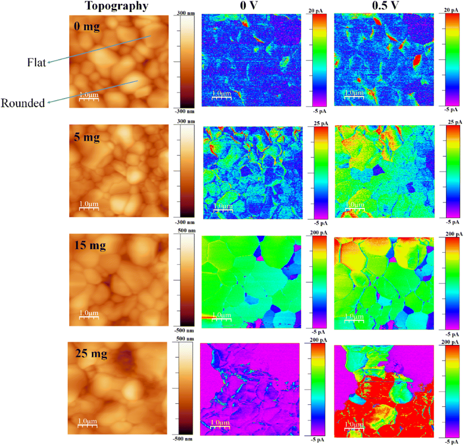 | ||
| Fig. 1 Topography and the corresponding current maps of perovskite films with MABr under illumination. | ||
A very low current signal was seen in the flat grains of the bare perovskite, indicating poor mobility and/or depleted charge carriers in the flat region.58
The current line profile in Fig. S1 (ESI†) shows that the flat grain exhibits a lower current than the rounded grain for the bare perovskite. However, after the addition of MABr, the flat grains display a higher current than the bare perovskite and approach the current value of the rounded grains.
A lower current of flat grains compared to rounded grains was also observed previously.35 According to the literature, different crystallographic orientations may cause different photoresponses.59 Here, the MABr addition to the perovskite precursor shows that the flat grains become more conductive and show higher photocurrent compared to the bare one. This enhancement in current is due to the self-passivation more likely at the flat grains, and this improvement in current is due to the addition of MABr which helps to improve the coverage of thin films and reduce the defects. The improved coverage is shown by the reduced oxygen signal in the presence of MABr (as shown in Table S1, ESI†), which implies less exposure of the underlying meso-TiO2 layer. Increased current results from improved surface coverage because it reduced the effect of underlying layers on the overall electrical characteristics.
To reduce non-radiative recombination—a process in which charge carriers recombine without producing an electrical current—defect passivation is essential. Reduced recombination enhances the overall charge carrier lifetime and, consequently, the conductivity of the perovskite layer. For 15 mg MABr with and without bias, almost all grains have a higher current as compared to other films with increased homogeneity. The color differences at grains in the current mapping show the magnitude of the current values, which can be seen in the color scale.
There are still a few small low-current areas, which represent the depletion of charge carriers in this area. MABr enhanced the photogenerated electron transport across the whole film. Compared to others, the local current signal was comparatively more uniform, which implies that the optimal MABr value might coordinate the surrounding perovskite grains and offer a smooth channel for charge transfer in the films. For higher concentrations of MABr, the current is not uniformly distributed; this might be due to the excess amount of MABr, which may induce recombination. Film inhomogeneity and elevated GB photocurrents were previously demonstrated for MAPI,43,44,53 while smaller GB photocurrents, compared to grain bulk, were shown in fresh triple-cation perovskite films.47 Also, the chronoamperometric analysis shows a higher photocurrent response for 15 mg MABr incorporated CsPbBr3 perovskite films in comparison with the other films (Fig. S3, ESI†).
The surface potential of the perovskite films was investigated by KPFM. The topography and associated contact potential difference (CPD) maps in the dark and under illumination are shown in Fig. 2. Comparison measurements performed in the dark and under illumination show significantly improved photoresponse and photovoltage. We illuminated the perovskite films from the top, and charge carriers were generated at the perovskite, subsequently followed by electron extraction into the electron transport layer (TiO2) under a built-in electrical field,60 which significantly enhanced the overall CPD value under illumination.
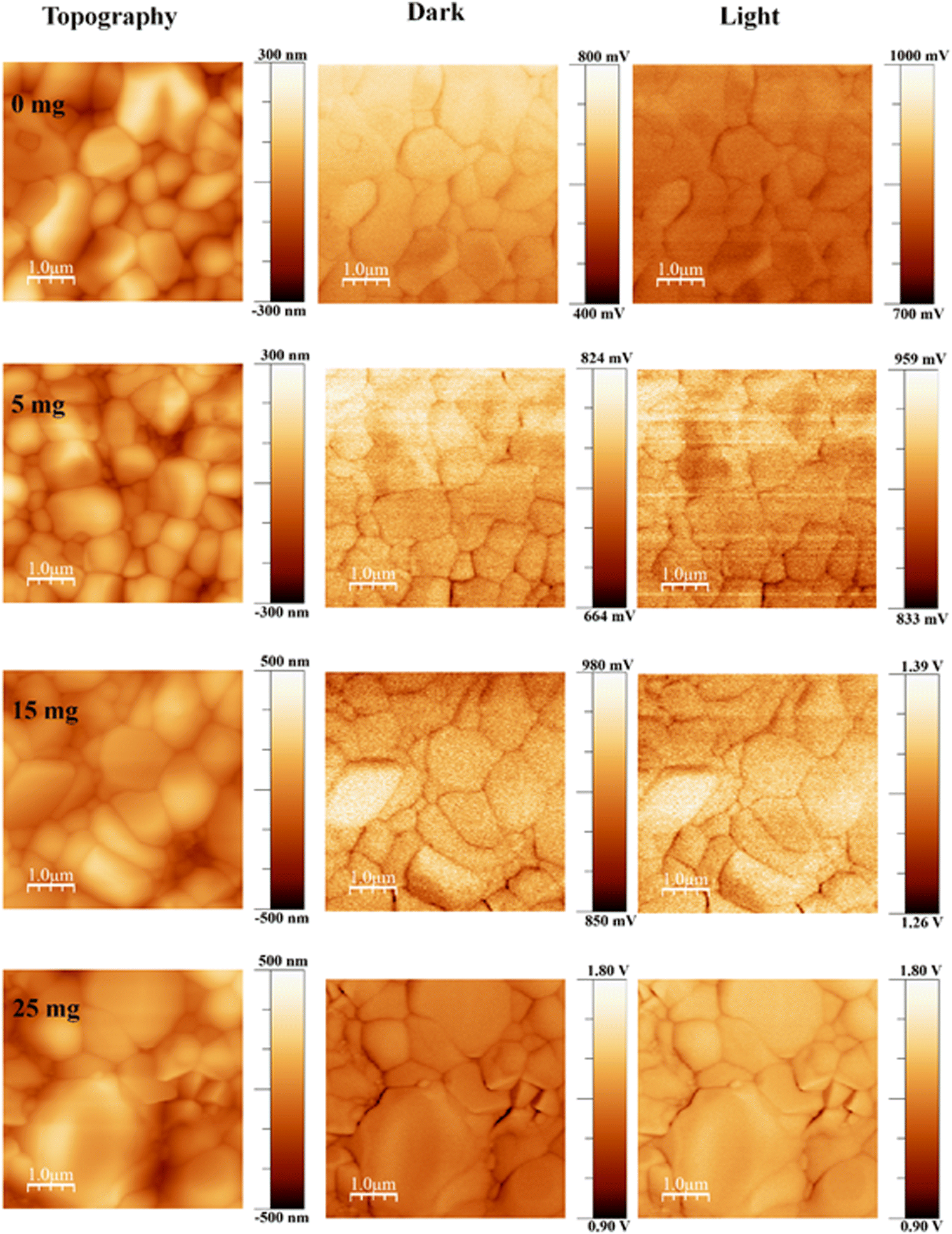 | ||
| Fig. 2 Topography and the corresponding CPD maps of perovskite films with MABr under illumination. | ||
We observed the root-mean-square roughness (RMS) values of 56.68, 62.66, 90.83, and 114.77 nm for 0 mg, 5 mg, 15 mg, and 25 mg MABr-perovskite films, respectively. For the 0 mg film, the flat grains show a lower CPD (∼40 mV) than the rounded ones, as shown in Fig. S4 (ESI†), which implies a deeper Fermi level than the rounder grains and a higher work function. This shows that an upward band bending-induced potential barrier to electron transport may exist at the flat grain. Flat grains with a lower CPD are rarely active in the PSCs.61 Upon addition of MABr flat grains, the CPD shows a slightly higher value (∼15 mV) as shown in Fig. S4 (ESI†), which is advantageous for increasing the open circuit voltage of devices and is consistent with the results of the J–V measurement as shown in Table S2 (ESI†). The CPD line profile in Fig. S4 (ESI†) shows that the bare grain has a large variation in CPD, while the 15 mg MABr grain shows almost no change in CPD. This suggests that the grain quality is greatly improved with the MABr addition, which is well consistent with the c-AFM results shown in Fig. 1, where the flat grains have a higher current.
The lowest CPD value is shown by the 0 mg film, indicating that the bare film has a substantially higher work function than the other films. The CPD values of perovskite films dramatically increased after MABr addition, which implies that the work function values of the films were reduced. The enhanced surface potential leads to efficient charge collection and suppression of charge recombination. This is also advantageous for increasing the electron transfer efficiency at the interface between the perovskite and the electron transport layer.62 By deducting the CPD value under light illumination from the CPD value in the dark, we were also able to measure the photovoltage and obtained a photovoltage of 176.4 mV for bare and 418.13 mV for 15 mg MABr-perovskite films. This result is in qualitative agreement with the macroscopic J–V results shown in Table S1 (ESI†), where the 15 mg device has a higher Voc than the bare one. The overall CPD value increase with MABr addition revealed that the MABr modified films exhibited self-passivation and optimized charge carrier transport behavior compared with the bare film.63,64 The variation in the work function of the sample's local surface is reflected in the change in the measured CPD value.65 We observed a CPD of 650 mV for bare and 926 mV for the 15 mg MABr added CsPbBr3 perovskite in the dark, which represents a lowering of work function for the MABr perovskite by 0.276 eV. A lower work function means the valence band of the MABr-perovskite moves from 5.60 eV to 5.32 eV close to the hole transport layer (HTL) poly[bis(4-phenyl)(2,4,6-trimethylphenyl)amine] (PTAA), as shown in Fig. S5 (ESI†),25,56 which facilitates the hole transport to PTAA, improves the device performance and decreases surface recombination.66 Suppressing non-radiative recombination and extending the lifespan of charge carriers depend on defect passivation. Overall perovskite layer conductivity is improved by reduced recombination. The energy levels and band alignment of the CsPbBr3 perovskite can be affected by the addition of MABr. This may cause the valence band edge to move. Changes in the valence band edge can have an impact on how energy levels match with nearby charge transport layers, which can lead to better charge injection and extraction and eventually higher conductivity.
Scanning electron microscopy (SEM) was used to examine the effect of the MABr additive on the morphology of the perovskite layer, as shown in Fig. 3. Bare perovskite films show fewer pinholes, whereas the MABr addition leads to the formation of uniform and compact films. The grain sizes estimated from the SEM images were 580 ± 53 nm, 489 ± 38 nm, 831 ± 65 nm, and 763 ± 33 nm for bare, 5, 15, and 25 mg MABr-perovskite films, respectively. We obtained a higher average grain size for the CsPbBr3 film with 15 mg MABr, resulting in fewer grain boundaries. This is advantageous for obtaining a higher open circuit voltage and short circuit current, which supports our findings in Table S2 (ESI†). After MABr addition, the grain size increased slightly, and the ion exchange results in the final CsPbBr3 product with MABr being supposed to be MAxCs1−xPbBr3 where x is 0.16, 0.47, and 0.78 for 5 mg, 15 mg, and 25 mg MABr, respectively, which is following the shift in peak position from XRD data (Fig. 4). Zhu et al.57 also obtained a flat grain structure. They presented a mixed-bromide halide exchange technique that eliminates the need for low-solubility CsBr by converting the CsPbIBr2 intermediate phase into CsPbBr3 following spin-coating of MABr/CsBr methanol solution.
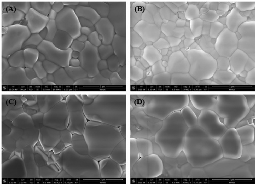 | ||
| Fig. 3 Scanning electron microscopy images of perovskite films with different concentrations of MABr: (A) 0 mg, (B) 5 mg, (C) 15 mg, and (D) 25 mg. | ||
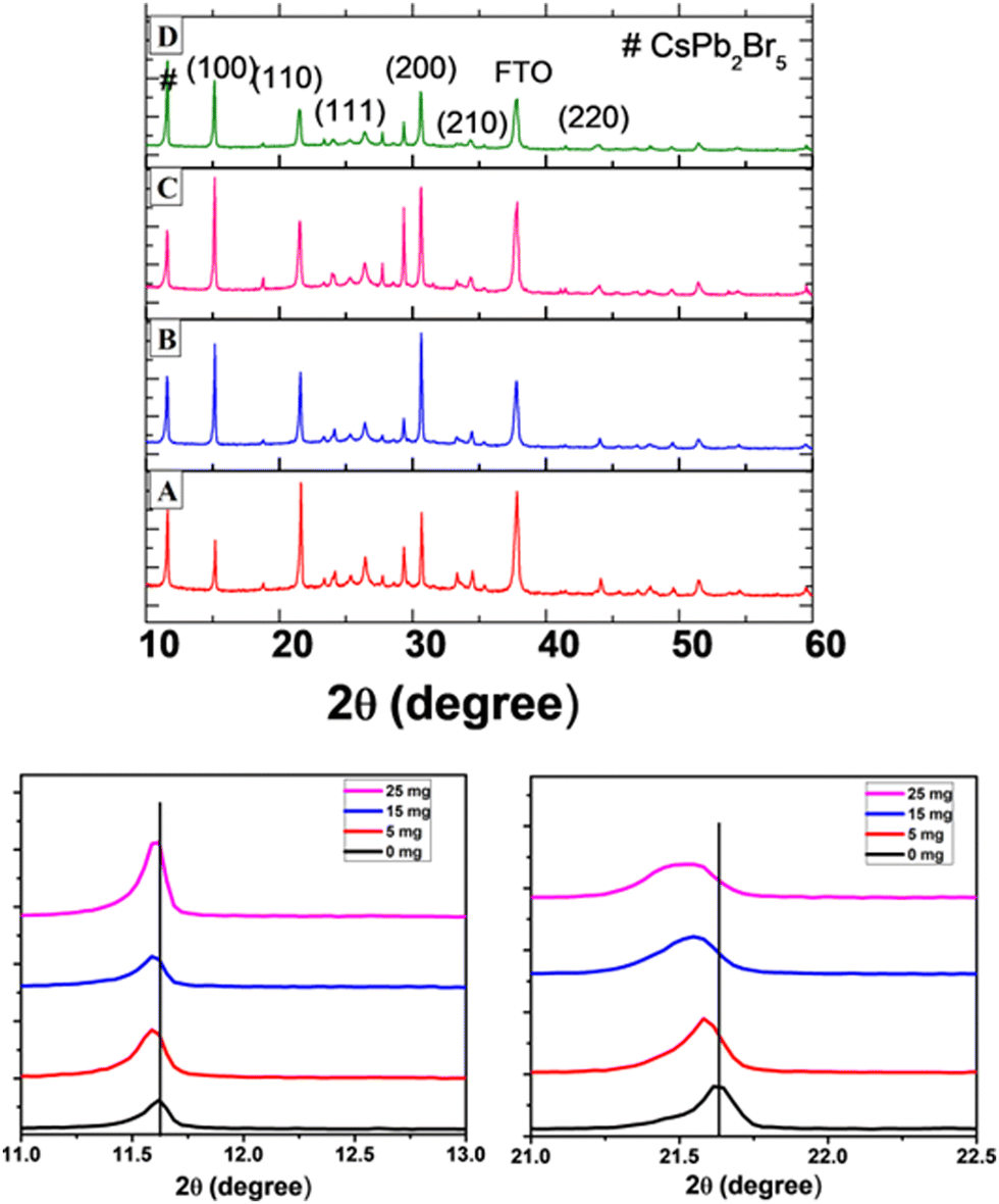 | ||
| Fig. 4 X-ray diffraction patterns of perovskite films with different concentrations of MABr: (A) 0 mg, (B) 5 mg, (C) 15 mg, and (D) 25 mg. The bottom figure shows the zoomed-in view of the diffraction peak of CsPb2Br5 and the (110) plane. | ||
X-ray diffraction (XRD) was performed on the perovskite samples with and without the MABr additive. The XRD pattern of the CsPbBr3 perovskite is shown in Fig. 4 with characteristic peaks at 15.20°, 20.7°, 24.1°, 30.7°, 34.5°, and 43.8° corresponding to the (100), (110), (111), (200), (210), and (220) planes of cubic CsPbBr3, respectively.36,67 We found that there is a shift in peaks with MABr towards a lower angle compared to the bare film, as a partial replacement of Cs+ with larger MA+, which represents lattice expansion. This suggests that MA+ cations are incorporated into the perovskite crystal,33 forming an intermediate phase,68 which could be ascribed to the formation of an alloy phase of MAxCs1−xPbBr3 where x is 0.16, 0.47, and 0.78 for 5 mg, 15 mg, and 25 mg MABr, respectively. The diffraction peaks at 26.4° and 37.8° represent FTO, and the peak at 11.6° is attributed to the CsPb2Br5 phase.38 It represents the excess amount of PbBr2 in the perovskite film, and this is generally observed for the two-step deposition process of the CsPbBr3 perovskite film, as reported previously.69,70 The CsPb2Br5 phase is suppressed with the addition of MABr until 15 mg, and after that, it again increases.
Fig. 5 show the absorbance edge of perovskite films and it is almost the same with negligible changes upon MABr addition. Fig. 6 shows the PL spectra of CsPbBr3 films with MABr which show that the PL peak is significantly reduced with 15 mg MABr. This shows that, at this doping concentration, the CsPbBr3 light-absorbing layer is more efficient for charge extraction.23
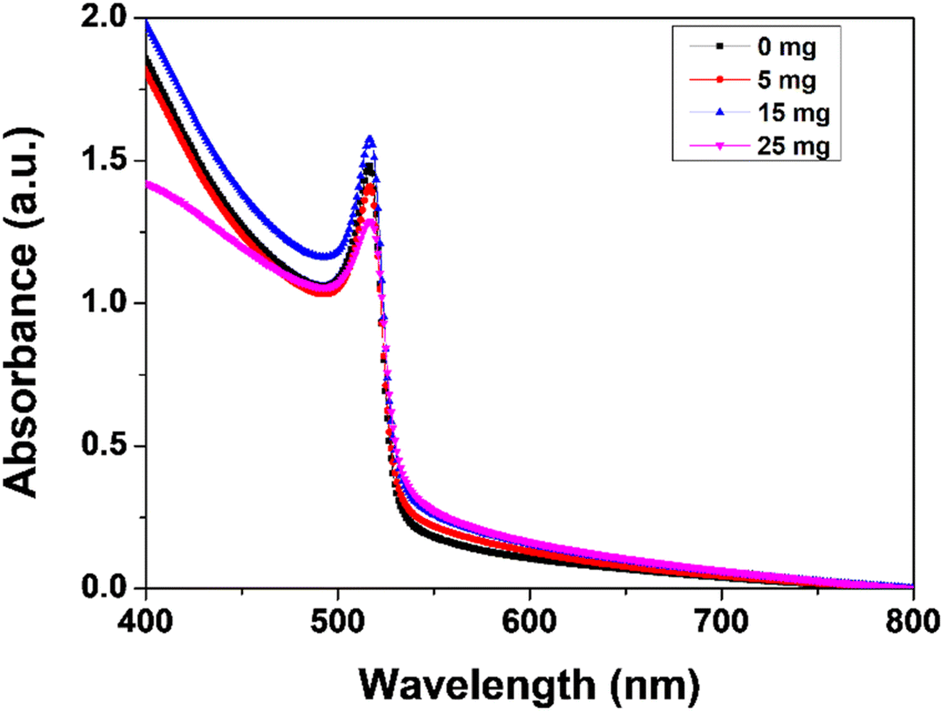 | ||
| Fig. 5 Absorbance spectra of CsPbBr3 with MABr. | ||
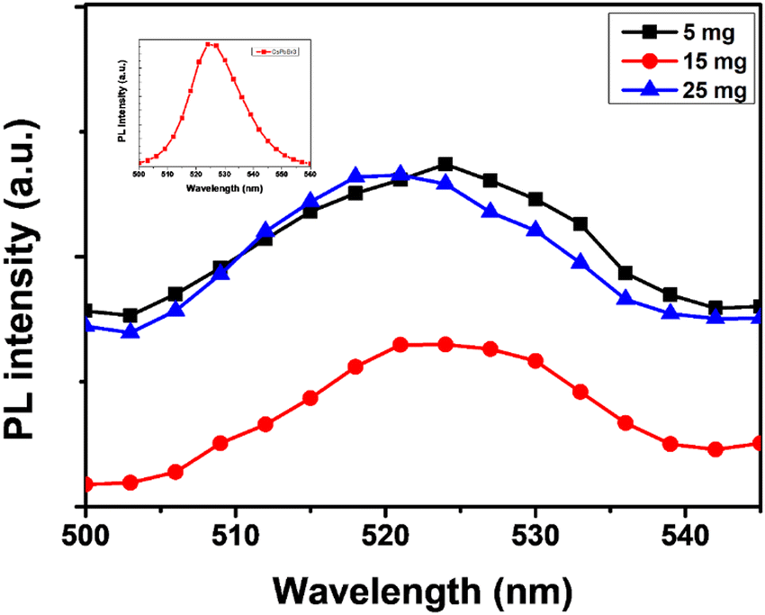 | ||
| Fig. 6 PL spectra of CsPbBr3 with MABr. The inset shows the PL spectra of the bare perovskite film. | ||
To validate the successful doping of MA+ ions in the perovskite layer, X-ray photoelectron spectroscopy (XPS) was carried out as shown in Fig. 7. The N 1s spectra demonstrate that MA+ ions are present in the perovskite layer. From the XPS spectra, a shift was observed in the peak positions of Pb 4f and Br 3d to higher binding energies after the addition of MABr, which is mainly attributed to the redistributed electron density caused by the different binding interactions of the MA+ ion with Pb and Br. Cs 3d shows obviously less shift.26,56 The atomic% deduced from XPS is shown in Table S1 (ESI†). With the atomic percentages of nitrogen and cesium, one can compute the ratio of MA to Cs. The quantity of nitrogen directly indicates the presence of MA cations because it is specific to MA cations and it was absent in the bare perovskite.
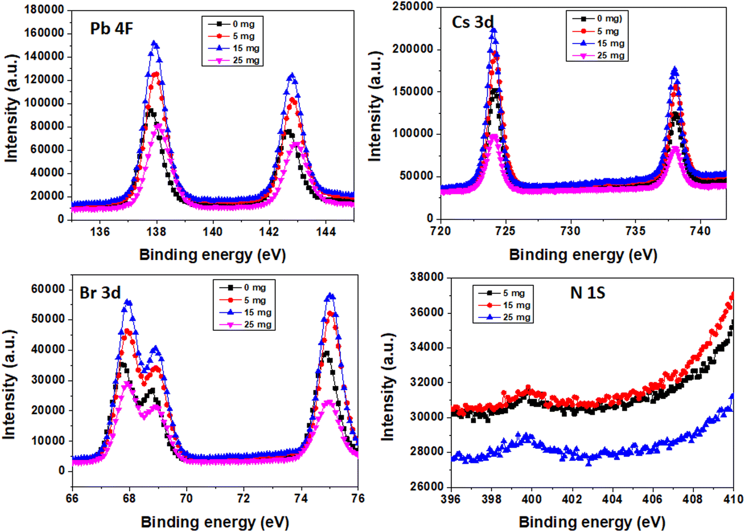 | ||
| Fig. 7 XPS spectra of Pb 4f, Cs 3d, Br 3d and N 1s elements of perovskite films. | ||
Under typical 1 sun conditions, the photovoltaic performance was examined using current density–voltage (J–V) characteristics. Fig. 8 shows the J–V characteristics of the best-performing devices with varying MABr. Table S2 (ESI†) shows the average values of the photovoltaic performance parameters of glass/FTO/c-TiO2/m-TiO2/perovskite/PTAA/Au solar cells without and with MABr. For the bare film, the grains are inefficient for charge transfer as shown in Fig. 1, which results in poor overall performance of the device, while MABr-added devices show enhancements in all device parameters, especially for optimized 15 mg MABr, which can be mainly attributed to the increased conductivity of flat grains, and enhanced carrier transport by MABr. Due to the improved charge carrier transport efficiency as shown in the c-AFM current map (Fig. 1), the efficiency of PSCs is improved. The MABr also improves hole transfer to the PTAA, as shown in Fig. S4 (ESI†), which further explains the improved performance of PSCs with additives. The slight increment in Voc and FF is attributed to the inhibited carrier recombination due to the MABr. The Jsc enhancement is attributed to the enhanced light harvesting by the CsPbBr3 perovskite layer with MABr addition, which facilitates charge separation and transportation, hence improving Jsc. After the optimal addition of 15 mg MABr, the PCE starts to decrease, which probably indicates the recombination and degradation of crystalline quality induced by excess MABr.
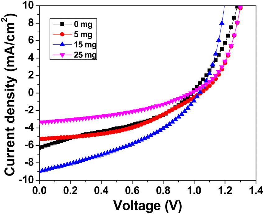 | ||
| Fig. 8 J–V characteristics of CsPbBr3 devices with MABr. | ||
Conclusions
Here, our goal was to comprehend how MABr addition affected the electrical characteristics of perovskite grains. We suggest that adding MABr to the precursor solution enhances the conductivity of grains based on the results from c-AFM experiments. c-AFM and KPFM measurements show that MABr addition improves the optoelectronic properties of perovskite grains in addition to charge carrier transport and hence increases the PCE. KPFM demonstrated that the valence band of the MABr-perovskite moves close to the PTAA, which improves the hole transfer from the perovskite to the PTAA layer.We demonstrated the benefits of the incorporation of MABr into the CsBr solution to form high optoelectronic quality CsPbBr3 grains. The photovoltaic properties of devices were improved with the addition of MABr to precursor solutions. This work presents a simple method to enhance the optoelectronic properties of perovskite absorber layers and thus PSCs.
Data availability
The data supporting this article have been included as part of the ESI.†Conflicts of interest
There are no conflicts to declare.Acknowledgements
We are grateful to Juergen Jopp and Dr Natalya Froumin for their assistance with SPM and XPS measurements. This research was supported by the Ministry of Science and Technology, Israel, and the Department of Science and Technology, India, through grant number 3-17411. SG and SM thank the DST-India for the Indo-Israeli Joint Research Project (DST/INT/ISR/P-28/2020) for financial support. DA thanks the Ministry of Education for the fellowship.References
- T. Miyasaka, A. Kojima, K. Teshima and Y. Shirai, J. Am. Chem. Soc., 2009, 131, 6050–6051 CrossRef PubMed.
- H. S. Kim, C. R. Lee, J. H. Im, K. B. Lee, T. Moehl, A. Marchioro, S. J. Moon, R. Humphry-Baker, J. H. Yum, J. E. Moser, M. Grätzel and N. G. Park, Sci. Rep., 2012, 2, 591 CrossRef PubMed.
- N. J. Jeon, H. Na, E. H. Jung, T. Y. Yang, Y. G. Lee, G. Kim, H. W. Shin, S. Il Seok, J. Lee and J. Seo, Nat. Energy, 2018, 3, 682–689 CrossRef CAS.
- J. Park, J. Kim, H.-S. Yun, M. J. Paik, E. Noh, H. J. Mun, M. G. Kim, T. J. Shin and S. Il Seok, Nature, 2023, 616, 724–730 CrossRef CAS PubMed.
- T. P. Gujar and M. Thelakkat, Energy Technol., 2016, 4, 449–457 CrossRef CAS.
- J. Burschka, N. Pellet, S. J. Moon, R. Humphry-Baker, P. Gao, M. K. Nazeeruddin and M. Grätzel, Nature, 2013, 499, 316–319 CrossRef CAS PubMed.
- Z. Zhao, X. Chen, H. Wu, X. Wu and G. Cao, Adv. Funct. Mater., 2016, 26, 3048–3058 CrossRef CAS.
- M. Saliba, T. Matsui, J. Y. Seo, K. Domanski, J. P. Correa-Baena, M. K. Nazeeruddin, S. M. Zakeeruddin, W. Tress, A. Abate, A. Hagfeldt and M. Grätzel, Energy Environ. Sci., 2016, 9, 1989–1997 RSC.
- T. Singh, M. Ikegami and T. Miyasaka, ACS Appl. Energy Mater., 2018, 1, 6741–6747 CrossRef CAS.
- F. Wang, W. Geng, Y. Zhou, H. Fang, C. Tong, M. A. Loi, L. Liu and N. Zhao, Adv. Mater., 2016, 28, 9986–9992 CrossRef CAS PubMed.
- C. Park, H. Ko, D. H. Sin, K. C. Song and K. Cho, Adv. Funct. Mater., 2017, 27, 1703546 CrossRef.
- X. Liu, J. Wu, Q. Guo, Y. Yang, H. Luo, Q. Liu, X. Wang, X. He, M. Huang and Z. Lan, J. Mater. Chem. A, 2019, 7, 11764–11770 RSC.
- C. Lin, J. Lee, J. Kim, T. J. Macdonald, J. Ngiam, B. Xu, M. Daboczi, W. Xu, S. Pont, B. Park, H. Kang, J. Kim, D. J. Payne, K. Lee, J. R. Durrant and M. A. Mclachlan, Adv. Funct. Mater., 2020, 30, 1906763 CrossRef CAS.
- C. Lin, F. De Rossi, J. Kim, J. Baker, J. Ngiam, B. Xu, S. Pont, N. Aristidou, S. A. Haque, T. Watson, A. Mclachlan and J. R. Durrant, J. Mater. Chem. A, 2019, 7, 3006–3011 RSC.
- X. Li, J. Luo, M. Ibrahim Dar, C. Yi, M. Tschumi, H. Han, M. Grätzel, S. M. Zakeeruddin and M. K. Nazeeruddin, Nat. Chem., 2015, 7, 703–711 CrossRef CAS PubMed.
- M. Abdi-jalebi, Z. Andaji-garmaroudi, S. Cacovich, C. Stavrakas, B. Philippe, E. M. Hutter, A. J. Pearson, S. Lilliu, T. J. Savenije, J. M. Richter, M. Alsari, P. Edward, H. Rensmo, G. Divitini, C. Ducati, R. H. Friend and S. D. Stranks, Nature, 2018, 555, 497 CrossRef CAS PubMed.
- J. Dagar, K. Hirselandt, A. Merdasa, A. Czudek, R. Munir, F. Zu, N. Koch, T. Dittrich and E. L. Unger, Sol. RRL, 2019, 3, 1900088 CrossRef.
- C. Y. Chang, C. Y. Chu, Y. C. Huang, C. W. Huang, S. Y. Chang, C. A. Chen, C. Y. Chao and W. F. Su, ACS Appl. Mater. Interfaces, 2015, 7, 4955–4961 CrossRef CAS PubMed.
- A. Fakharuddin, M. Seybold, A. Agresti, S. Pescetelli, F. Matteocci, M. I. Haider, S. T. Birkhold, H. Hu, R. Giridharagopal, M. Sultan, I. M. Sero, A. Di Carlo and L. Schmidt-Mende, ACS Appl. Mater. Interfaces, 2018, 10, 42542–42551 CrossRef CAS PubMed.
- D. J. Fairfield, H. Sai, A. Narayanan, J. V. Passarelli, M. Chen, J. Palasz, L. C. Palmer, M. R. Wasielewski and S. I. Stupp, J. Mater. Chem. A, 2019, 7, 1687–1699 RSC.
- D. Wang, L. Zhang, K. Deng, W. Zhang, J. Song, J. Wu and Z. Lan, Energy Technol., 2018, 6, 2380–2386 CrossRef CAS.
- C. S. Pathak, G. Paramasivam, F. Mathies, K. Hirselandt, V. S. Der, O. Maus, J. Dagar, C. Klimm, E. Unger and I. Visoly-fisher, ACS Appl. Energy Mater., 2022, 5, 4085–4095 CrossRef CAS.
- H. Choi, H. Lim, H. Kim, J. Lim, M. Park, C. S. Pathak and S. Song, J. Mater. Chem. A, 2023, 11, 16363–16369 RSC.
- C. S. Pathak, H. Choi, H. Kim, J. Lim, S. K. Cho, D. S. Ham and S. Song, Sol. RRL, 2024, 8, 2300860 CrossRef.
- H. Guo, Y. Pei, J. Zhang, C. Cai, K. Zhou and Y. Zhu, J. Mater. Chem. C, 2019, 7, 11234–11243 RSC.
- D. Wang, W. Li, Z. Du, G. Li, W. Sun, J. Wu and Z. Lan, J. Mater. Chem. C, 2020, 8, 1649–1655 RSC.
- S. Chen, X. Liu, Z. Wang, W. Li, X. Gu, J. Lin, T. Yang, X. Gao and A. K. K. Kyaw, Adv. Energy Sustainability Res., 2021, 2, 2000099 CrossRef CAS.
- D. Wang, W. Li, Z. Du, G. Li, W. Sun, J. Wu and Z. Lan, ACS Appl. Mater. Interfaces, 2020, 12, 10579–10587 CrossRef CAS PubMed.
- Y. Li, J. Duan, H. Yuan, Y. Zhao, B. He and Q. Tang, Sol. RRL, 2018, 2, 1800164 CrossRef.
- Y. Ren, N. Zhang, Z. Arain, M. Mateen, J. Chen, Y. Sun and Z. Li, J. Power Sources, 2020, 475, 228676 CrossRef CAS.
- J. Zhu, B. He, Z. Gong, Y. Ding, W. Zhang, X. Li, Z. Zong, H. Chen and Q. Tang, ChemSusChem, 2020, 13, 1834–1843 CrossRef CAS PubMed.
- J. Lou, B. Cai, Y. Wu, Y. Lv, X. Liu, W. Zhang and Y. Qin, J. Alloys Compd., 2021, 872, 159601 CrossRef CAS.
- Y. Zhao, Y. Wang, J. Duan, X. Yang and Q. Tang, J. Mater. Chem. A, 2019, 7, 6877–6882 RSC.
- D. Huang, P. Xie, Z. Pan, H. Rao and X. Zhong, J. Mater. Chem. A, 2019, 7, 22420–22428 RSC.
- S. Yu, A. F. Akbulatov, L. A. Frolova, S. A. Tsarev, P. A. Troshin and K. J. Stevenson, Sol. Energy Mater. Sol. Cells, 2017, 171, 205–212 CrossRef.
- X. Liu, X. Tan, Z. Liu, H. Ye, B. Sun, T. Shi, Z. Tang and G. Liao, Nano Energy, 2019, 56, 184–195 CrossRef CAS.
- W. Zhang, X. Liu, B. He, J. Zhu, X. Li, K. Shen, H. Chen, Y. Duan and Q. Tang, ACS Appl. Mater. Interfaces, 2020, 12, 36092–36101 CrossRef CAS PubMed.
- X. Cao, G. Zhang, L. Jiang, Y. Cai, Y. Gao, W. Yang, X. He, Q. Zeng, G. Xing, Y. Jia and J. Wei, ACS Appl. Mater. Interfaces, 2020, 12, 5325–5931 Search PubMed.
- X. Zhang, Z. Jin, J. Zhang, D. Bai, H. Bian, K. Wang, J. Sun, Q. Wang and S. F. Liu, ACS Appl. Energy Mater., 2018, 10, 7145–7154 CrossRef CAS PubMed.
- J. Zhu, B. He, Z. Gong, Y. Ding, W. Zhang and X. Li, ChemSusChem, 2020, 13, 1834–1843 CrossRef CAS PubMed.
- X. Li, Y. Tan, H. Lai, S. Li, Y. Chen, S. Li, P. Xu and J. Yang, ACS Appl. Mater. Interfaces, 2019, 11, 23746–29752 Search PubMed.
- M. Kulbak, S. Gupta, N. Kedem, I. Levine, T. Bendikov, G. Hodes and D. Cahen, J. Phys. Chem. Lett., 2016, 7, 167–172 CrossRef CAS PubMed.
- J. S. Yun, A. Ho-baillie, S. Huang, S. H. Woo, Y. Heo, J. Seidel, F. Huang, Y. Cheng and M. A. Green, J. Phys. Chem. Lett., 2015, 6, 875–880 CrossRef CAS PubMed.
- J. J. Li, J. Y. Ma, Q. Q. Ge, J. S. Hu, D. Wang and L. J. Wan, ACS Appl. Mater. Interfaces, 2015, 7, 28518–28523 CrossRef CAS PubMed.
- S. Y. Leblebici, L. Leppert, Y. Li, S. E. Reyes-Lillo, S. Wickenburg, E. Wong, J. Lee, M. Melli, D. Ziegler, D. K. Angell, D. F. Ogletree, P. D. Ashby, F. M. Toma, J. B. Neaton, I. D. Sharp and A. Weber-Bargioni, Nat. Energy, 2016, 1, 16093 CrossRef CAS.
- J. Xu, A. Buin, A. H. Ip, W. Li, O. Voznyy, R. Comin, M. Yuan, S. Jeon, Z. Ning, J. J. Mcdowell, P. Kanjanaboos, J. Sun, X. Lan, L. N. Quan, D. H. Kim, I. G. Hill, P. Maksymovych and E. H. Sargent, Nat. Commun., 2015, 6, 7081 CrossRef CAS PubMed.
- A. Gomez, S. Sanchez, M. Campoy-quiles and A. Abate, Nano Energy, 2018, 45, 94–100 CrossRef CAS.
- J. Hieulle, C. Stecker, R. Ohmann, L. K. Ono and Y. Qi, Small Methods, 2018, 16, 1700295 CrossRef.
- Y. Harari, C. S. Pathak and E. Edri, Nanoscale, 2023, 15, 4951–4961 RSC.
- H. Si, S. Zhang, S. Ma, Z. Xiong, A. Kausar, Q. Liao, Z. Zhang, A. Sattar, Z. Kang and Y. Zhang, Adv. Energy Mater., 2020, 10, 1903922 CrossRef CAS.
- C. S. Pathak, Opt. Mater., 2022, 133, 113012 CrossRef CAS.
- C. S. Pathak, B.-J. Chang and S. Song, Dyes Pigm., 2023, 218, 111469 CrossRef CAS.
- Y. Kutes, Y. Zhou, J. L. Bosse, J. Steffes, N. P. Padture and B. D. Huey, Nano Lett., 2016, 16, 3434–3441 CrossRef CAS PubMed.
- J. Yang, X. Liu, Y. Zhang, X. Zheng, X. He, H. Wang, F. Yue, S. Braun, J. Chen, J. Xu, Y. Li and Y. Jin, Nano Energy, 2018, 54, 218–226 CrossRef CAS.
- Y. Shao, Y. Fang, T. Li, Q. Wang, Q. Dong, Y. Deng, Y. Yuan, H. Wei, M. Wang, A. Gruverman, J. Shield and J. Huang, Energy Environ. Sci., 2016, 9, 1752–1759 RSC.
- Y. Pei, H. Guo, Z. Hu, J. Zhang and Y. Zhu, J. Alloys Compd., 2020, 835, 155283 CrossRef CAS.
- W. Zhu, X. Yao, S. Shi, Z. Zhang, Z. Song, P. Gao and T. Wang, ACS Appl. Energy Mater., 2023, 6, 9798–9804 CrossRef CAS.
- J. W. Lee, S. H. Bae, Y. T. Hsieh, N. De Marco, M. Wang, P. Sun and Y. Yang, Chem, 2017, 3, 290–302 CAS.
- Y. Wang, Z. Hu, C. Gao, C. Yang, J. Zhang and Y. Zhu, Adv. Mater. Interfaces, 2020, 7, 1901521 CrossRef CAS.
- C. Yang, P. Du, Z. Dai, H. Li, X. Yang and Q. Chen, ACS Appl. Mater. Interfaces, 2019, 11, 14044–14050 CrossRef CAS PubMed.
- A. Dymshits, A. Henning, G. Segev, Y. Rosenwaks and L. Etgar, Sci. Rep., 2015, 5, 8704 CrossRef CAS PubMed.
- H. Zeng, L. Li, F. Liu, M. Li, S. Zhang, X. Zheng, L. Luo, S. You, Y. Zhao, R. Guo, Z. Gong, R. Huang, Z. Li, T. Wang, X. L. Yi Cui and Y. Rong, Adv. Energy Mater., 2022, 12, 2102820 CrossRef CAS.
- A. F. Castro-Méndez, J. Hidalgo and J. P. Correa-Baena, Adv. Energy Mater., 2019, 9, 1901489 CrossRef.
- D. S. Lee, J. S. Yun, J. Kim, A. M. Soufiani, S. Chen, Y. Cho, X. Deng, J. Seidel, S. Lim, S. Huang and A. W. Y. Ho-Baillie, ACS Energy Lett., 2018, 3, 647–654 CrossRef CAS.
- X. Liu, L. Shi, J. Huang, Z. Liu, P. Zhang, J. S. Yun, A. M. Soufiani, J. Seidel, K. Sun, Z. Hameiri, J. A. Stride, Y. Zhang, M. A. Green, H. Lin and X. Hao, Sol. RRL, 2019, 3, 1800338 CrossRef.
- L. Zhang, T. Guo, B. Liu, D. Du, S. Xu, H. Zheng, L. Zhu, X. Pan and G. Liu, ACS Appl. Mater. Interfaces, 2022, 14, 19614–19622 CrossRef CAS PubMed.
- X. Chang, W. Li, L. Zhu, H. Liu, H. Geng, S. Xiang and J. Liu, ACS Appl. Mater. Interfaces, 2016, 8, 33649–33655 CrossRef CAS PubMed.
- J. Zhang, Z. Wang, A. Mishra, J. Zhang, Z. Wang, A. Mishra, M. Yu, M. Shasti, W. Tress, A. Agarwalla, Z. Wang, W. Xiang, L. Emsley and Z. Zhang, Joule, 2020, 4, 222–234 CrossRef CAS.
- H. Li, G. Tong, T. Chen, H. Zhu, G. Li, Y. Chang, L. Wang and Y. Jiang, J. Mater. Chem. A, 2018, 6, 14255–14261 RSC.
- Z. Liu, B. Sun, X. Liu, J. Han, H. Ye, T. Shi, Z. Tang and G. Liao, Nano-Micro Lett., 2018, 10, 1–13 CrossRef PubMed.
Footnote |
| † Electronic supplementary information (ESI) available: Line section analysis, EDX, chronoamperometric plots, CPD map of perovskite films, energy diagram, and chronoamperometric plots and photovoltaic parameters of devices. See DOI: https://doi.org/10.1039/d4ya00487f |
| This journal is © The Royal Society of Chemistry 2024 |