
 Open Access Article
 This Open Access Article is licensed under a Creative Commons Attribution-Non Commercial 3.0 Unported Licence
Novel 2D structural material design: carbon–aluminium–boron nitrides (CC–(Al–B)N) and carbon–aluminium–gallium nitrides (CC–(Al–Ga)N) for optical and optoelectronic system applications
V. W.
Elloh
 *ab,
D. E.
Anderson
a,
D.
Abbeyquaye
a,
D. F.
Ofosuhene
a,
I.
Arhin
a,
Edwin Okoampa
Boadu
a,
A.
Yaya
c and
Eric K. K.
Abavare
d
*ab,
D. E.
Anderson
a,
D.
Abbeyquaye
a,
D. F.
Ofosuhene
a,
I.
Arhin
a,
Edwin Okoampa
Boadu
a,
A.
Yaya
c and
Eric K. K.
Abavare
d
aDepartment of Biomedical Engineering, Koforidua Technical University, Koforidua, Ghana. E-mail: vanw.elloh@ktu.edu.gh
bDepartment of Physics, University of Petroleum and Energy Studies (UPES), Dehradun, India
cDepartment of Materials Science and Engineering, University of Ghana, Legon, Ghana
dDepartment of Physics, KNUST, Kumasi, Ghana
First published on 8th July 2024
Abstract
In this paper, two new 2D hybrid nanoheterostructures, namely AlN:CC:GaN:CC and AlN:CC:BN:CC, have been designed through density functional theory (DFT) methods. Their structural, electronic and optical properties have been sequentially investigated by first principles calculations. Phonon spectral dispersion calculations show that the novel materials have stable configurations. The results reveal that AlN:CC:GaN:CC is a direct band gap semiconducting material, with a band gap of 1.20 eV, which is desirable for optoelectronic applications. On the other hand, AlN:CC:BN:CC is an indirect band gap semiconducting nanoheterostructure with a band gap value of 0.98 eV, which is suitable for high-performance nanoelectronic device applications, energy conversion and energy storage. These materials have shown large optical absorption for visible and UV frequencies. They display anisotropic optical properties along the in-plane and out-of-plane directions. The results suggest the two novel 2D nanoheterostructures as promising candidates for potential applications in nano-electronics and opto-electronics.
1. Introduction
With the advent of graphene discovery coupled with the successes achieved in several realms of innovative research,1–7 researchers have rushed to exploit and study two-dimensional materials. Silicene, germanene and phosphorene are among 2D materials that have surfaced in the materials world in the mid-90s and captivated considerable attention from scientists.8–15 Materials of 2D geometry possess fascinating properties, such as flexibility and high mobility due to decreased dimensionality.16Copious classes of two-dimensional materials have been concocted, such as elemental atomic sheets, hexagonal boron nitride (h-BN), transition metal dichalcogenides, 2D metal oxides, metal carbides and nitrides. To date, colonies of 2D materials are continuously emanating, giving rise to novel terrains and prospective promising unlimited scientific and technological machinations. Multifarious molecular structures can be engineered with different doping patterns within the graphene frame. Based on the doping pattern, each nanoarchitecture with different electronic band structures and energy band gap values can be realized. The tunability of the band gap and band characteristics are crucially important as they regulate how the material responds to incident light and also participates in chemical reactions.
Materials research is noted to be associated with dimensionality. This refers to both the structural features of the materials and the determination of many other properties.17 When graphene was isolated from bulk graphite with success, it was realized that it possessed myriad outstanding physical properties. Among them are very fast electron transition time, flexibility, ballistic transport of charge carriers, toughness, light-weight, etc. Based on the above prospects, the attention of numerous research societies in 2D structural systems found a new turn.6,7 2D geometry and its associated unique electronic and optical properties, high mechanical strength and flexibility are indispensable for electronic industry implementations.18–21
Atomically thin 2D structures have found dominance in issues of deeply basic and state-of-the-art research.22–27 As dimensions are reduced greatly with their accompanied weak dielectric screening, the opto-electronic response of the materials at room temperature is dominated by strongly bound electron–hole pairs or excitons.28 2D materials are mostly attractive for very high absorbance. The optical band gaps of these 2D materials are found in the visible to the near-infrared region of the electromagnetic spectrum.29,30 Photovoltaic, solar cell,31,32 photodetector, and light-emitting diode33–38 manufacturing industries are vibrant markets for 2D materials. Optoelectronic, photonic and MEMS industries, who are envisaged as the leading giants in technology, rely mightily on 2D nanomaterials.
2D materials coming from light and nonmetal atoms are crucial for designing requisite and desired electromechanical functional properties. They give rise to conjugated structures. This is critical for tailoring novel properties to electronic band gap engineering in 2D nanostructures. In the current paper, we employ first-principles methods to design a technologically fascinating two-dimensional nanostructure with a visible-light range tunable band gap for nano-opto-electronics, nano-optics and electronic-based device industries.
2. Theoretical methods
Ab-initio calculations were performed within the density functional theory (DFT) framework using the plane wave self-consistent field (PWSCF) basis sets as implemented in the Quantum Espresso code.39 We employed the generalized gradient approximation (GGA) of Perdew, Burke and Ernzerhof (PBE).40 The Kohn–Sham orbitals were expanded in a plane-wave basis set. The Vanderbilt ultrasoft pseudopotentials scheme41 was employed. The ultrasoft pseudopotentials represent the interaction between ionic cores and the valence electrons. We adopted the supercell model for the nanoarchitectures and a unit cell geometry with a vacuum space of 15 Å thick in the z-direction was allowed to ensure negligible interactions between the supercells and their periodic images. vdW interactions are known to be significant in carbon nano systems; therefore, Grimme's D3 correction term42–45 was applied to include the van der Waals (vdW) interactions. The cut-off energy for plane wave expansion was set to 80 Ry. The charge density cut-off was set at 240 Ry. Integration over the Brillouin zone was carried out using the Monkhorst–Pack scheme46 with a 12 × 12 × 1 mesh of k-points. Occupation numbers were treated according to the Methfessel–Paxton47 scheme with a broadening of 0.003 Ry. Atomic positions and cell parameters were fully relaxed at an energy convergence of 1 × 10⁻⁶ eV and force convergence of 0.030 eV Å−1.Time-dependent density functional perturbation theory (TDDFPT) was employed in the computations of optical absorption spectra of the modelled structures. We performed self-consistent-field ground-state calculations at the equilibrium structure using the standard plane-wave program. In this case, the k-point sampling is restricted to the Γ-point only.
Lattice-dynamical calculations for the phonon spectrum and density of states were performed within the framework of the self-consistent density functional perturbation theory (DFPT).48 Plane wave cut-off energies of 30 and 650 Ry were used to describe the wave functions and charge density, respectively. Such a high charge density cut-off is necessary to keep the errors in vibrational frequencies minimal. In order to understand the detailed features of the phonon spectra, force constants were obtained on a 4 × 4 × 4 q-point mesh. The dynamical matrices at arbitrary wave vectors were obtained using Fourier transform based interpolations.
3. Results and discussion
3.1 Geometrical structure
In this section, we analyze the geometry and structural stability of the two nanoheterostructures designed. Fig. 1 shows pictorial representations of AlN:CC:GaN:CC (hereafter refer to as nanoarchitecture-A) and AlN:CC:BN:CC (hereafter refer to as nanoarchitecture-B) used in the current study. To obtain nanoarchitecture-A, alternative carbon (CC) layers of a supercell consisting of 32-CC-atoms were replaced with aluminium nitride (AlN) and gallium nitride (GaN) atoms as portrayed in Fig. 1(a). In a likewise manner, carbon (CC) layers were substituted for in turn using AlN and BN atoms to get nanoarchitecture-B as delineated by Fig. 1(b).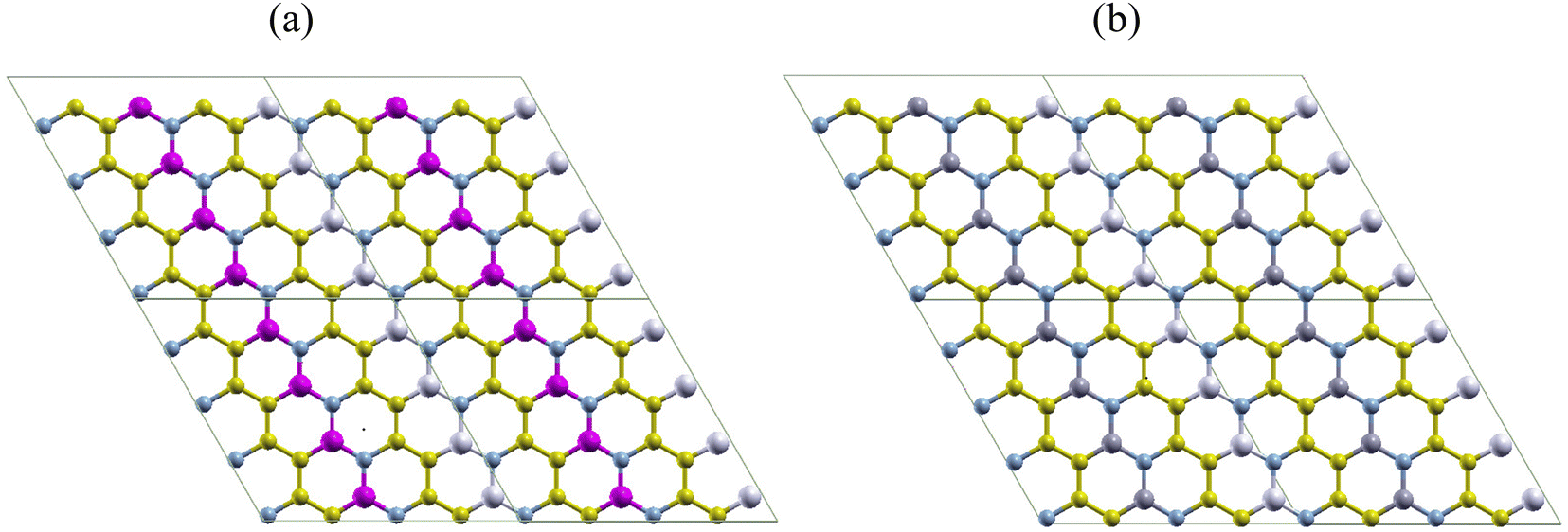 | ||
| Fig. 1 Simulated nanoheterostructures of the (a) AlN:CC:GaN:CC (hereafter refer to as nanoarchitecture-A), and (b) AlN:CC:BN:CC (hereafter refer to as nanoarchitecture-B) configurational modes. The graphene structure was altered using AlN, BN, and GaN layers. A carbon-atom concentration of 50% is maintained in both modes. Structures (a) and (b) each depict a 2 × 2-unit cell. Colour code for the atoms: for (a) blue – nitrogen; gold – carbon; pink – gallium; white – aluminium. For (b) blue – nitrogen; gold – carbon; gray – boron; white – aluminium. | ||
The thermodynamic feasibility of the AlN–CC–GaN–CC & AlN–CC–BN–CC modes are predicted based on the formation energy values obtained from relation (1) below.
| ΔE = E(CC:AlN:B/GaN) − NCEC − NAlEAl − NNEN − N(B/Ga)E(B/Ga) | (1) |
The formation energies per atom for the nanoarchitectures are displayed in Table 1. Comparison between the AlN:CC:GaN:CC and AlN:CC:BN:CC nanoarchitectures reveals that the AlN:CC:GaN:CC configuration is thermodynamically more feasible compared to the AlN:CC:BN:CC configuration. The two newly fabricated 2D materials registered negative energy values, implying that AlN:CC:GaN:CC and AlN:CC:BN:CC are obtainable thermodynamically. Furthermore, the formation energy per atom was quantified individually for the pristine structures GaN, AlN and BN. The respective formation energy per atom values obtained in our computations are −0.668, −1.596 and −1.473 eV. The nature of these computed values shows that the new structures designed are more stable compared with the pristine structures.
| Doping (%) | FE/A (eV) | |
|---|---|---|
| AlN:CC:GaN:CC | 0.500 | −8.619 |
| AlN:CC:BN:CC | 0.500 | −8.876 |
The values in Table 2 show some level of increase in volume of the 2D CC supercell when AlN, BN and GaN layers are incorporated into the sheet. The volumes for AlN:CC:GaN:CC and AlN:CC:BN:CC have seen dramatic changes from 582.091 Å3 initially for graphene to 837.708 and 802.472 Å3, respectively.
| a (Å) | b (Å) | V (Å3) | E g (eV) | |
|---|---|---|---|---|
| CC | 9.878 | 8.556 | 582.091 | 0.00 |
| AlN:CC:GaN:CC | 12.570 | 9.622 | 837.708 | 1.20 |
| AlN:CC:BN:CC | 13.139 | 8.748 | 802.472 | 0.98 |
As a consequence of the incorporation of AlN, BN and GaN layers in the 2D CC sheet, band gaps of different dimensions and characteristics are opened in the novel 2D nanoheterostructures. As seen from Table 2, the band gap of AlN:CC:GaN:CC is wider than that of its counterpart in AlN:CC:BN:CC. The band gap of AlN:CC:GaN:CC is an indirect type, with a gap value of 1.20 eV. That of AlN:CC:BN:CC is a direct band gap with a band gap value of 0.98 eV.
3.2 Bond length estimations
The following observations were made in the bond-lengths of the novel 2D nanoheterostructures and are tabulated as seen in Table 3. The C–C and B–N bond lengths were calculated as 1.438 and 1.559 Å, respectively in AlN:CC:BN:CC. In pristine graphene and boron nitride sheets, carbon–carbon, and boron–nitrogen bonds were computed giving respectively 1.421 and 1.451 Å. For the AlN:CC:GaN:CC configuration, we found the Al–N bond length to be 1.763 Å. But in pure AlN, the Al–N bond length is computed as 1.786 Å.| Bond-length (Å) | ||||||||
|---|---|---|---|---|---|---|---|---|
| Ga–C | Ga–N | Al–C | Al–N | C–C | B–N | C–N | B–C | |
| AlN | 1.786 | |||||||
| CC | 1.421 | |||||||
| BN | 1.451 | |||||||
| GaN | 1.855 | |||||||
| Nanoarchitecture-A | 1.876 | 1.763 | 1.401 | 1.414 | ||||
| Nanoarchitecture-B | 1.907 | 1.743 | 1.438 | 1.559 | 1.463 | 1.568 | ||
Remarkably, the carbon–carbon, carbon–nitrogen and boron–nitrogen bond lengths in the novel 2D nanoheterostructures point to the fact that they are comparably resilient in AlN:CC:BN:CC relative to boron–nitrogen, carbon–carbon, and aluminium–nitrogen in an undoped boron-, gallium- and aluminium-nitride 2D nanostructure. This resilient inter-atomic bond nature gives rise to a stable configurational structure and rigid nature of our novel configurations. Hence, our newly fabricated 2D structures are expected to exhibit appreciable chemical toughness, good anisotropic behaviour and desired thermal and dynamic characteristics.
3.3 Electron properties
Electronic band structures for AlN:CC:GaN:CC and AlN:CC:BN:CC designs are shown in Fig. 4(a) and (b). The band gaps for pristine CC, BN and AlN structures are respectively computed as 0.000, 4.270 and 3.269 eV. The electronic band structure depicts the energy span in which electrons can exist (conduction band) as well as the region in which electron availability is zero (valence band). The Fermi energy level (EF) is set at 0 eV because all the calculations were carried out at 0 K without taking the effect of finite temperature into consideration. In this study, the valence band maxima (VBM) and conduction band minima (CBM) of the studied materials, AlN:CC:GaN:CC, both lie at the same high symmetry Γ points, resulting in a direct band gap, with a band gap of 1.20 eV as shown in Fig. 2(a). For the AlN:CC:BN:CC design, the valence band maxima (VBM) are located at the Γ point and the conduction band minima (CBM) are located at the M high symmetry point indicating an indirect band gap characteristic with a band gap value of 0.98 eV, as depicted by Fig. 2(b). Calculated band gaps for AlN:CC:GaN:CC and AlN:CC:BN:CC designs are presented in Table 2 alongside that for the CC structure. Incorporation of GaN, BN and AlN units in the CC structure reduces the electronic band gaps of pure GaN, BN and AlN. It is therefore seen that gaps are opened in the newly constructed AlN:CC:GaN:CC and AlN:CC:BN:CC nanosheets as a result of the inclusion activities. The band gaps appear due to the hybridization of aluminium, boron, gallium and nitrogen valence states with that of C atoms. Manufacturing of state-of-the-art electronic devices, such as sensory gadgets, up-to-date energy systems applications, etc., relies heavily on these types of nanoheterostructures. The tunability of the band gaps of these novel 2D nanoheterostructures is suitable for applications in many fields, like optoelectronic technology and nanoelectronics device applications.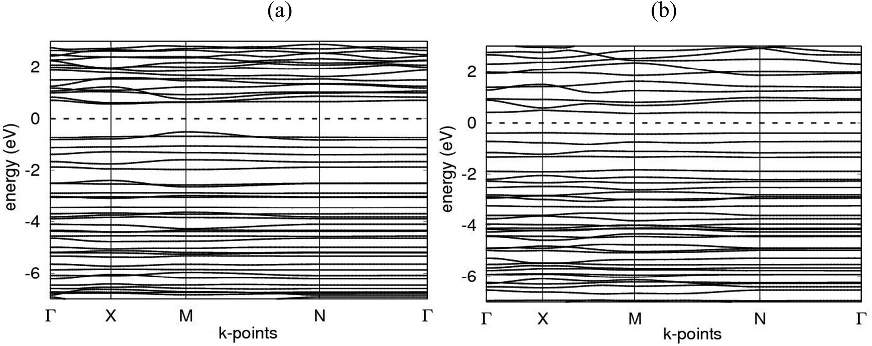 | ||
| Fig. 2 Computed band structures in the Γ–X–M–N–Γ direction for (a) nanoarchitecture-A, and (b) nanoarchitecture-B. The zero of the energy scale is set at the middle of the energy gap, Eg, between the valence and conduction bands. | ||
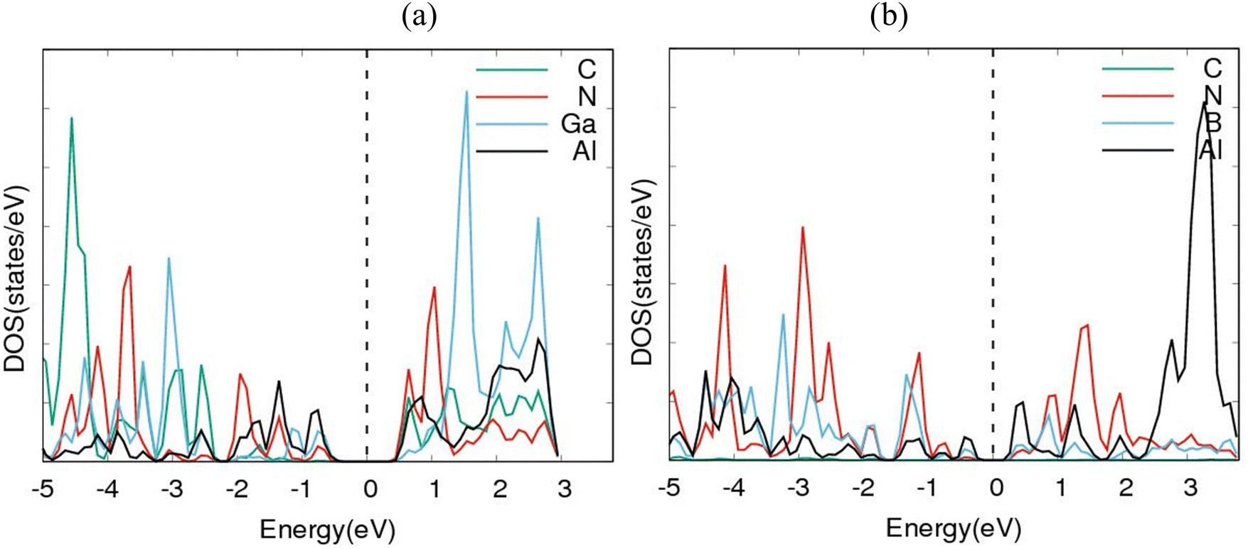
To further consolidate the results obtained and check the stability of the nanoheterostructures, the following calculations were carried out. The density of electronic states and projected density of electronic states for the nanoarchitecture-A and nanoarchitecture-B structures were plotted as depicted in Fig. 3(a), (b) and 4(a), (b), respectively. The total density of states (t-DOS) and partial density of states (p-DOS) are key electronic structure parameters useful in determining the different orbital overlapping (energy levels) in materials, and how their relaxation affects the arrangement of the different energy levels. The local state density and orbital projection states of AlN:CC:GaN:CC and AlN:CC:BN:CC designs are presented in Fig. 3(a), (b) and 4(a), (b) respectively. It can be seen that for the AlN:CC:GaN:CC structure, the conduction band contributions are due to 2p states of N and C atoms whilst for the valence band, the main contributions are from the 2p and 3p states of the Al and Ga atoms, respectively. In addition, covalence occurs between the 2p state of the Al atom and the 3p state of the Ga atom. Therefore, the AlN:CC:GaN:CC structure exhibits strong electronic sharing characteristics and excellent mobility within the layer, making it a promising semiconductor optoelectronic material. It can also be seen that the AlN:CC:BN:CC structure has a narrow bandgap energy band, the contribution of the conduction band mainly comes from the 2p states of Al and C atoms, and the contribution of the valence band mainly comes from the 1s state of Al and the 2p state of N. The positions of the CB and VB in the band structure diagrams were indispensable once CC doping with variable coverages of AlN, BN, and GaN occurred. The band gaps are located at the Ef. Fig. 4(a) and (b) depict only positive polarized electron spin states in all the structures. We have indicated in Fig. 5(a) and (b) a single plot for both DOS & TDOS to ascertain the exact role of the contributions of the orbital atoms to the density of electronic states.
 | ||
| Fig. 3 Electronic density of states (DOS) diagrams for (a) nanoarchitecture-A and (b) nanoarchitecture-B. | ||
 | ||
| Fig. 4 Partial density of states (p-DOS) diagrams for (a) AlN:CC:GaN:CC & (b) AlN:CC:BN:CC modes. | ||
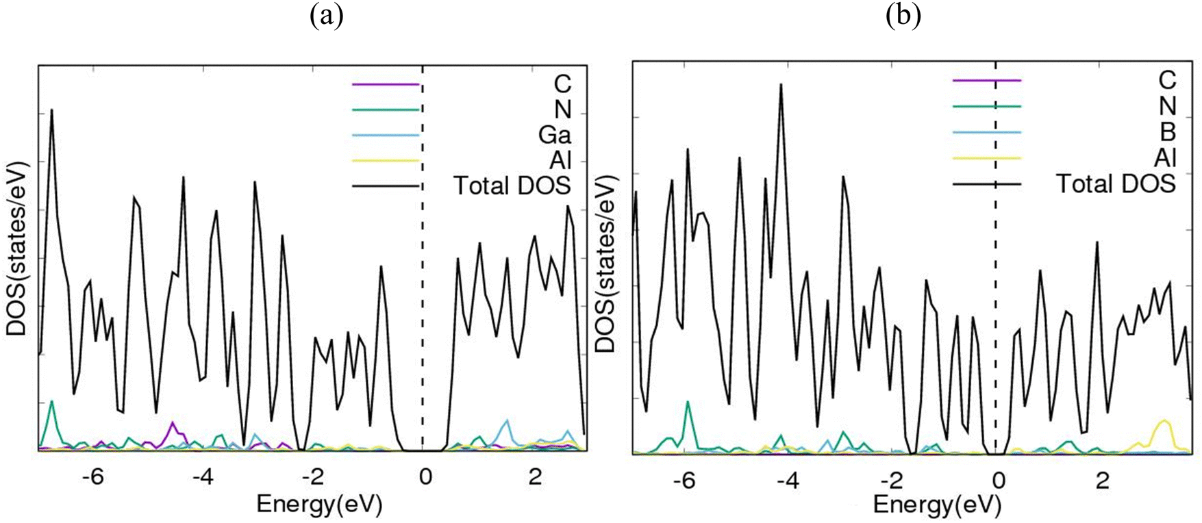 | ||
| Fig. 5 DOS & t-DOS plotted on the same axis for (a) AlN:CC:GaN:CC mode and (b) AlN:CC:BN:CC mode. EF designates Fermi energy level; the energy scale is set to zero. | ||
Comparing the band gaps among CC graphene, BN, AlN and the two new 2D nanoheterostructures, it is realized that new bands appeared due to hybridization processes. Band gap engineering and its applications rely heavily upon hybridized 2D nanoelements for nano-electronics and nano-optical devices.
3.4 Analysis of charge density
The charge density plots in Fig. 6(a) and (b) show a homogenous charge distribution among the nitrogen, carbon, boron, gallium and aluminium atoms, signifying that a significant chemical interaction took place. In terms of charge distribution, there is a uniform sharing among the nitrogen, carbon and boron atoms with respect to electronegativity values of 3.04, 2.55 and 2.04. There is also an excellent charge distribution between the gallium and aluminium atoms because of similar electronegativity values of 1.81 and 1.61 respectively. The PDOS plots in Fig. 4(a) and (b) indicate that the p-orbitals of carbon, boron, aluminium and nitrogen atoms all contributed significantly to the total density of states. The reason for this can be traced back to the charge density plots in Fig. 6(a) and (b). The plots show higher density of charges around the carbon and nitrogen atoms. This is apparently due to nitrogen having a comparable electronegativity value to that of carbon. As a result, the nitrogen and carbon atoms draw more electrons to themselves. Hence, a significant charge density cloud is observed around the nitrogen and carbon atoms in Fig. 6(a). In Fig. 6(b), a significant charge density cloud is observed around the carbon and boron atoms.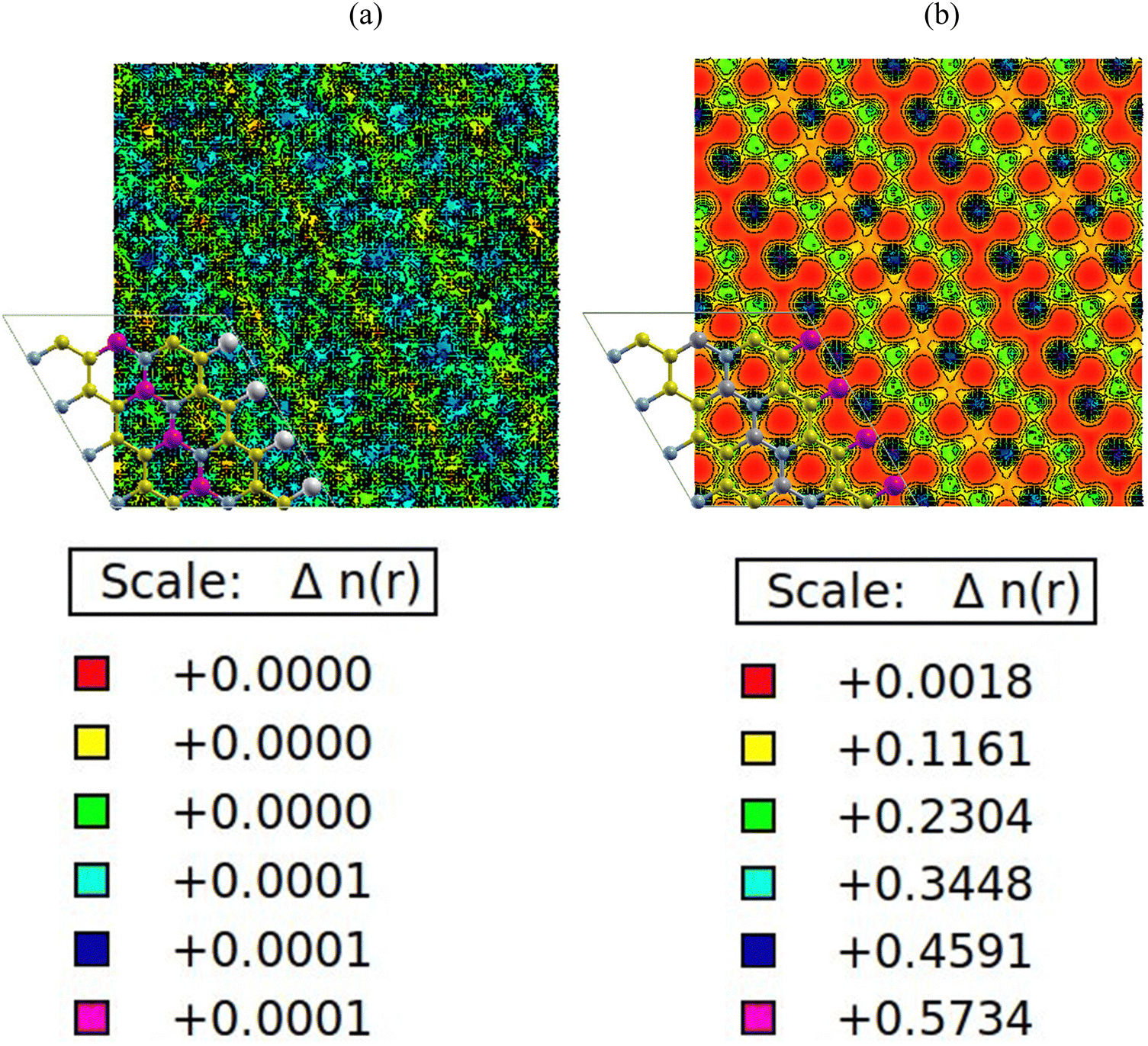 | ||
| Fig. 6 (a) AlN:CC:GaN:CC, (b) AlN:CC:BN:CC isoline–isosurface charge density. Violet depicts regions of maximum charge density. Red depicts regions of minimum density in charge. | ||
3.5 Optical absorption spectrum
The spectral absorption computations in AlN:CC:GaN:CC & AlN:CC:BN:CC are communicated by Fig. 7(a) and (b). They possess absorption in the visible and UV frequencies for parallel as well as perpendicular field directions. Using the GGA-PBE correlation–exchange functional, it was found that electronic excitations occurred in the ultraviolet (UV) spectral region, as shown in Fig. 7(a) and (b). From Fig. 7(a), it can be observed that the most intense absorption peaks occur in the UV region, in the approximate range 0.44–0.48 Ry, in the X-, Y- and Z-directions. In the region around 0.47–0.49 Ry, we found a change in the absorption curves, but with the X- and Y-directions absorbing more. We found that the nanoheterostructure absorbs most intensely in the ranges around 0.44 to 0.48 Ry and 0.47 to 0.50 Ry, and moderately near the region of 0.50 to 0.53 Ry. In the region below 0.4 Ry there is no loss of energy, as the absorption is zero, while in the region between approximately 0.49 and 0.55 Ry the energy loss becomes moderate and there is greater absorption in the X- and Y-directions. The first absorption peak occurs at approximately 0.46 Ry, a value that is compatible with the nanoheterostructure gap. In the energy region from 0.44 to 0.47 Ry, optical absorption is mainly due to electron transfer from the occupied Al 2p and C 2p orbitals to the virtual N 2p orbitals in the lower part of the conduction band. Peaks with energies of approximately 6–10 eV occur owing to electron transitions between the populated Al 2p states and the empty C 2p states. Similar analysis holds for Fig. 7(b). The fabricated 2D modes are observed to possess high anisotropy and stability. Based on the orientation and frequency dependent characteristics, they are capable of opening desired avenues for marvellous fabrications in electronics. They are observed to be the desired 2D nanomaterials possessing multiple properties and features. We believe that these new 2D structures are geared towards solutions to the world's search for optimum functionality in the fabrication quest because of the high direction-dependent nature.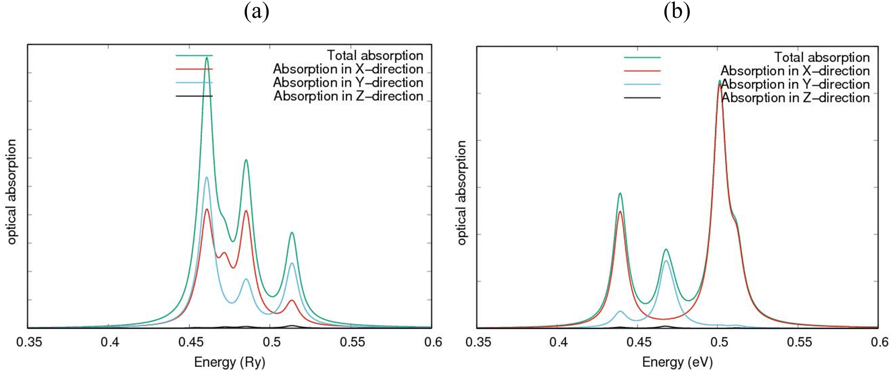 | ||
| Fig. 7 Computed optical absorption spectra for (a) AlN:CC:GaN:CC and (b) AlN:CC:BN:CC nanoheterostructures. | ||
3.6 Phonon dispersion analysis
The dispersion relations of the phonon calculations for AlN:CC:GaN:CC and AlN:CC:BN:CC nanoarchitectures in the Irreducible BZ are shown in Fig. 8(a) and (b). The dynamical matrices were computed along the high symmetry points Γ–N–M–K–X–L–N–Γ. The dynamical matrices at the BZ were obtained using the Fourier interpolation scheme. We observed an energy gap between the low-frequency and the high-frequency phonons which could be attributed to stretching originating from the symmetric and antisymmetric stretching modes in the supercells. The figure shows that the phonon dispersion curves for the nanoarchitectures in the whole Brillouin zone are positive (stable phonon modes) and in good agreement with the experimental data.49 The two highest phonon branches resulting from carbon atom vibrations are well separated from the other phonon branches. The upper branch of these two highest phonon branches is dispersionless or flat along the Γ–N, K–X and N–Γ directions, while the lower branches of these two highest phonon branches are dispersive. Below the gap region, all of the optical branches due to carbon atom vibrations are dispersive.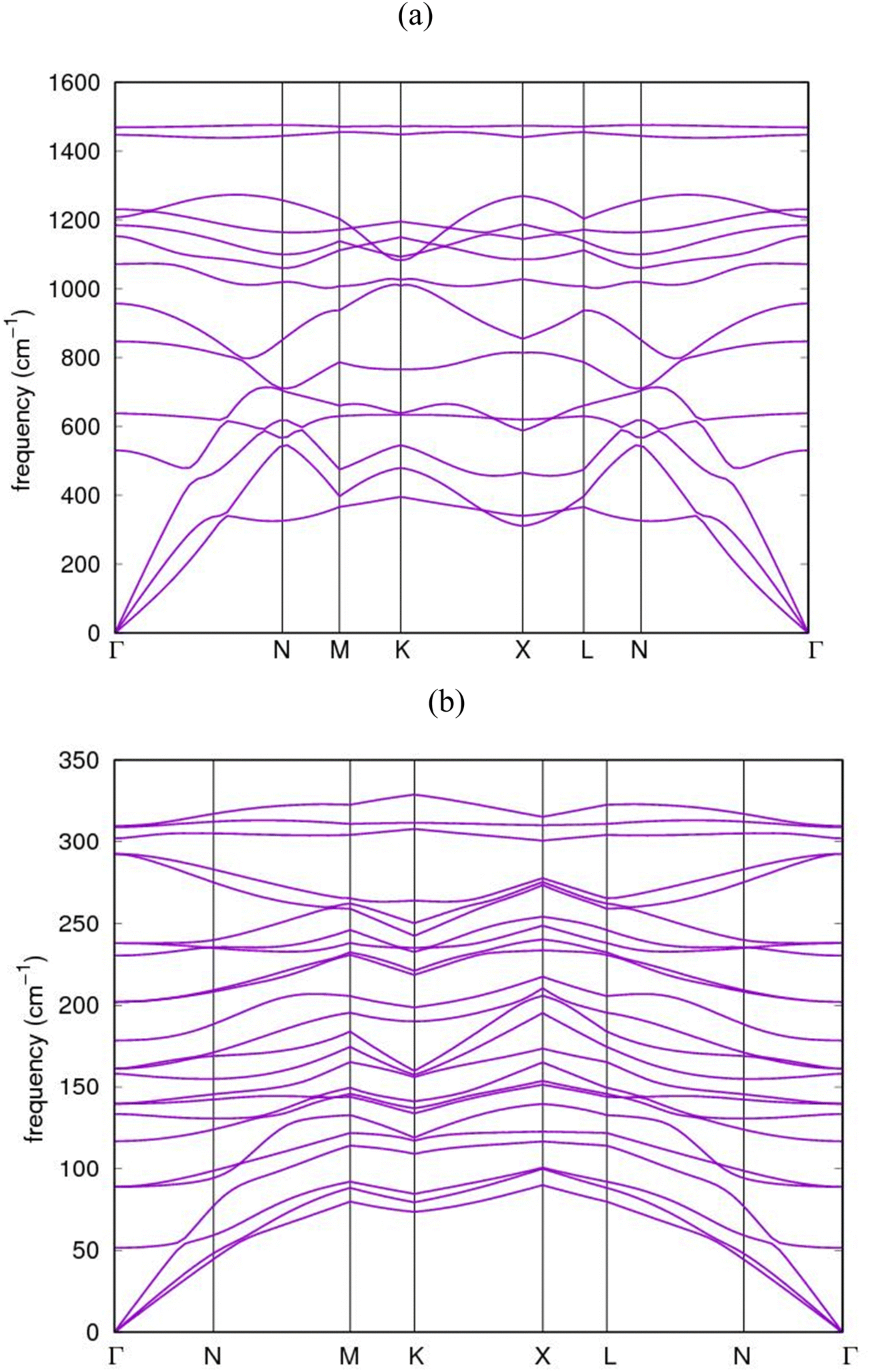 | ||
| Fig. 8 Calculated phonon dispersion band-structure for (a) AlN:CC:GaN:CC and (b) AlN:CC:BN:CC nanoheterostructures. | ||
The figures further show that the highest phonon branches are clearly separated from the lower branches without any degeneracy. A strong dispersive relation exists between the highest and the lowest branches. The transverse acoustic (TA) vibrations belong to the low-frequency modes whilst those of the longitudinal acoustic (LA) vibrations belong to the high-frequency modes and all the collective modes of vibrations originate from the C-atoms. Similarly, optical modes with higher frequencies are associated with the N-atom lattice vibrations. We observed again that, the AlN:CC:GaN:CC and AlN:CC:BN:CC phonon dispersions have their longitudinal optical (LO) and transverse optical (TO) modes splitting up at the Γ-point as a consequence of the long-range diploe order interaction usually associated with semiconductor and insulator polar materials.
Notwithstanding, the relatively large atomic mass difference between Ga and N atoms creates gaps, which is revealed in the region between the dominant acoustic and optical branch modes, respectively, because of the relative displacements between the atoms accordingly. The calculated dispersions for AlN:CC:GaN:CC and AlN:CC:BN:CC nanoarchitectures are in good agreement with the experimental observations.50 Nevertheless, our calculated phonon dispersion compares quite well with calculations of Isaev and colleagues51 and Heid's group.52
4. Conclusions
In this study, the structural, electronic, optical and vibrational properties of two new nanoheterostructure materials, AlN:CC:GaN:CC and AlN:CC:BN:CC, were calculated using DFT, DFPT and TDDFPT. The paper describes the application of density functional theory (DFT) methods in designing the two new 2D hybrid nanoheterostructures. Phonon dispersion computations revealed that the two new structures are thermodynamically stable. These nanoarchitectures are quantum-confined systems and therefore exhibit wide surface areas. The remarkable tunability of the optical properties in the 2D hybrid nanostructures and the possibility to modulate carrier mobility by changing the surface chemistry of the substrates are novel aspects of great practical interest. These materials have shown large optical absorption for visible and UV frequencies. From the optical properties profile, the polarizations along the in-plane and out-of-plane directions are different and therefore show anisotropic behaviours. Six prominent peaks were observed in the optical absorption spectrum of AlN:CC:GaN:CC. These materials may prove crucial for the development of devices with particular optical and electronic properties. The novel 2D nanoarchitectures can be used as highly promising materials in optoelectronics, ultraviolet optical nanodevices and photovoltaics.Author contributions
V. W. Elloh: conceptualization, investigation, methodology, formal analysis, writing – original draft. D. E. Anderson: methodology, resources, software, validation. D. Abbeyquaye: visualization, data curation, formal analysis, writing – review & editing. D. F. Ofosuhene: visualization, software, data curation. I. Arhin: visualization, software, writing – review & editing. E. Okoampa Boadu: visualization, resources, validation. A. Yaya: supervision, project administration, funding acquisition. Eric K. K. Abavare: visualization, project administration, supervision.Data availability
The DFT data used to support the findings of this study are included within the article.Conflicts of interest
The authors declare that they have no known competing financial interests or personal relationships that could have appeared to influence the work reported in this paper.Acknowledgements
This research received no external funding. The authors are very grateful to the Centre for High-Performance Computing (CHPC), Cape Town, South Africa, for computer time on the Lengau cluster.References
- Y. Zhu, S. Murali, W. Cai, X. Li, J. W. Suk, J. R. Potts and R. S. Ruoff, Adv. Mater., 2010, 22, 3906 CrossRef CAS PubMed.
- F. Schwierz, Nat. Nanotechnol., 2010, 5, 487 CrossRef CAS PubMed.
- F. Bonaccorso, Z. Sun, T. Hasan and A. C. Ferrari, Nat. Photonics, 2010, 4, 611 CrossRef CAS.
- M. D. Stoller, S. J. Park, Y. W. Zhu, J. H. An and R. S. Ruoff, Nano Lett., 2008, 8, 3498 CrossRef CAS PubMed.
- X. L. Li, X. R. Wang, L. Zhang, S. W. Lee and H. J. Dai, Science, 2008, 319, 1229 CrossRef CAS PubMed.
- A. K. Geim and K. S. Novoselov, Nat. Mater., 2007, 6, 183 CrossRef CAS PubMed.
- K. S. Novoselov, A. K. Geim, S. V. Morozov, D. Jiang, Y. Zhang, S. V. Dubonos, I. V. Grigorieva and A. A. Firsov, Science, 2004, 306, 666 CrossRef CAS.
- S. L. Zhang, Y. H. Hu, Z. Y. Hu, B. Cai and H. B. Zeng, Appl. Phys. Lett., 2015, 107, 022102 CrossRef.
- B. Cai, S. L. Zhang, Z. Y. Hu, Y. H. Hu, Y. S. Zou and H. B. Zeng, Phys. Chem. Chem. Phys., 2015, 17, 12634 RSC.
- D. Jose and A. Datta, Acc. Chem. Res., 2014, 47, 593 CrossRef CAS PubMed.
- E. Bianco, S. Butler, S. S. Jiang, O. D. Restrepo, W. Windl and J. E. Goldberger, ACS Nano, 2013, 7, 4414 CrossRef CAS.
- M. P. Levendorf, C. J. Kim, L. Brown, P. Y. Huang, R. W. Havener, D. A. Muller and J. Park, Nature, 2012, 488, 627 CrossRef CAS PubMed.
- M. Houssa, E. Scalise, K. Sankaran, G. Pourtois, V. V. Afanas’ev and A. Stesmans, Appl. Phys. Lett., 2011, 98, 223107 CrossRef.
- S. Das Sarma, S. Adam, E. H. Hwang and E. Rossi, Rev. Mod. Phys., 2011, 83, 407 CrossRef CAS.
- K. F. Mak, C. Lee, J. Hone, J. Shan and T. F. Heinz, Phys. Rev. Lett., 2010, 105, 136805 CrossRef.
- A. H. Castro Neto, F. Guinea, N. M. R. Peres, K. S. Novoselov and A. K. Geim, Rev. Mod. Phys., 2009, 81, 109 CrossRef CAS.
- A. Gupta, T. Sakthivel and S. Seal, Prog. Mater. Sci., 2015, 73, 44 CrossRef CAS.
- Q. H. Wang, K. Kalantar-Zadeh, A. Kis, J. N. Coleman and M. S. Strano, Nat. Nanotechnol., 2012, 7, 699 CrossRef CAS PubMed.
- F. Xia, H. Wang, D. Xiao, M. Dubey and A. Rama Subramaniam, Nat. Photonics, 2014, 8, 899 CrossRef CAS.
- F. Yang, S. Cheng, X. Zhang, X. Ren, R. Li, H. Dong and W. Hu, Adv. Mater., 2018, 30, 1702415 CrossRef.
- V. W. Elloh, E. O. Boadu, G. Gebreyesus, A. K. Mishra, D. Dodoo-Arhin and A. Yaya, Hybrid Adv., 2023, 3, 100045 CrossRef.
- K. S. Novoselov, Proc. Natl. Acad. Sci. U. S. A., 2005, 102, 10451 CrossRef CAS PubMed.
- A. K. Geim and I. V. Grigorieva, Nature, 2013, 499, 419 CrossRef CAS PubMed.
- G. R. Bhimanapati, ACS Nano, 2015, 9, 11509 CrossRef CAS PubMed.
- T. Tan, X. Jiang, C. Wang, B. Yao and H. Zhang, Adv. Sci., 2020, 7, 2000058 CrossRef CAS.
- S. Kang, 2D Mater., 2020, 7, 022003 CrossRef CAS.
- M. Bernardi, C. Ataca, M. Palummo and J. Grossman, Nanophotonics, 2016, 6, 479 Search PubMed.
- V. W. Elloh, A. Yaya and E. K. K. Abavare, Next Mater., 2024, 5, 100224 CrossRef.
- F. A. Rasmussen and K. S. Thygesen, J. Phys. Chem. C, 2015, 119, 13169 CrossRef CAS.
- S. Manzeli, D. Ovchinnikov, D. Pasquier, O. V. Yazyev and A. Kis, Nat. Rev. Mater., 2017, 2, 17033 CrossRef CAS.
- N. K. Nassiri, Nat. Commun., 2021, 12, 7034 CrossRef.
- L. Bastonero, G. Cicero, M. Palummo and M. R. Fiorentin, ACS Appl. Mater. Interfaces, 2021, 13, 43615 CrossRef CAS PubMed.
- J. Zha, Adv. Funct. Mater., 2022, 32, 2111970 CrossRef CAS.
- A. Taffelli, S. Diré, A. Quaranta and L. Pancheri, Sensors, 2021, 21, 2758 CrossRef CAS PubMed.
- C. Wang, F. Yang and Y. Gao, Nanoscale Adv., 2020, 2, 4323 RSC.
- T. Mueller and E. Malic, 2D Mater. Appl., 2018, 2, 29 CrossRef.
- C. Robert, Nat. Commun., 2020, 11, 4037 CrossRef CAS PubMed.
- E. Malic, Phys. Rev. Mater., 2018, 2, 014002 CrossRef CAS.
- P. Giannozzi, J. Phys.: Condens. Matter, 2009, 21, 395502 CrossRef PubMed.
- J. P. Perdew, K. Burke and Y. Wang, Phys. Rev. B: Condens. Matter Mater. Phys., 1996, 54, 16533 CrossRef CAS PubMed.
- A. M. K. Rappe, M. Rabe, E. Kaxiras and J. D. Joannopoulos, Phys. Rev. B: Condens. Matter Mater. Phys., 1990, 41, 1227 CrossRef PubMed.
- S. Grimme, J. Comput. Chem., 2006, 27, 1787 CrossRef CAS PubMed.
- S. Grimme, J. Antony, S. Ehrlich and H. Krieg, J. Chem. Phys., 2010, 132, 154104 CrossRef.
- Q. Guo, K. C. Lau and R. Pandey, Mater. Adv., 2021, 2, 6403 RSC.
- Q. Guo, K. C. Lau and R. Pandey, J. Phys. Chem. C, 2019, 123, 4674 CrossRef CAS.
- H. J. Monkhorst and J. D. Pack, Phys. Rev. B: Solid State, 1976, 13, 5188 CrossRef.
- T. Bjorkman and O. Granas, Int. J. Quantum Chem., 2011, 111, 1025 CrossRef.
- S. Baroni, S. de Gironcoli, A. D. Corso and P. Giannozzi, Rev. Mod. Phys., 2001, 73, 515 CrossRef CAS.
- M. Baibarac, I. S. Baltog, P. Lefrant and G. Romero, Polymer, 2007, 48, 5279 CrossRef CAS.
- S. Duman, S. Bagci, H. M. Tutuncu, G. Ugur and G. P. Srivastava, Diamond Relat. Mater., 2006, 15, 1175 CrossRef CAS.
- E. I. Isaev, S. I. Simak, I. A. Abrikosov, R. Ahuja, Y. K. Vekilov, M. I. Katsnelson, A. I. Lichtenstein and B. Johansson, J. Appl. Phys., 2007, 101, 123519 CrossRef.
- R. Heid, K. P. Bohnen, B. Renker, T. Wolf and H. Schober, Phys. Rev. B: Condens. Matter Mater. Phys., 2005, 71, 092302 CrossRef.
| This journal is © The Royal Society of Chemistry 2024 |