
 Open Access Article
 This Open Access Article is licensed under a Creative Commons Attribution-Non Commercial 3.0 Unported Licence
Dual-functionality of CZTS nanoflakes: as an anode material for lithium-ion batteries and as a counter electrode in DSSCs – a DFT and experimental investigation†
G.
Rajesh‡
 *ab,
Jeyakiruba
Palraj‡
c,
Venkatraman
M. R.
d,
Ramesh
Sivasamy
e,
Sreejith P.
Madhusudanan
f,
Helen Annal
Therese
c and
Marcos
Flores
b
*ab,
Jeyakiruba
Palraj‡
c,
Venkatraman
M. R.
d,
Ramesh
Sivasamy
e,
Sreejith P.
Madhusudanan
f,
Helen Annal
Therese
c and
Marcos
Flores
b
aCenter for Research in Pure and Applied Science (CRPAS), JAIN Deemed to be university, Bengaluru, India. E-mail: rajesh.govind88@gmail.com
bLaboratory of Surfaces and Nanomaterials, Physics Department, FCFM, Universidad de Chile, Santiago, Chile
cDepartment of Chemistry, Faculty of Engineering and Technology, SRM Institute of Science and Technology, Kattankulathur Campus, Chennai, India
dCentre for Computational Modelling, Chennai Institute of Technology, Chennai, India
eAcademic centre for Materials and Nanotechnology (ACMIN), AGH University of Science and Technology, Krakow, Poland
fDepartment of Civil Engineering, Indian Institute of Technology Palakkad, Kanjikode, Kerala, India
First published on 18th June 2024
Abstract
This research work aims to develop a new dual-functional electrode material suitable for both lithium-ion batteries (LIBs) and dye-sensitized solar cells (DSSCs). Nanostructured Cu2ZnSnS4 (CZTS) was synthesized through the solvothermal method. Structural properties analysed through the X-ray diffraction pattern (XRD) and Raman spectra reveal the formation of the CZTS with kesterite structure . The stoichiometry and the oxidation states of CZTS have been analyzed using X-ray photoelectron spectroscopy (XPS). The core level XPS spectra of Cu 2p, Zn 2p, Sn 3d, and S 2p confirm the presence of the constituent elements in the required oxidation states (Cu+, Zn2+, Sn4+, S2−). The surface morphology of the CZTS nanoparticles showed a nanoflake-like structure with a surface area of 34.20 m2 g−1. The geometrical optimization, electronic, and optical properties were calculated using DFT calculations. The semiconducting material CZTS is electrochemically active toward Li, which can be used as an alternative anode material for lithium-ion batteries offering potential improvements in cycling stability and specific capacity. The electrochemical studies of the CZTS nanoflakes exhibited a specific capacity of 1141.08 mA h g−1 and 350 mA h g−1 at 0.1C and 1C rates respectively. The cycling stability of CZTS at a high scan rate of 1C, and the specific capacity of 220 mA h g−1 over 70 cycles with 73% coulombic efficiency, suggest it to be a promising alternative anode material in the next-generation lithium-ion batteries. The performance of CZTS as a counter electrode in dye-sensitized solar cells was also explored. The DSSC constructed with CZTS as the counter electrode showed an efficiency of 5.9%.
Introduction
Technological advancements today have increased the need for energy-efficient and smart materials with multiple utilities.1 On the other hand, rapidly expanding CO2 discharges and dependence on non-renewable energy source assets have become worldwide energy concerns. Technologies to meet the energy requirements of the modern world with negligible pollution to the environment remain the top priority of research today. Among the different technologies, solar cells, lithium-ion battery technologies and electrochemical supercapacitors2,3 have emerged as the most promising choices for energy harvesting and storage. Compared to traditional lead-acid batteries, lithium-ion batteries have significant advantages in terms of cycle life, power and energy density, efficiency design, flexibility, and large-scale applications.4–8The lithium-ion battery energy storage and supply mechanism involves inserting and extracting lithium ions within the electrode materials during charge and discharge cycles. The performance of the battery is primarily determined by its energy and power densities. To enhance these properties and cycle life, careful selection of electrode materials and electrolytes is essential. Cathode materials store energy through intercalation or conversion reactions, while anode materials engage in intercalation, conversion reactions, or alloying/dealloying for energy storage. Depending on the specific electrode material, one or more of these mechanisms can occur, directly impacting the battery's overall performance.9,10 Thus, the characteristics of the anode material play a crucial role in determining the electrochemical performance of lithium-ion batteries.
Graphite has been widely used as a primary anode material in commercial lithium-ion batteries owing to its advantageous characteristics such as conductivity, good reversibility, and relatively low cost. However, its energy density is limited because the six carbon atoms can only accommodate one lithium atom. Silicon has emerged as a promising alternative with approximately ten times more capacity than graphite.11–13 However, the significant volume expansion of silicon during lithium insertion and extraction leads to issues such as pulverization, the formation of an unstable solid–electrolyte interphase (SEI), and the loss of electrical contact, resulting in capacity degradation and limited cycle life.14
Extensive research efforts have focused on finding alternative materials that can offer superior energy capacity and cycling stability compared to graphite and silicon.15 Tin-based lithium storage materials, known for their high theoretical capacity, have emerged as a promising substitute for graphite in the next generation of lithium-ion batteries.16 Among these materials, tin-sulfide stands out with its superior cycling stability and significantly larger reversible capacities, making it one of the most prospective candidates for high-performance anode materials in lithium-ion batteries.17–21 However, the long-term stability of tin-sulfide materials and their suitability within specific voltage ranges have not met the desired standards. To enhance the capacity characteristics of tin-based anodes without compromising energy density, numerous strategies have been investigated. One such strategy involves designing nanostructured electrode materials with significant advantages,16 including a short diffusion path of lithium ions, easy penetration of electrolytes, and highly available charge storage sites due to the high surface area. An alternative approach involves creating composite structures by combining tin-based materials with conducting materials, introducing elements such as (Cu, Zn, S) into Sn-based materials, improving the electrical conductivity, and serving as a buffer matrix during Li insertion.22,23 Other materials such as porous TiO2 wires,24 microspheres,25 and porous MnO2/C nanospheres26 have also been utilized as anode materials in Li-ion batteries.
Various researchers have used different methods to synthesize nanostructured CZTS; Zhou et al.23 synthesized flower-like Cu2ZnSnS4 nanostructures via a solvothermal technique, demonstrating stable lithium-ion reversibility, but with a lithium storage capacity of 150 mA h g−1. Li et al.17 synthesized kesterite Cu2ZnSnS4 nanocrystals using a cost-effective wet chemical process, achieving an initial 540 mA h g−1 discharge capacity. Meanwhile, Yang et al.27 synthesized CZTS nanocrystals with a microwave-assisted approach, but with a reversible capacity of 288 mA h g−1. Therefore, a reasonable design of electrode materials with cycling ability and high-rate performance is needed.
Exploring a variety of applications of the materials is essential as it will be useful in the future for the large-scale production of similar materials for various applications. Dye-sensitized solar cells (DSSC), which fall under the group of third-generation solar cells, have attracted interest for their variety of advantages, such as their capacity to work under diffused light conditions, and lightweight and semi-transparent nature, which makes them an attractive candidate for window applications.28 In DSSCs, mesoporous TiO2 sensitized with a dye forms the photoanode layer,29 and a thin layer of platinum coated over conducting substrates has been used as the counter electrode. However, to reduce the manufacturing cost towards commercialization, various other counter electrode materials have also been tested. Among them, CZTS has also been reported as an efficient counter electrode material, and it also has the unique edge of being made of earth-abundant material that can be relatively cheaper than platinum-based counter electrodes.30,31
In the present work, we developed nanostructured Cu2ZnSnS4 (CZTS) for dual applications, as an alternative anode material for lithium-ion batteries and as a counter electrode in DSSCs, by taking advantage of our earlier experience in the fabrication of widely recognized CZTS solar cell absorber materials in thin film solar cells (TFSCs).27 In this study, kesterite CZTS nanoflakes were synthesized through a simple solvothermal method, without using expensive vacuum techniques.
Experimental
(a) Synthesis of the kesterite CZTS
All the chemicals employed in this study were of analytical reagent (AR) grade and used without additional purification. Cu2ZnSnS4 nanoparticles were synthesized via the solvothermal method without using catalysts, capping agents, or surfactants. To achieve this, stoichiometric amounts of (Cu (NO3)2), (Zn (NO3)2), (SnCl4), and thiourea were dissolved in a mixture of 2-methoxy ethanol and ethanolamine at room temperature. The resultant solution was stirred for 45 minutes using a magnetic stirrer, producing a homogeneous, clear, and transparent solution. Subsequently, the solution was transferred into an autoclave and maintained at 90 °C for 12 hours. Afterward, the resulting precipitates were centrifugated at 5000 rpm for 10 minutes, followed by several rinses with deionized water. The precipitates were dried at 70 °C for 24 hours and then annealed at 200 °C for 1 hour.(b) Characterization
The sample's structure and crystallinity were assessed using an X-ray diffractometer (Bruker D8 Advance) equipped with a Cu Kα radiation source (λ = 0.15406 nm) operating at a voltage of 40 kV and a current of 40 mA. A Renishaw instrument with a wavelength of 514.5 nm was employed to analyze the Raman spectrum. A field electron scanning electron microscope (CARL ZEISS-SIGMA) was used to examine the CZTS nanoparticles for surface morphology analysis. The microstructural properties of the CZTS nanoparticles were investigated using a high-resolution transmission electron microscope (HRTEM) with the JEOL JEM-ARM200F instrument. For the characterization of the surface and chemical states, X-ray photoelectron spectroscopy (XPS) was employed, using the Omicron ESCA system manufactured by Oxford Instruments Germany, which is a powerful technique for surface analysis providing elemental information and chemical state analysis (electron spectroscopy for chemical analysis (ESCA)). The surface area and pore size distribution of the CZTS nanoparticles have been investigated using the Quanta chrome Novae 2200 instrument. I–V measurements for the fabricated cells were carried out using a Keithley 2450 source meter under the illumination of 1 Sun with an ORIEL Solar Simulator under standard conditions. Incident photo to current conversion efficient (IPCE) curves of the DSSCs were performed using a system consisting of a Xe lamp (300 W) with an Oriel Newport Corp., monochromator.(c) Electrochemical measurements
CR2032 coin-type cells were employed in an automatic battery tester system (Bio-logic SAS, France) for charge-/discharge studies. The working electrode was prepared by a mixture of 70 wt% as-prepared powders (active material), 20 wt% carbon black, and 10 wt% poly (vinylidene fluoride) (PVDF) binder and NMP (N-methyl pyrrolidone) used as a solvent to make a slurry. The homogeneous slurry was coated on the copper foil and dried at 70 °C overnight in a vacuum oven. Lithium chips served as the counter electrode, and the electrolyte was 1 M LiPF6 dissolved in a mixture of ethylene carbonate (EC) and dimethyl carbonate (DEC) in a 1![[thin space (1/6-em)]](https://www.rsc.org/images/entities/char_2009.gif) :1 ratio (v/v). All test cells were assembled inside an argon-filled glove box with oxygen and moisture levels below 1 ppm each to maintain an oxygen and moisture-free environment. The cells underwent discharge and charge cycles at a rate of 0.1C, covering a voltage range of 0.01–3.00 V (vs. Li+/Li) at room temperature. The typical masses of electrode materials used in the experiments ranged from 2 to 3 mg. Cyclic voltammetry was also conducted using the Bio-logic SAS system within the voltage range of 0 and 3.0 V (vs. Li/Li+) at a scan rate of 0.5 mV s−1 at room temperature.
:1 ratio (v/v). All test cells were assembled inside an argon-filled glove box with oxygen and moisture levels below 1 ppm each to maintain an oxygen and moisture-free environment. The cells underwent discharge and charge cycles at a rate of 0.1C, covering a voltage range of 0.01–3.00 V (vs. Li+/Li) at room temperature. The typical masses of electrode materials used in the experiments ranged from 2 to 3 mg. Cyclic voltammetry was also conducted using the Bio-logic SAS system within the voltage range of 0 and 3.0 V (vs. Li/Li+) at a scan rate of 0.5 mV s−1 at room temperature.
(d) Computational studies
The CZTS DFT studies of the structural optimization, electronic structure, and optical properties of the materials were obtained using DFT calculation. The GGA-PBE function was employed in electronic structure computations. All the calculations were carried out using the periodic boundary conditions. A 3 × 3 × 2 Monkhorst–Pack (MP) grid was applied for Brillouin zone integration, and the cutoff energy was set to 498 eV. Specific criteria were determined to attain geometric convergence, including maximum force, most significant shift, maximum stress, and most remarkable energy alteration, which were assigned values of 1.0 × 10⁻⁵, 0.03 eV Å−1, 0.05 GPa, and 0.001 Å, correspondingly.Results and discussion
(a) Structural study
The structural properties of the CZTS nanoparticles have been studied using the X-ray diffraction technique. The X-ray diffraction pattern of the CZTS nanoparticles annealed at 200 °C is compared with their simulated pattern, as shown in Fig. 1. All the predominant peaks of the experimental pattern are comparable to the simulated pattern. The diffraction peaks observed at the 2θ positions of 28.3, 33.6, 47.3 and 55.2 were indexed to the (112), (200), (220) and (312) planes of CZTS with the tetragonal kesterite structure of Cu2ZnSnS4 (JCPDS, card no. 26-0575). Additionally, to comprehend the crystal structure, the Rietveld refinement analysis was executed to obtain full structural parameters. The refinement results of the synthesized sample show the I![[4 with combining macron]](https://www.rsc.org/images/entities/char_0034_0304.gif) 2m (121) space group. In the refined structure, the 4d Wyckoff position is particularly occupied by Zn and Cu, the 2a is engaged by Cu, the 2b position by Sn, and the 8i position is occupied by S. The calculated lattice parameters a, b, and c, and cell volume (V) are 5.43, 5.43, 10.80, and 318.8, respectively. Refined crystal structure data and the structure are shown in the ESI,† S1 and Table ST1, respectively. In the kesterite structure S1, each sulfur anion forms bonds with four cations, and each cation is bonded to four sulfur anions. The crystallographic c-direction exhibits alternating layers of cations (CuZn/SS/CuSn/SS) and sulfur anions.32
2m (121) space group. In the refined structure, the 4d Wyckoff position is particularly occupied by Zn and Cu, the 2a is engaged by Cu, the 2b position by Sn, and the 8i position is occupied by S. The calculated lattice parameters a, b, and c, and cell volume (V) are 5.43, 5.43, 10.80, and 318.8, respectively. Refined crystal structure data and the structure are shown in the ESI,† S1 and Table ST1, respectively. In the kesterite structure S1, each sulfur anion forms bonds with four cations, and each cation is bonded to four sulfur anions. The crystallographic c-direction exhibits alternating layers of cations (CuZn/SS/CuSn/SS) and sulfur anions.32
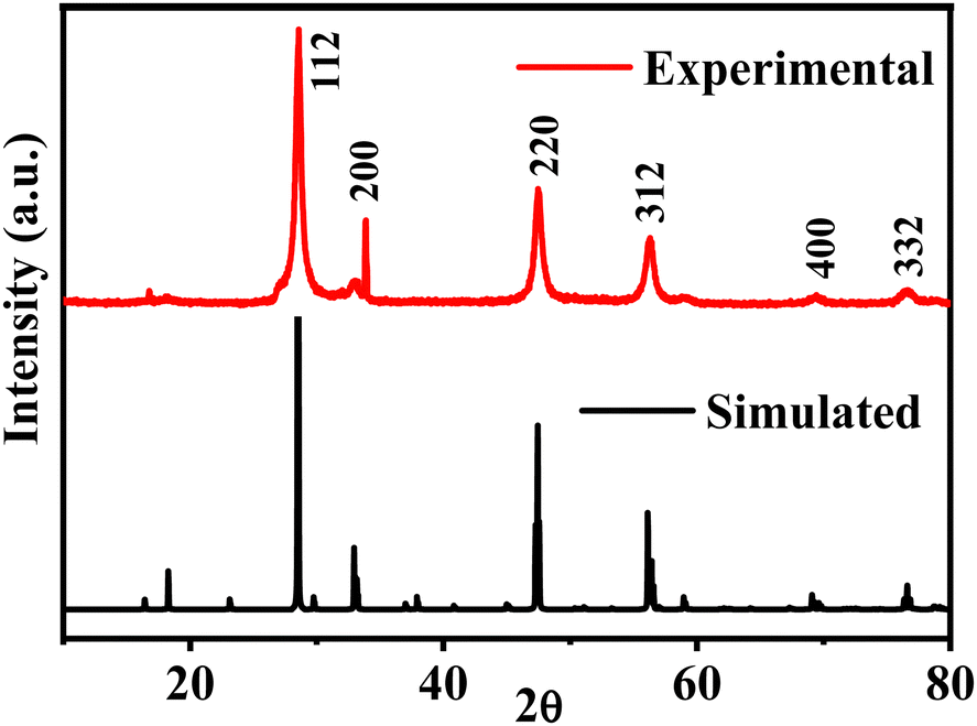 | ||
| Fig. 1 A comparison of the X-ray diffraction pattern of the experimental CZTS nanoparticles with the corresponding simulated pattern. | ||
As a quaternary compound, CZTS often contains various binary and ternary phases, making it challenging to control its stoichiometry precisely. The lack of sulfur during the formation of CZTS leads to several secondary phases, including ZnS, CuS, Sn2S3, SnS2, and Cu2SnS3. These secondary phases have crystal structures similar to CZTS, resulting in overlapping peaks in the X-ray diffractogram, making it difficult to distinguish CZTS from the secondary phases. Moreover, numerous reports indicate that CZTS tends to lose its anion (sulfur) during the annealing process due to the high volatility of sulfur. Consequently, when CZTS is annealed without a sulfur atmosphere, it exhibits the presence of secondary phases.33 Raman spectroscopy provides a more reliable indication of the presence of secondary phases in CZTS, as each phase in CZTS exhibits distinct peak positions in Raman scattering which is more distinct than in the X-ray diffraction pattern. The Raman spectrum of CZTS nanoparticles is shown in Fig. 2. The vibration frequency at 331 cm−1 confirms the formation of kesterite CZTS. The strong peak position at 331 cm−1 corresponds to the A1 mode of CZTS. The A1 modes in CZTS nanoparticles represent pure anion vibrations, specifically involving sulfur atoms surrounded by neighbouring atoms that remain motionless.34 The broadening of these modes indicates the phonon confinement effects within the nanoparticles.
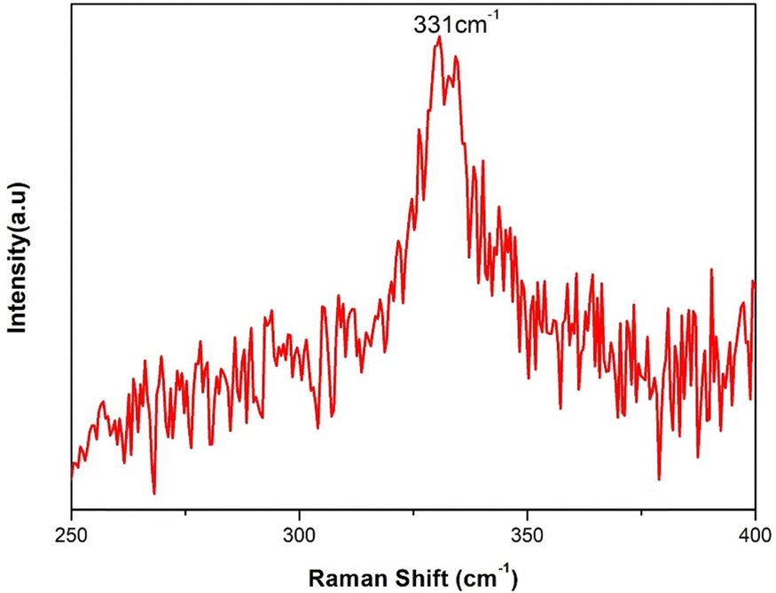 | ||
| Fig. 2 Raman spectrum of kesterite phase CZTS nanoparticles. | ||
(b) Morphological and compositional study
Fig. 3(a) shows the surface morphology of the CZTS nanoparticles via the field emission scanning electron microscope (FESEM) images. The FESEM image reveals the formation of CZTS nanoflake-like structures. It can be seen that the CZTS nanoflakes are composed of dense and homogeneous structures that are uniform in nature.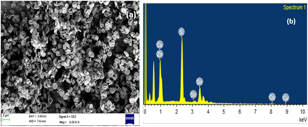 | ||
| Fig. 3 (a) FESEM image of CZTS (Cu2ZnSnS4) nanoparticles and (b) EDAX spectrum of CZTS nanoparticles. | ||
Also, the energy dispersive X-ray analysis (EDAX) has been used to study the elemental composition of the CZTS nanoparticles. The EDAX spectra of the synthesized CZTS nanoparticles are shown in Fig. 3(b). EDAX analysis reveals that the constituent elements Cu, Zn, Sn, and S of CZTS are present in the sample, and it shows the formation of CZTS with almost stoichiometric composition. The chemical composition of the CZTS particles was found to be Cu 22.4 at%, Zn 12.2 at%, Sn 15.8 at%, and S 49.6 at%, respectively, within the nanoparticles.
High resolution (TEM) has been used to analyze the microstructure of the CZTS nanoparticles. For high-resolution transmission electron microscopy analysis, the prepared CZTS nanoparticles were dispersed in acetone, and the solution was sonicated for 10 minutes.
The high-resolution transmission electron microscope (HRTEM) images of the CZTS nanoparticles annealed at 200 °C are shown in Fig. 4. The HRTEM image shows the lattice fringes, indicating the formation of nanocrystalline CZTS nanoparticles. The HRTEM image exhibits lattice fringes with a d spacing of 3.10 Å corresponding to the (112) reflection of the kesterite CZTS.
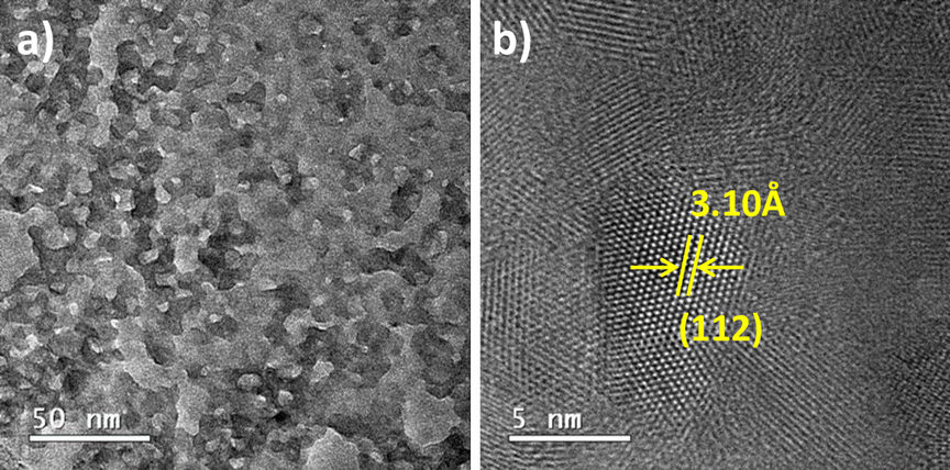 | ||
| Fig. 4 (a) and (b) High-resolution transmission electron microscope images of CZTS nanoparticles. | ||
(c) Surface study
X-ray photoelectron spectroscopy (XPS), a surface-sensitive technique, was utilized to examine the stoichiometry and oxidation states of the constituent elements in the CZTS nanoparticles. Fig. 5 shows the core level spectra of Cu 2p, Zn 2p, Sn 3d, and S 2p obtained from the XPS analysis. The peak of Cu 2p is split into two peaks (Fig. 5b) and is observed at 932.1 eV (2p3/2) and 951.9 eV (2p1/2) with a splitting energy of 19.8 eV, indicating the formation of Cu+. The 2p peak of Zn (Fig. 5a) was observed at the binding energies of 1022.01 (2p3/2) and 1044.9 eV (2p1/2) with a splitting energy of 22.9 eV corresponding to Zn(II). This peak separation was due to the formation of Zn2+. The peak of Sn 3d (Fig. 5 c) split into 486.3 (2p5/2) and 494.7 eV (2p3/2) with a splitting energy of 8.4 eV, and this is attributed to Sn(IV) due to the so-called final state effects. The 2p peak of S (Fig. 5d) was located at 161.35 eV and 162.55 eV with splitting energy of 1.20 eV, which is consistent with the 160–164 eV range expected for S in sulfide phases,35 which also indicates that sulfur is present in the S2− state.36 The S 2p spectra show the region which belongs to sulfur emission. The peaks fitted at 161.35 and 162.55 are assigned to S 2p3/2 and S 2p1/2 respectively, which indicates that the sulfur is in the S2− oxidation state.36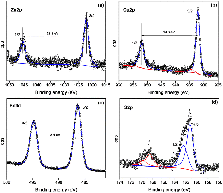 | ||
| Fig. 5 X-ray photoelectron spectra of (a) Zn 2p, (b) Cu 2p, (c) Sn 3d, (d) S 2p of CZTS nanoparticles. | ||
The textural properties, such as surface area and the total pore volume of the CZTS nanoparticles, were evaluated based on N2 adsorption–desorption isotherms shown in Fig. 6. The inset depicts the pore size distribution of CZTS nanoparticles. Based on the Brunauer–Deming–Deming Teller (BDDT) classification, physisorption isotherms can be categorized into six types, and the hysteresis loop shapes are used to determine the specific pore structure. CZTS nanoparticles correspond to type-IV isotherms and type-H3 hysteresis loops. The observed BET surface area of CZTS is 34.20 m2 g−1. The Barrett–Joyner–Halenda (BJH) pore size distribution curve (inset) indicates the high degree of uniformity of the pores in the range of 3.3 nm for CZTS.
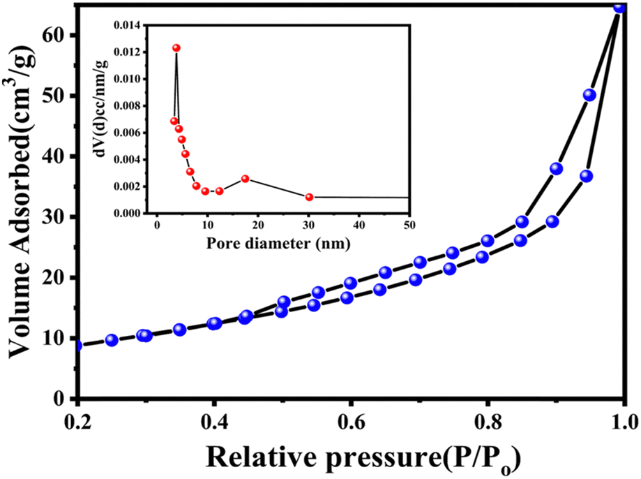 | ||
| Fig. 6 BET surface area analysis of a Cu2ZnSnS4 nanoparticle. The inset depicts the Barrett–Joyner–Halenda pore size distribution curves. | ||
(d) DFT study
We executed the structural optimization, electronic structure, and optical property simulations through DFT calculations employing the Cambridge Serial Total Energy Package (CASTEP) code. After the structural optimization, we executed electronic structure calculations to obtain the density of states and band structure. Fig. 7 and Fig. S2 (ESI†) correspondingly exhibit the band structure and the site-projected partial density of states (PDOS). A dotted line in the electronic structures is denoted as the Fermi level. According to the band structure, the valence band maximum (VBM) and the conduction band minimum (CBM) appear near the G-position with a 0.5 eV narrow bandgap of 0.5 eV. This value is underestimated compared to reported structures because of the use of the GGA-PBE functional owing to computational constraints. However, the features and impact of the band and density of states remain comparable to those found using the HSE functional, offering a valuable understanding of the material properties. From the band structure, the position of the VBM and the CBM indicates that the material is a narrow band p-type direct semiconductor.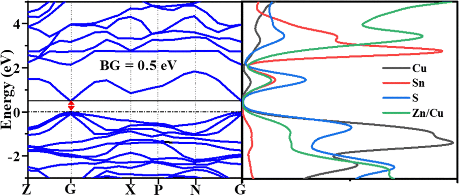 | ||
| Fig. 7 The band structure and density of states of the CZTS nanoparticles. | ||
The density of states (DOS) indicates that the electron from Cu dominates the VBM, and the CBM is by the S atoms. Furthermore, to identify in-depth, the site-projected DOS was observed for the Wyckoff positions (4d-Cu/Zn, 2a-Cu, 2b-Sn, 8i-S), as shown in ESI,† S2.
Notably, the CBM region is predominantly influenced by the Cu-3d electron from the 2a Wyckoff position. Similarly, in the same region, there is a significant contribution from the S 3p electrons, indicating the Cu–S bonding in the sample. Equally, in the CBM, Sn 5s and 5p-electrons and the S 3p dominate. The mixed 4d Zn/Cu position does not show a significant contribution at the Fermi level, but it showed a vital contribution below and above the Fermi level.
Fig. S3 (ESI†) depicts the calculated optical absorption spectra compared with the standard solar spectrum within the 200–800 nm range. The CZTS nanoparticles show a wide range of absorption of the UV-Vis spectral region. Notably, several absorption peaks were observed due to the electronic transitions between the VB and CB, which includes inter-band transition occurring in the ultraviolet-visible (UV-Vis) region. The transition includes the Cu 3d to S 3p electrons and Cu 3d to Sn 4s and 4p electronic transition from VB to CB. The identified optical absorption peaks match the standard solar spectrum range, supporting the sample's potential as a highly promising photoactive material, especially for photovoltaic applications.
(e) Electrochemical study
To study the lithium storage mechanism, cyclic voltammetry (CV) was carried out for the CZTS electrode, covering the potential range from 0.01 V to 3 V at a scan rate of 0.5 mV s−1. The CV profiles depicted in Fig. 8a and b illustrate the specific behaviour during the first 3 cycles. During the cathodic scan upon the initial lithiation, the cyclic voltammogram reveals four broad reduction peaks consistent with typical metal sulfide electrode behaviour. Notably, the four initial reduction peaks occurring around 2.5 V correspond to the lithiation of Li–CuxS alloys, while two additional peaks around the voltage range (1.4–1.6 V and 1.1 V to 0.8 V) are attributed to the involvement of Sn and Zn species in multistep reactions, as well as the formation of a solid electrolyte interface (SEI layer formation).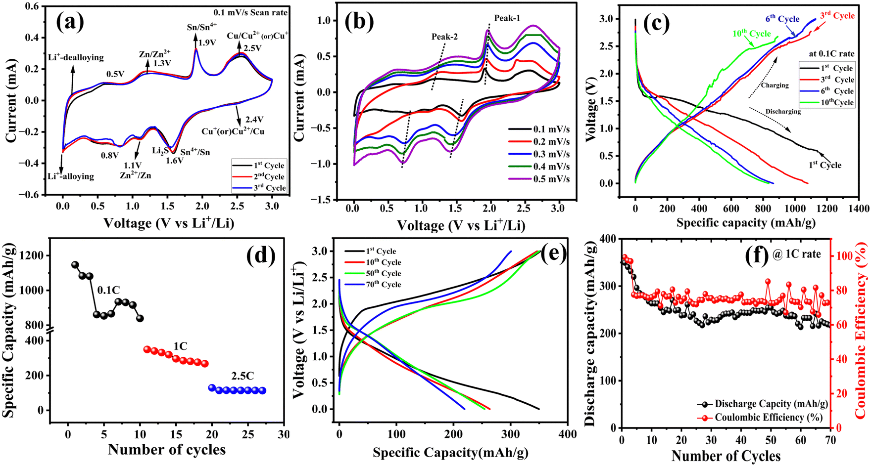 | ||
| Fig. 8 (a) CV curves for 3 cycles at 0.1 mV s−1 scan rate, (b) CV curves at different scan rates, (c) galvanostatic charge/discharge cycles of CZTS nanoparticles at 0.1C rate, (d) rate capability curves at C-rate from 0.1 to 2.5C, (e) galvanostatic charge/discharge at 2.5C rate and (f) cycling performance and coulombic efficiency at 1C rate. | ||
Moreover, the final reduction peak identified near 0.4–0.5 V is associated with the conversion reaction between Sn and Zn. In contrast, during the anodic scan, four oxidation peaks are evident at 0.55, 1.3, 1.9, and 2.5 V. The peak at 0.55 V corresponds to the de-lithiation of Sn and Zn alloy, while those at 1.3 and 1.9 V involve reversible reactions among Sn, Zn, and Li. The broad peak spanning 2.4 to 2.5 V can be assigned to the delithiation of Li–CuxS alloys and the oxidation of Li2S to S and lithium ions. Notably, the CV curves of the 2nd and 3rd cycles exhibit significant overlap, confirming the material's stability.37–39
Fig. 8(b) shows the CV at various scan rates ranging from 0.1 to 0.5 mV s−1 to understand the nanoparticle rate performance of the CZTS nanoparticles. The peak currents of the oxidation and the reduction peaks increase with the increase in the scan rates, which increases the peak potential difference between them. And it confirms that there is no significant deviation in the shape of the curves.
The electrochemical behaviour of the CZTS electrodes was investigated by galvanostatic charge/discharge cycles over the potential range of 0–3.0 V, as shown in Fig. 8(c). The CZTS electrodes showed a 1st cycle discharge capacity of 1143 mA h g−1, which is higher than the theoretical value of 847 mA h g−1 and corresponding discharge capacities of the 3rd, 6th, and 10th cycles are 1080, 864, and 833.3 mA h g−1. The charge capacities are 1100, 1128, and 891 mA h g−1, respectively at 0.1C rate. The high discharge capacity of the 1st cycle is more because of the hierarchical morphology with a large surface area of the CZTS nanoparticles, which will lead to a large amount of irreversible lithium insertion. Also, the extra capacity at the first discharge may be attributed to forming solid electrolyte interphase (SEI) layers on the electrolyte interface.23,40 The rate performance, cycling stability, and coulombic efficiency of the CZTS electrodes are illustrated in Fig. 8d–f. Fig. 8d displays the rate studies, showing initial discharge capacities of 1146.7, 350, and 129.3 mA h g−1 at different C rates of 0.1C, 1C, and 2.5C, respectively. Regarding cyclic stability, CZTS electrodes initially delivered a capacity of 350 mA h g−1 and maintained 221 mA h g−1 capacity after 70 cycles, even at a high scan rate of 1C, with a 73% coulombic efficiency (Fig. 8f). These results underline the excellent cycling performance and high-rate capability of the electrode materials, which are crucial for achieving high-performance lithium-ion batteries.
(f) Kinetic charge storage mechanism
A combined mechanism of faradaic and double-layer non-faradaic charge storage describes the area under the CV curve, requiring the identification of the dominant mechanism in electrochemical reactions for a complete knowledge of electrode material charge storage.Dunn and co-workers study provides a quantification technique for the charge storage mechanisms, where the total current is considered as the sum of capacitive and diffusion-controlled currents.41,42
| i(ν) = icapacitive + idiffusive | (1) |
The relation between the peak current (i) and the scan rate (v) obeys the power law.43
| ip = aνb | (2) |
Both a and b are variables that were adjustable parameters, and ip represents the Cathodic/Anodic peak current and ν denotes the sweep rate.44,45
For this, we take log on both sides of eqn (2), which gives:
| log(i) = blog(ν) + log(i) | (3) |
The b-values are calculated from the slope of the plot of logv vs. logi. There are two well-defined conditions: b = 0.5 and b = 1.0, whereas the value of b ranges from 0.5 to 1. If the value of b is around 0.5, then it is a diffusion-controlled process, and if it is close to 1, then it is a surface-capacitance-dominated process.46,47
The linear fitting of the logarithmic peak currents and scan rates was performed to obtain the value of parameter b, as shown in Fig. 9(a). The b values for the oxidation peak at 0.5 V and reduction peak at 0.3 V are 0.62 and 0.68 respectively. This value indicates that the lithium storage process of CZTS nanoparticles exhibits a transitive behaviour, which further confirms that the kinetics of the CZTS nanoparticles are a surface controlled capacitive process.
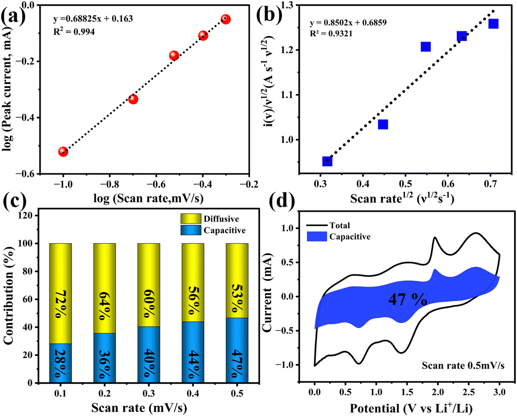 | ||
| Fig. 9 Kinetics and quantitative capacitive analysis of the lithium storage mechanism in the CZTS. (a) Relationship between logarithmic anodic peak currents and scan rates. (b) Plot of scan rate1/2 (V1/2 s−1) vs. i(v)/V1/2(A s−1 V1/2) for the anodic sweep. (c) Relative diffusion and capacitive contributions at different scan rates. (d) Pseudocapacitive contribution (shaded region) in the CV curve. | ||
Fig. 9(c) displays a histogram of the contribution of capacitance and diffusion behaviour to the total capacity, which was quantitatively studied at various scan rates. With an increase in the scan rate, the diffusion contribution was reduced, and the capacitive contribution increased. This increase in the capacitive contribution is due to the rapid lithium-ion diffusion across the whole cell and the small nanoscale size of the CZTS nanoparticles, which increases the specific surface area of the material and thereby shortens the lithium transport and diffusion path. The contribution of the capacitance to the total capacity at a specific scan rate of 0.5 mV s−1 was quantitatively analysed to be 46.7%, as shown in Fig. 9(d). This storage behaviour is due to the improved kinetics and charge transfer process of CZTS nanoparticles and is also in agreement with the higher value of parameter b denoting a much-enhanced capacitive kinetics.
(g) Counter electrode in DSSCs
For the construction of DSSC counter electrodes (CEs), the prepared CZTS material was mixed with TritonX 100 and was made into a paste-like consistency. The prepared paste was coated over the pre cleaned FTO substrates through the spin coating technique. The coated substrates were annealed at 350 °C under an argon atmosphere for one hour. The coating thickness was maintained to be 3–4 μm. N719 dye was used as a sensitizer for the preparation of the photo anode. The detailed construction of DSSC is given in the ESI.† To assess the functioning of the CZTS as counter electrodes in DSSCs, the Pt counter electrode as a control device was also studied. The constructed devices had an architecture of glass/FTO/compact-TiO2/porous-TiO2 with dye/electrolyte (Iodine based)/CZTS (or Pt)/FTO/glass. Fig. 10(a) depicts the J–V curves of the DSSCs constructed with the prepared CZTS and platinum as counter electrodes respectively. The device constructed with the CZTS as counter electrode exhibited comparable performance with that of platinum-based counter electrodes. The device with CZTS as the CE exhibited an open circuit voltage (VOC) of 0.71 V, which is comparable to the device made with Pt-based CEs with VOC of 0.72 V. The device exhibited a maximum current density of 13.6 mA cm−2 and fill factor of 61% (or 0.61) for CZTS-based CEs, and 13.9 mA cm−2 and 64% (or 0.64) for Pt-based CEs. From the J–V graph it can be inferred that the fill factor of the CZTS-based CEs was found to be slightly lower than that of the Pt-based CEs. This could be attributed to the higher series resistance in the device with the CZTS material than that of the Pt-based devices. The efficiency of the devices with CZTS and PT-based CEs was found to be comparable with efficiencies (η) of 5.9 and 6.4%, respectively. Comparing the cost efficiency of the CZTS-based material to noble metals makes it a potential candidate as a DSSC CE. Fig. 10(b) shows the IPCE spectra of the DSSC prepared with Pt and CZTS as counter electrodes. The IPCE response was observed to be in accordance with the Jsc values obtained from the J–V results.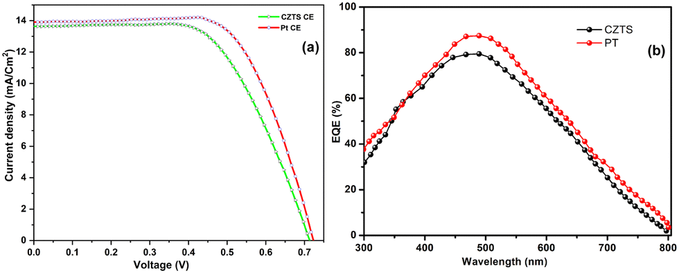 | ||
| Fig. 10 Photocurrent density–voltage (a) and IPCE (b) curves of the DSSCs prepared with CZTS and Pt-based counter electrodes. | ||
Conclusion
In conclusion, this research article explores the electrochemical activity and potential application of quaternary semiconducting material Cu2ZnSnS4 (CZTS), as an alternative anode material for lithium-ion batteries and as counter electrodes in DSSCs. CZTS nanoparticles were synthesized via a cost-effective solvothermal method, and their structural properties were confirmed using X-ray diffraction and Raman spectroscopy. X-ray photoelectron spectroscopy was employed to determine the stoichiometry and oxidation states of CZTS. It also exhibited a higher surface area of 34.2 m2 g−1, which led to a large amount of irreversible lithium insertion and a higher degree of uniformity in the range of 3.3 nm. Field-emission scanning electron microscopy revealed the formation of CZTS nanoflakes, and their electrochemical properties showed their potential for high cycling stability and exhibited an initial discharge capacity of 1141.08 mA h g−1, 350 mA h g−1 at the scan rate of 0.1C and 1C. The charge storage mechanism revealed the surface dominant behaviour of the CZTS material. This study highlights CZTS as a promising, earth-abundant, and low-cost anode material for next-generation lithium-ion batteries and as a counter electrode for DSSCs.Author contributions
G. Rajesh – conceptualization; data curation; investigation; methodology, writing – original draft; project administration. Jeyakiruba Palraj – conceptualization; data curation; investigation, software, writing – original draft. M. R. Venkatraman – investigation, methodology, writing. Ramesh Sivasamy – software, writing review. Sreejith P. Madhusudanan – writing review – editing, Helen Annal Therese – supervision, resources, writing reviewing – editing, Marcos Flores – project administration, supervision, writing review – editing.Conflicts of interest
There are no conflicts to declare.Acknowledgements
The author G. Rajesh would like to thank the ‘Conicyt FONDECYT (Fondo Nacinal de Desarrollo Científico y Tecnológico)’ Postdoctrado Project No. 3190647 for the research support.References
- M. Yildirim and Z. Candan, Mater. Today: Proc., 2023 DOI:10.1016/j.matpr.2023.10.116.
- C. Liu, Q. Lu, J. Qu, W. Feng, A. Thomas, Y. Li, I. G. G. Martinez, C. Pan and D. Mikhailova, Small, 2024, 2311253 CrossRef PubMed.
- Q. Lu, C. Liu, Y. Zhao, W. Pan, K. Xie, P. Yue, G. Zhang, A. Omar, L. Liu, M. Yu and D. Mikhailova, SusMat, 2023, 3, 471–497 CrossRef CAS.
- C. M. MacLaughlin, ACS Energy Lett., 2019, 4, 786–788 CrossRef CAS.
- A. Manthiram, J. Phys. Chem. Lett., 2011, 2, 176–184 CrossRef CAS.
- Z. Syum, T. Billo, A. Sabbah, A. Kumar Anbalagan, S. Quadir, A. G. Hailemariam, P. Sabhapathy, C.-H. Lee, H.-L. Wu and L.-C. Chen, Chem. Eng. J., 2023, 465, 142786 CrossRef CAS.
- J.-M. Tarascon and M. Armand, Nature, 2001, 414, 359–367 CrossRef CAS PubMed.
- J. Yang, C.-Y. Wang, C.-C. Wang, K.-H. Chen, C.-Y. Mou and H.-L. Wu, J. Mater. Chem. A, 2020, 8, 5095–5104 RSC.
- E. Kamali-Heidari, A. Kamyabi-Gol, M. Heydarzadeh Sohi and A. Ataie, J. Ultrafine Grained Nanostruct. Mater., 2018, 51, 1–12 Search PubMed.
- D. Deng, Energy Sci. Eng., 2015, 3, 385–418 CrossRef.
- H. Wu and Y. Cui, Nano Today, 2012, 7, 414–429 CrossRef CAS.
- M. N. Obrovac and V. L. Chevrier, Chem. Rev., 2014, 114, 11444–11502 CrossRef CAS PubMed.
- B. Liang, Y. Liu and Y. Xu, J. Power Sources, 2014, 267, 469–490 CrossRef CAS.
- Y. Jin, B. Zhu, Z. Lu, N. Liu and J. Zhu, Adv. Energy Mater., 2017, 7, 1700715 CrossRef.
- J. R. Szczech and S. Jin, Energy Environ. Sci., 2011, 4, 56–72 RSC.
- H. E. Wang, L. J. Xi, R. G. Ma, Z. G. Lu, C. Y. Chung, I. Bello and J. A. Zapien, J. Solid State Chem., 2012, 190, 104–110 CrossRef CAS.
- J. Li, J. Shen, Z. Li, X. Li, Z. Sun, Z. Hu and S. Huang, Mater. Lett., 2013, 92, 330–333 CrossRef CAS.
- P. V. Prikhodchenko, Y. Denis, S. K. Batabyal, V. Uvarov, J. Gun, S. Sladkevich, A. A. Mikhaylov, A. G. Medvedev and O. Lev, J. Mater. Chem. A, 2014, 2, 8431–8437 RSC.
- D. Y. Yu, P. V. Prikhodchenko, C. W. Mason, S. K. Batabyal, J. Gun, S. Sladkevich, A. G. Medvedev and O. Lev, Nat. Commun., 2013, 4, 2922 CrossRef PubMed.
- K. T. Lee, Y. S. Jung and S. M. Oh, J. Am. Chem. Soc., 2003, 125, 5652–5653 CrossRef CAS PubMed.
- H. A. Patel, F. Karadas, A. Canlier, J. Park, E. Deniz, Y. Jung, M. Atilhan and C. T. Yavuz, J. Mater. Chem., 2012, 22, 8431–8437 RSC.
- M. G. Kim, S. Sim and J. Cho, Adv. Mater., 2010, 22, 5154–5158 CrossRef CAS PubMed.
- W.-H. Zhou, Y.-L. Zhou, J. Feng, J.-W. Zhang, S.-X. Wu, X.-C. Guo and X. Cao, Chem. Phys. Lett., 2012, 546, 115–119 CrossRef CAS.
- J. Jin, S.-Z. Huang, J. Liu, Y. Li, L.-H. Chen, Y. Yu, H.-E. Wang, C. P. Grey and B.-L. Su, Adv. Sci., 2015, 2, 1500070 CrossRef PubMed.
- J. Jin, S.-Z. Huang, Y. Li, H. Tian, H.-E. Wang, Y. Yu, L.-H. Chen, T. Hasan and B.-L. Su, Nanoscale, 2015, 7, 12979–12989 RSC.
- S.-Z. Huang, Y. Cai, J. Jin, J. Liu, Y. Li, H.-E. Wang, L.-H. Chen, T. Hasan and B.-L. Su, J. Mater. Chem. A, 2016, 4, 4264–4272 RSC.
- X. Yang, J. Xu, L. Xi, Y. Yao, Q. Yang, C. Y. Chung and C.-S. Lee, J. Nanopart. Res., 2012, 14, 931 CrossRef.
- J. Gong, K. Sumathy, Q. Qiao and Z. Zhou, Renewable Sustainable Energy Rev., 2017, 68, 234–246 CrossRef CAS.
- H.-E. Wang, L.-X. Zheng, C.-P. Liu, Y.-K. Liu, C.-Y. Luan, H. Cheng, Y. Y. Li, L. Martinu, J. A. Zapien and I. Bello, J. Phys. Chem. C, 2011, 115, 10419–10425 CrossRef CAS.
- G. N. Ngubeni, O. Akinbami, L. Mxakaza, S. Nkabinde, T. Kolokoto, F. Otieno, M. J. Moloto, K. P. Mubiayi and N. Moloto, Thin Solid Films, 2022, 745, 139099 CrossRef CAS.
- Y. Tan, D. Fang, N. Cheng, F. Xiong, W. Ding, B. Mi and Z. Gao, Mater. Sci. Semicond. Process., 2023, 166, 107710 CrossRef CAS.
- Q. Guo, H. W. Hillhouse and R. Agrawal, J. Am. Chem. Soc., 2009, 131, 11672–11673 CrossRef CAS PubMed.
- K.-C. Wang, P. Chen and C.-M. Tseng, CrystEngComm, 2013, 15, 9863–9868 RSC.
- P. Fernandes, P. Salomé and A. Da Cunha, J. Alloys Compd., 2011, 509, 7600–7606 CrossRef CAS.
- S. Ji, T. Shi, X. Qiu, J. Zhang, G. Xu, C. Chen, Z. Jiang and C. Ye, Sci. Rep., 2013, 3, 2733 CrossRef PubMed.
- S. Ahmadi, N. Khemiri, A. Cantarero and M. Kanzari, J. Alloys Compd., 2022, 925, 166520 CrossRef CAS.
- B. Qu, H. Li, M. Zhang, L. Mei, L. Chen, Y. Wang, Q. Li and T. Wang, Nanoscale, 2011, 3, 4389–4393 RSC.
- S. Saadat, Y. Y. Tay, J. Zhu, P. F. Teh, S. Maleksaeedi, M. M. Shahjamali, M. Shakerzadeh, M. Srinivasan, B. Y. Tay and H. H. Hng, Chem. Mater., 2011, 23, 1032–1038 CrossRef CAS.
- B. Qu, M. Zhang, D. Lei, Y. Zeng, Y. Chen, L. Chen, Q. Li, Y. Wang and T. Wang, Nanoscale, 2011, 3, 3646–3651 RSC.
- Q. Jiang, X. Chen, H. Gao, C. Feng and Z. Guo, Electrochim. Acta, 2016, 190, 703–712 CrossRef CAS.
- J. Wang, J. Polleux, J. Lim and B. Dunn, J. Phys. Chem. C, 2007, 111, 14925–14931 CrossRef CAS.
- T. Brezesinski, J. Wang, S. H. Tolbert and B. Dunn, Nat. Mater., 2010, 9, 146–151 CrossRef CAS PubMed.
- L. Wang, T. Zhao, R. Chen, H. Fang, Y. Yang, Y. Cao and L. Zhang, Batteries, 2023, 9, 32 CrossRef CAS.
- Zhou Huang, Y.-B. Cheng and R. A. Caruso, Chem. Mater., 2006, 18, 5835–5839 CrossRef.
- S. R. Das, S. B. Majumder and R. S. Katiyar, J. Power Sources, 2005, 139, 261–268 CrossRef CAS.
- T. Zhu, Y. Wang, Y. Li, R. Cai, J. Zhang, C. Yu, J. Wu, J. Cui, Y. Zhang, P. M. Ajayan and Y. Wu, ACS Appl. Nano Mater., 2020, 3, 10369–10379 CrossRef CAS.
- J. B. Cook, H.-S. Kim, Y. Yan, J. S. Ko, S. Robbennolt, B. Dunn and S. H. Tolbert, Adv. Energy Mater., 2016, 6, 1501937 CrossRef.
Footnotes |
| † Electronic supplementary information (ESI) available. See DOI: https://doi.org/10.1039/d4ya00135d |
| ‡ These authors contributed equally to this work. |
| This journal is © The Royal Society of Chemistry 2024 |