
 Open Access Article
 This Open Access Article is licensed under a Creative Commons Attribution-Non Commercial 3.0 Unported Licence
Optical properties enhancement via WSSe/silicene solar cell junctions†
Renan Narciso
Pedrosa
 *a,
Cesar E. P.
Villegas
c,
A. R.
Rocha
d,
Rodrigo G.
Amorim
b and
Wanderlã L.
Scopel
a
*a,
Cesar E. P.
Villegas
c,
A. R.
Rocha
d,
Rodrigo G.
Amorim
b and
Wanderlã L.
Scopel
a
aDepartamento de Física, Universidade Federal do Espírito Santo – UFES, Vitória/ES, Brazil. E-mail: renannarcisopedrosa@gmail.com; wanderla.scopel@ufes.br
bDepartamento de Física, ICEx, Universidade Federal Fluminense – UFF, Volta Redonda/RJ, Brazil. E-mail: rgamorim@id.uff.br
cDepartamento de Ciencias, Universidad Privada del Norte, Lima 15434, Peru. E-mail: cesar.perez@upn.edu.pe
dInstituto de Física Teórica, Universidade Estadual Paulista (UNESP), Rua Dr. Bento T. Ferraz, 271, São Paulo, SP 01140-070, Brazil. E-mail: alexandre.reily@unesp.br
First published on 4th March 2024
Abstract
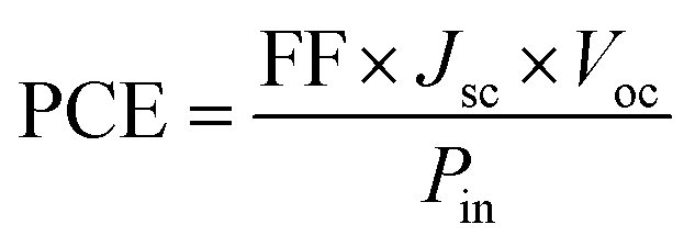
2D Janus monolayers exhibit nanoscale asymmetric surface organization along the out-of-plane direction and have recently emerged as a class of 2D materials. In this work, we investigate the energetic, electronic, and optical properties of the vertical van der Waals stack between WSSe and silicene monolayers based on first-principles calculations. The Janus/silicene interface formation is driven by an exothermic process, and charge transfer from the silicene to the Janus monolayer is observed. The intrinsic properties of silicene and Janus are preserved despite the stacking of the parts. The Bethe–Salpeter equation (BSE) was used to understand the contact influence on the optical absorption spectrum of the vertical interface. Our findings reveal that the power conversion energy (PCE) of the heterostructure is boosted 2.42 times higher than that of the Janus monolayer. Thus, due to its PCE and transparent electrical contact, the heterojunction is a promising candidate for use as a photovoltaic device compared to its counterparts.
1 Introduction
Since the first successful realization of graphene, the quest for 2D materials with improved physical and chemical properties has attracted considerable attention, due to their potential device applications in electronics,1–3 plasmonics,4 optoelectronics5 and photovoltaics.6–9 Indeed, within the novel catalog of materials, one can find semimetallic materials (silicene,10–14 germanene15) and semiconductors such as phosphorene,16,17 Xenes,18,19 and transition metal dichalcogenides (TMDCs).20 The latter have been reported as promising materials for application in photo-electronic devices21 due to their direct bandgap energy and large optical absorption.More recently, Janus monolayers of TMDCs – a new family of 2D semiconductors with the chemical formula MXY and obtained by Y-implantation in the MXY (X ≠ Y) (M = Mo, W, Pt; X = S, Se, Sn and Te and Y = S, Se, Sn and Te), have been synthesized by chemical vapor deposition (CVD) techniques,22,23 opening new avenues towards novel electronic applications due to the presence of intrinsic electric fields in the material, a direct consequence of the symmetry breaking during the substitution process. In particular, Janus MoSSe, PtSSe, and SnSSe monolayers have already been shown to be potential candidates for solar cells and optoelectronic devices.24–26 Furthermore, Ting Zheng et al.27 demonstrated experimentally (at 300 K) that WSSe and MoSSe have longer recombination lifetimes with faster exciton formation times compared to their conventional TMDs. These peculiar properties are attributed to the reduced overlap of the electron and hole wave functions caused by the intrinsic dipole moment. This not only facilitates charge separation but also charge collection, opening up new avenues for photodetection and photovoltaic applications. For p–n junctions, recent theoretical works have explored vertical stacking between Janus monolayers with type II band alignment, and they have found high power conversion efficiency (PCE) values.28–31
The metal–semiconductor interface plays an important role in electronic and optoelectronic devices. A recent experimental study has demonstrated that a metal (2D)–semiconductor interface enhances the efficiency of photovoltaic nanodevices,32 since the Fermi level pinning33 decreases or disappears compared to a metal (3D)/semiconductor interface.34 A semi-metal material that has high integration with silicon (used in the production of photovoltaic cells) and that has attracted attention is silicene. This material shares many of the intriguing electronic properties of graphene, such as the Dirac cone, high Fermi velocity and carrier mobility.10–12 Unlike graphene, a silicene sheet is periodically buckled, which makes it more flexible. Furthermore, recent experimental work has demonstrated the feasibility of growing a silicene sheet using 2D-MoS2 as a substrate.35 This discovery has opened new avenues, leading to the proposal of various silicene/semiconductor interfaces as potential 2D platforms for optoelectronic nanodevices.36–38 Among these, Kharadi et al.39,40 propose a silicene/MoS2 heterojunction, which has shown improved performance in MoS2-based photodetectors. The enhancement observed can be attributed to the high carrier mobility in silicene, which reduces the transit time of the photodetectors. As a result, the silicene/MoS2 interface exhibits higher responsivity and photoconductive gain compared to graphene-based devices.
In this work, we employ hybrid first-principles calculations to investigate the electronic, interface formation, and optical properties of vdW vertical heterostructures based on WSSe/Si. Our results demonstrate that the intrinsic properties of silicene and the Janus material are preserved regardless of the stacking pattern performed between the parts. Moreover, we find that the WSeS/Si interface forms a n-type Schottky contact that can be converted into p-type under the substitution of the dichalcogenide atom that is localized on top of the Si atom. The optical absorption of the interface and its constituent is subsequently studied, fully including excitonic effects. Finally, based on the results of the optical constants, we estimate the WSSe/Si Schottky contact solar cell performance, finding improved efficiency and photogenerated current with respect to its individual constituent parts.
2 Methodology and computational details
The calculations of the energetic and structural system's properties were performed by using density functional theory (DFT) as implemented in the QUANTUM ESPRESSO package.41 The exchange–correlation energy was obtained within the generalized gradient approximation, as proposed by Perdew, Burke, and Ernzerhof (GGA-PBE),42 and van der Waals (vdW) interactions were included using the Grimmer-D2 approach.43 However, for the electronic properties of both the isolated and heterojunction systems, the hybrid functional HSE06 was used.44The isolated monolayers and the silicene/Janus interface consist of a 2 × 2 × 1 supercell with a vacuum region of 17 Å. The Brillouin zone sampling was carried out in a 12 × 12 × 1 k-point mesh, and the Kohn Sham orbitals were expanded on a plane-wave basis set with an energy cutoff of 80 Ry. Atomic relaxation was performed until the residual forces approached 2.5 meV Å−1. The energetic stability of the heterostructure was explored by ab initio molecular dynamic (AIMD) calculations using the Vienna ab initio simulation package (VASP).45,46 The AIMD calculations were performed using the Nosé thermostat method47 at 300 K for a total time of 10 ps.
The optical spectrum is obtained by solving the Bethe–Salpeter equation (BSE), as implemented in the YAMBO code.48 The BSE can be reduced to an eigenvalue problem of the Hamiltonian,
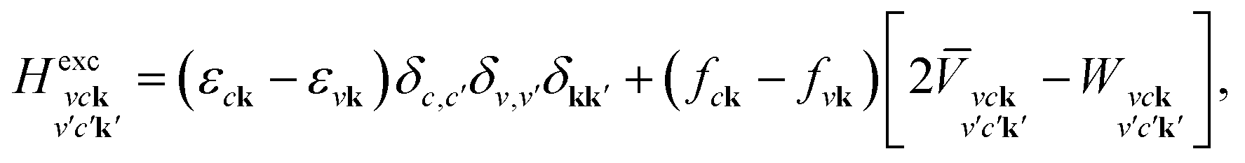 | (1) |
 is the BSE kernel. Its first term corresponds to the electron–hole exchange part from the Hartree potential, while the second term represents the electron–hole attraction part from the screened exchange potential. Within the Tamm–Dancoff approximation,49 the macroscopic dielectric function can be expressed as
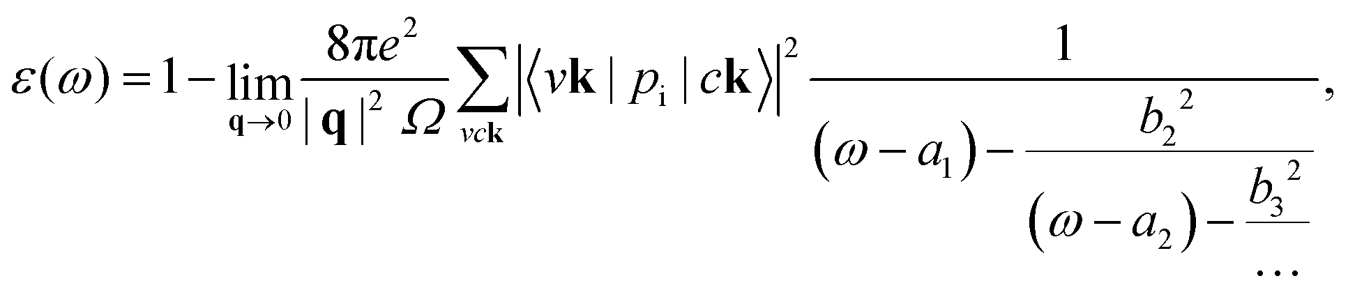 | (2) |
Given the two-dimensional nature of our systems, we employ the slab Coulomb truncation scheme along the c-direction during the computation of the screened potential. For the single layer systems, the dielectric function was generated on a k-grid sample of 54 × 54 × 1 (see ESI† for the convergence tests). The quasiparticle corrections were included via a scissor operator, whose value was set based on the HSE06 hybrid functional, following the procedure described in ref. 50. In order to better resolve the optical spectrum, we take advantage of the double-grid approach,51 where the electron–hole kernel matrix elements are calculated in a course grid and then interpolated on a fine mesh of 180 × 180 × 1 for the monolayer systems and 90 × 90 × 1 for the interface. Five valence bands and five conduction bands were included for WSSe, while for silicene three valence bands and four conduction bands were included. For the heterostructure, we employ 16 valence bands and 15 conduction bands. We verify that the inclusion of more bands does not change the optical response in the visible spectrum. The number of G-vectors and block size employed to calculate the screened electron–hole interaction, expressed in energy units, were 10 and 4 Ry, respectively. In all our calculations, we consider light polarized parallel to the plane of the layers, and an artificial Lorentzian broadening of 0.05 eV to smear out the optical response.
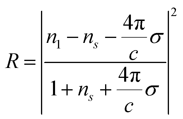
The optical constants, i.e., the transmittance (T), reflectance (R), and absorptance (A), were obtained from the real and imaginary parts of the dielectric function and considering Fresnel's relations for atom-thick films,52,53
 | (3) |
 | (4) |
| A = 1 − R − T. | (5) |
Here, n1 and ns are the refractive index of the incident and transmitted medium, and 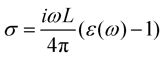 is the optical surface conductivity of a system with thickness L. The refractive indices n1 and ns correspond to air and glass, respectively. In our calculations, we adopted the experimental conditions reported by Morozov et al.54 and assumed bulk interlayer spacings as the effective thickness of the monolayer samples, while for the interface we used a 1 nm thickness.
We evaluated the maximum power conversion efficiency (PCE) of the proposed systems, following the approach proposed by de Vos,55
 | (6) |
 | (7) |
| J = Jsc − J0(eeV/kBT − 1) | (8) |
 | (9) |
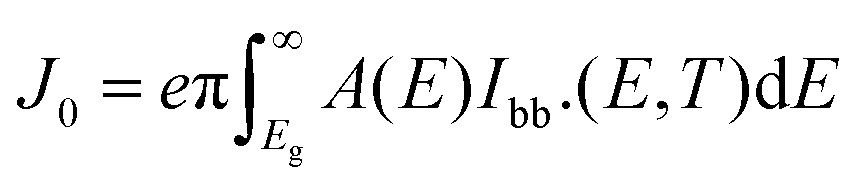 | (10) |
Here, e is the electron charge, and Eg represents the optical gap of the active absorber material.
The open circuit voltage is computed as the value of the voltage at which the device net current density vanishes, which yields the relation
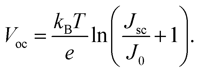 | (11) |
In this work, we treat the interface as a single junction and consider the optical losses due to reflection. Hence, the PCE methodology is able to provide reliable upper limits for the PCE.
3 Results and discussion
The WSSe Janus monolayer was constructed by replacing one of the Se atoms by S in the unit cell of the Wse2 structure. We find a formation energy59 of −0.88 eV per unit cell, which is a signature of an exothermic process. Here, we used the S(Se) source chemical potential from the bulk phase.In Fig. 1a, we show the fully relaxed hexagonal structure for monolayer Janus WSSe, highlighting the unit cell. Our results provide a lattice parameter of 3.26 Å, and W–S (W–Se) bond lengths of 2.42 Å (2.54 Å). Fig. 1b depicts the atomic structure of the silicene monolayer, with a lattice parameter of 3.85 Å and the out-of-plane low buckling value of ΔLB = 0.47 Å. Overall, our results agree with previous studies10,60–62 and are summarized in Table 1. To verify the thermodynamic stability, we calculated the phonon spectra for Janus and silicene, and no negative frequencies were observed (see ESI†).
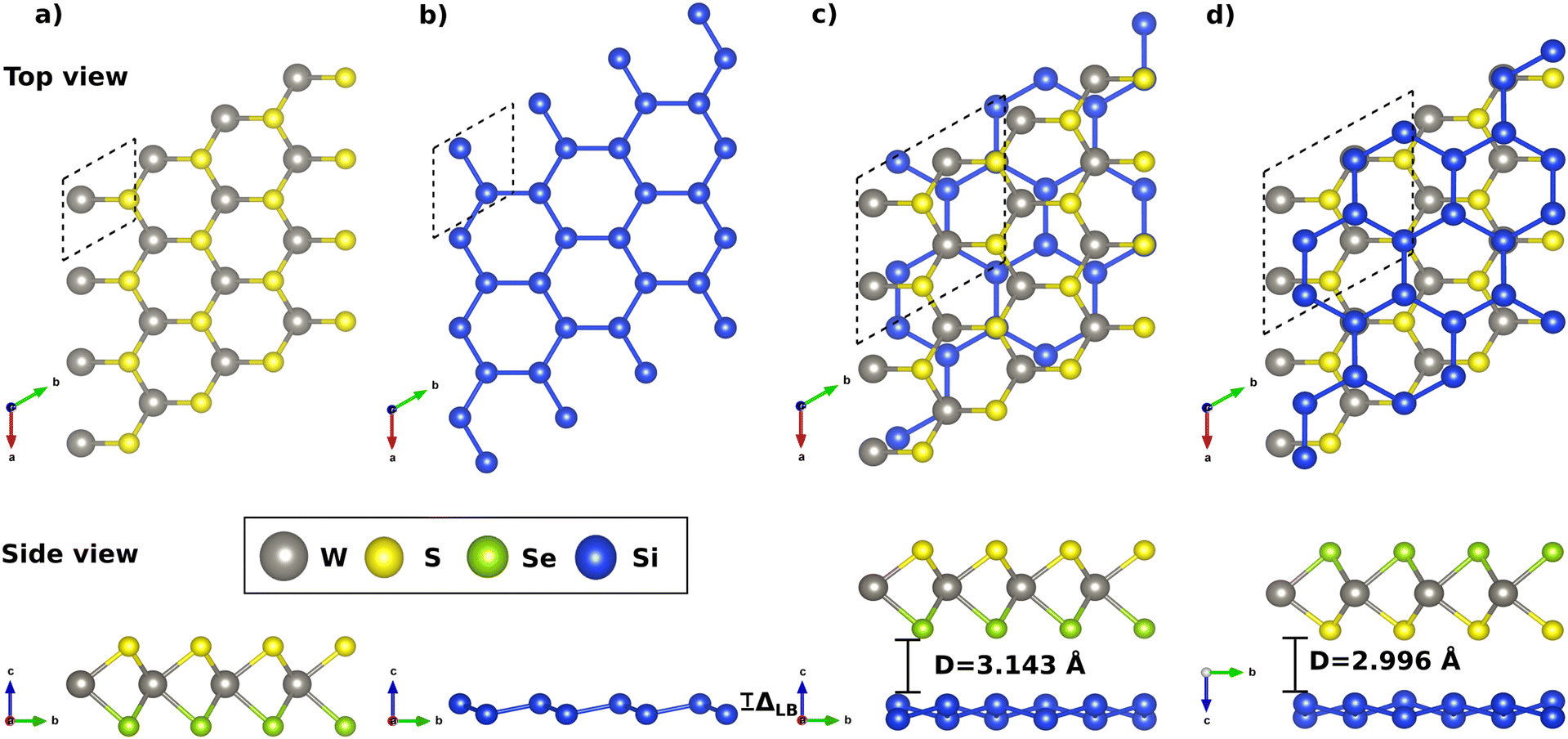 | ||
| Fig. 1 The fully relaxed geometries are shown, where (a) represents the WSSe Janus monolayer, (b) the silicene monolayer, and (c) and (d) the WSSe/Si (Se atoms are the shortest distance from Si atoms) and WSeS/Si (S atoms are the shortest distance from Si atoms) heterostructures, respectively. | ||
Next, we constructed a vertical heterostructure composed of silicene and WSSe monolayers as shown in Fig. 1c and d. For nominating the structures, when S(Se) atoms are close to Si, we will call it from now on WSeS/Si (WSSe/Si). The heterostructure mismatch is 2.3%, where the silicene was rotated by 30 degrees and compressed. To assess the interface formation, we determined the binding energy63 and found −18.4, and −17.4 meV Å−2 for WSSe/Si and WSeS/Si, respectively. These results are comparable with previous results obtained for graphene in contact with WSSe64 and WSeTe.65
The interlayer distance between WSeS and Si (WSSe and Si) was found to be 3.00 (3.14) Å, and the value of ΔLB increased by 20% due to interface formation. These results reveal that the interaction between the surfaces is governed by van der Waals forces. Analyzing the charge transfers in the interface formation, we noted that silicene transfers charge to the Janus, as shown in Table 1. Indeed, it is verified that the transference is higher in the WSeS/Si case.
For the heterostructure (WSSe/Si), phonon dispersion calculations were conducted (see ESI† Fig. S4). No negative frequencies were observed, indicating the stability of the structure. In addition, an AIMD simulation was performed in order to study the thermal stability at room temperature. The total energy fluctuation time evolution is shown from 1 to 10 ps of the WSSe/Si hetero-sheets (see ESI† Fig. S3). The structure remains without a broken bond or significant structural deformation, confirming the stability of the Janus/Si nano-structure system at 300 K.
Considering the Janus structural stability, Fig. 2a shows the band structure for the pristine WSSe sheet. We can note a semiconductor character with an electronic direct band gap Eg = 2.12 eV comparable with previous works.29,66 In addition, we also found an optical gap (BSE) close to 1.90 eV with a deviation of 2.43% relative to the experimental data.23,27 Moreover, the conduction band minimum (CBM) and valence band maximum (VBM) are ascribed to the hybridization of the W-d and Se-p orbitals, with a minority contribution of S-p, as reported previously.67Fig. 2b depicts the silicene band structure, which is a semimetal, with crossing bands at the Γ-symmetry point.10,68Fig. 2c and d show the electronic energy bands of the WSSe/Si and WSeS/Si heterostructures, respectively. Of note, at Γ there is a degeneracy break due to the interaction of the silicene and Janus. It is also observed at the K–M points an indirect bandgap for WSSe/Si; on the other hand, a direct one for WSeS/Si due to the Janus (majority W-d) state contributions.
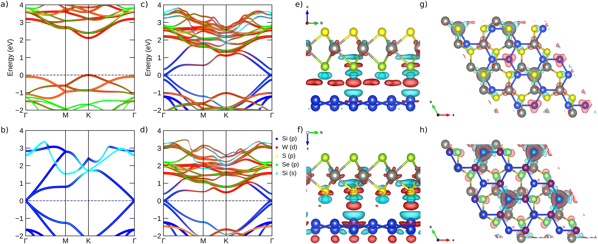 | ||
Fig. 2 The band structure projections (using HSE06) considering only orbitals that had a contribution greater than 3% of the maximum total density of states for (a) the WSSe Janus geometry,58 (b) 30 degree rotated silicene,12 (c) WSSe/Si and (d) WSeS/Si; (e)–(g) and (f)–(h) the side and top views of the charge density redistribution for WSSe/Si (WSeS/Si); Δρ(![[r with combining right harpoon above (vector)]](https://www.rsc.org/images/entities/i_char_0072_20d1.gif) ) > 0 and Δρ() < 0 are represented by light red and cyan colors, respectively. Isosurface 0.0006 e Å−3. ) > 0 and Δρ() < 0 are represented by light red and cyan colors, respectively. Isosurface 0.0006 e Å−3. | ||
To better understand the interaction between the Janus and silicene sheets, we calculated the charge density difference (Δρ), which represents how the charge is redistributed, when one compares the combined system with its isolated counterparts. We define Δρ() as:
| Δρ() = ρhetero() − (ρjanus() + ρsilicene()), | (12) |
) is the hetero-junction total charge, ρjanus() is the total charge density of the Janus and ρsilicene() is the total charge density of silicene. Fig. 2e and f show the charge density redistribution for WSSe/Si and WSeS/Si due to the formation of the interfaces, respectively. One can note a redistribution of charge density between both interfaces. A higher density charge deficit in the silicene layer for the WSeS/Si interface compared to WSSe/Si is observed, which is in accordance with Bader's analysis (see Table 1). Consequently, charge density is accumulated in the region between Se/Si and S/Si as indicated by the red isosurfaces in Fig. 2e and f. Furthermore, we also verified that Se (WSSe/Si) gains 0.044e, and S (WSeS/Si) also gains 0.094e, as depicted in Fig. 2e and f, respectively.
Analysing the charge transfer across the silicene-2D/semiconductor interface, an interface dipole is observed (see Fig. 2e and f), as already reported in previous works.69–71 Thus, to determine the n-type (ΦBn) and p-type (ΦBp) Schottky barrier heights (SBH), we have used the following expression:64
| ΦBn = WSi + ΔV − χint | (13) |
| ΦBp = Iint − WSi − ΔV | (14) |
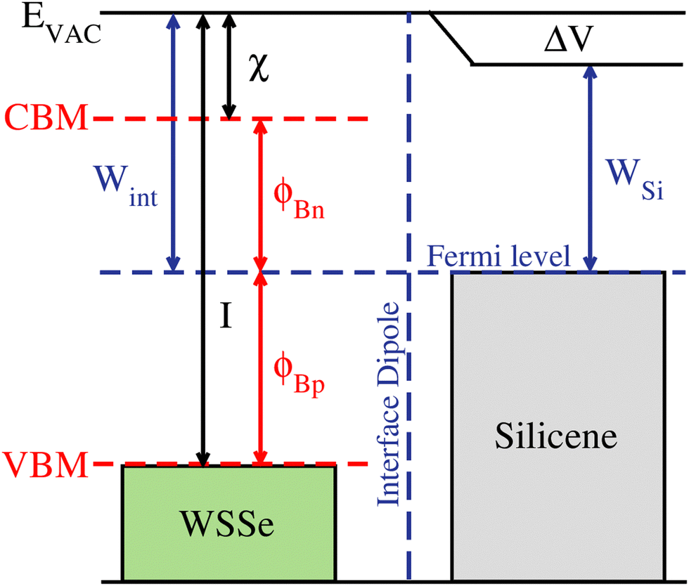 | ||
| Fig. 3 Schematics of the silicene/Janus heterojunction. Evac is the vacuum level and the horizontal blue dashed lines are the Fermi level Ef of the interface. The WSi (Wint) is the work function of the silicene (interfaces), χ (I) is the electron affinity (ionization potential) of the WSSe and the ϕBn (ϕBp) are the n-type (p-type) Schottky barrier height. | ||
Our results for both interfaces are similar to those previously reported in a graphene/MoS2 interface,8 where it is argued that due to the large energy barrier for holes (greater than 1 eV), the diffusion of these carriers from the semiconductor to silicene would be hampered, which may be beneficial for improving the current density in a prototypical photovoltaic device based on these interfaces.
Hereafter, we focus on the optical properties of the WSSe/Si interface to explore its photovoltaic potential. In contrast to previous works that calculate the absorptance by using the relation,  ,8,72 which relies on the assumption of zero reflection at the absorber's surface, herein we calculate the optical constants considering Fresnel's relations for atom-thick films.
In Fig. 4a we show the absorptance of silicene, WSSe and the WSSe/Si interface. We observe that silicene presents an intense peak at 3.7 eV and absorbs up to 2.9% of visible light. This intense peak is related to optical transitions around the Γ-point.73,74 Notice that due to excitonic effects, the optical transitions originating around the M-point are heavily suppressed, which agrees with a previous study conducted at the same level of theory.75 In addition, the WSSe monolayer presents the first excitonic state at ∼1.89 eV, which is in close agreement with recent experimental measurements.27 In the energy range shown, the Janus monolayer absorbs a maximum of 7.3% of light. Overall, our simulated excitonic spectra for WSSe describe fairly well both the peak positions and intensities. Concerning the interface, we observe the presence of three peaks with enhanced intensities that result from the hybridization of the bands along the K–Γ path (see Fig. 2c). Thus the interface absorbs up to 13.5% of light in the visible region, which doubles the maximum value absorbed by the WSSe monolayer. The inset shows the transmittance and reflectance of the WSSe/Si interface. There one can clearly see that in the visible range, the interface presents a nearly constant reflectance of ∼5%, whereas the lower bound for transmittance is ∼78% at light energy of ∼3.7 eV. This set of results highlights the improved absorption performance of the proposed interface with respect to the isolated monolayers.
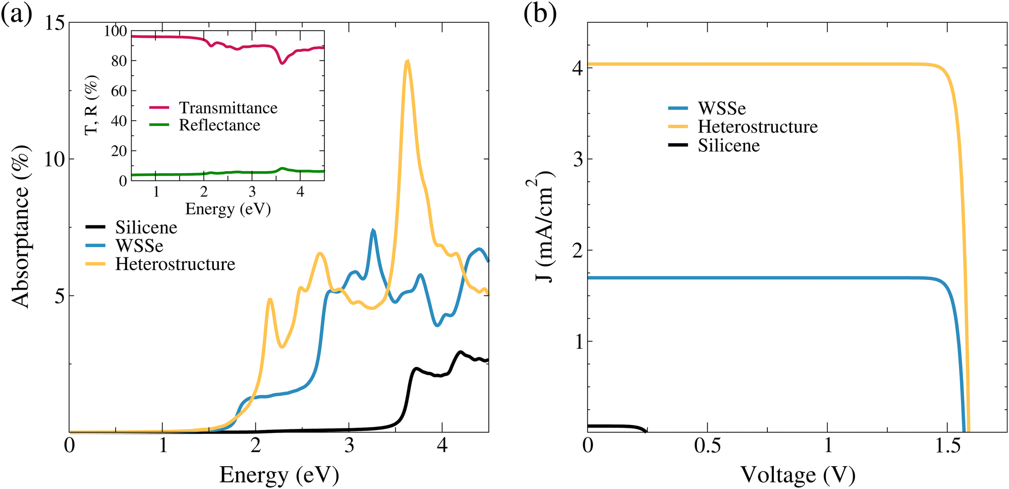 | ||
| Fig. 4 (a) Optical absorptance of monolayer WSSe (blue), silicene (black), and the WSSe/Si interface (yellow). (b) Current density as a function of voltage for the three studied systems. The inset shows the transmittance (red) and reflectance (green) of the WSSe/Si interface. | ||
In Fig. 4b, we show the net photoabsorbed current density as a function of the delivered voltage. Clearly, the current density of the interface doubles the value of the isolated Janus monolayer. On the other hand, Voc of the interface is 1.56 V, which is slightly larger than the WSSe case (1.53 V). In addition, we find a maximum PCE of 2.4% and 5.8% for WSSe and the interface, respectively. The maximum efficiency of the proposed WSSe/Si interface is ∼6 times greater than an interface based on graphene/MoS2.8 This considerable improvement can be ascribed to the fact that graphene absorbs almost 2.3% of light for photon energies above 4.3 eV, whereas silicene can absorb effectively for values above 2.2 eV.
It should be mentioned that there have been other theoretical proposals addressing the electronic and photovoltaic properties in type-II Janus heterojunctions,28–31 showing that under certain particular energy band offsets and energy band gaps, these Janus-based heterojunctions can reach power conversion efficiencies (PCEs) that may triple the predicted values of our Janus-based interface. Nevertheless, the comparison of the photovoltaic properties of these interfaces with ours should be done with care, as we are dealing with a metal–semiconductor interface that forms a Schottky barrier. While our system is, in principle, able to reduce Fermi level pinning and facilitate the diffusion of carriers (electrons or holes) towards the electrodes of a photovoltaic device, as suggested by experimental studies, the type-II heterojunctions facilitate exciton dissociation and charge separation at the interface. In this regard, we believe that the two systems are complementary in the sense that a type-II Janus heterojunction could achieve high efficiencies, but they eventually require metallic electrodes. Here we show that it is possible to engineer this arrangement to increase efficiency even further.
Finally, we mention that experimental measurements of the photovoltaic response in graphene/TMDCs heterostructures76 have demonstrated that the external quantum efficiency of this type of device can be enhanced from 2.4%, which corresponds to a monolayer, to up to 34% for multilayer semiconductor absorbers. Based on this result, we argue that the efficiency of the interface reported here can be significantly enhanced by increasing the thickness of the Janus semiconductor.
4 Conclusions
In summary, based on quantum mechanics calculations, we investigate the structural and electronic properties of the van der Waals vertical stack between WSSe and a silicene sheet. Our results demonstrate that the intrinsic properties of silicene and Janus are preserved regardless of the stacking pattern performed between the parts. Moreover, we found that the vertical hetero-structure presents a metallic character with the Fermi level crossed by bands associated with p-orbitals of the silicon atoms. From the solution of the Bethe–Salpeter equation, it was possible to investigate the contact influence on the optical absorption spectrum. Our results demonstrate an improvement in optical absorption, suggesting that silicene is a promising material in the manufacture of photovoltaic devices as a transparent electrical contact.Conflicts of interest
There are no conflicts to declare.Acknowledgements
The authors acknowledge financial support from the Brazilian agencies CAPES, CNPq, and FAPES (TO-1043/2022). RGA acknowledges the financial support from CNPq. RGA also acknowledges financial support from FAPERJ. This study was financed in part by the Coordenação de Aperfeiçoamento de Pessoal de Nível Superior – Brasil (CAPES) – Finance Code 001. This work used the computational resources of CENAPAD-SP.References
- M. C. Lemme, D. Akinwande, C. Huyghebaert and C. Stampfer, Nat. Commun., 2022, 13, 1392 CrossRef CAS PubMed.
- A. Perez, R. G. Amorim, C. E. P. Villegas and A. R. Rocha, Phys. Chem. Chem. Phys., 2020, 22, 27053–27059 RSC.
- J. Jadwiszczak, D. J. Kelly, J. Guo, Y. Zhou and H. Zhang, ACS Appl. Electron. Mater., 2021, 3, 1505–1529 CrossRef CAS.
- X. Li, J. Zhu and B. Wei, Chem. Soc. Rev., 2016, 45, 3145–3187 RSC.
- A. Gupta, T. Sakthivel and S. Seal, Prog. Mater. Sci., 2015, 73, 44–126 CrossRef CAS.
- L. Britnell, R. M. Ribeiro, A. Eckmann, R. Jalil, B. D. Belle, A. Mishchenko, Y.-J. Kim, R. V. Gorbachev, T. Georgiou and S. V. Morozov, et al. , Science, 2013, 340, 1311–1314 CrossRef CAS PubMed.
- M.-Y. Li, C.-H. Chen, Y. Shi and L.-J. Li, Mater. Today, 2016, 19, 322–335 CrossRef CAS.
- M. Bernardi, M. Palummo and J. C. Grossman, Nano Lett., 2013, 13, 3664–3670 CrossRef CAS PubMed.
- C. E. P. Villegas and A. Rocha, J. Phys. Chem. C, 2015, 119, 11886–11895 CrossRef CAS.
- S. Cahangirov, M. Topsakal, E. Aktürk, H. S. Ahin and S. Ciraci, Phys. Rev. Lett., 2009, 102, 236804 CrossRef CAS.
- W. Hu, Z. Li and J. Yang, J. Chem. Phys., 2013, 139, 154704 CrossRef.
- L. Matthes, O. Pulci and F. Bechstedt, J. Phys.: Condens. Matter, 2013, 25, 395305 CrossRef PubMed.
- J. Sivek, H. Sahin, B. Partoens and F. M. Peeters, Phys. Rev. B: Condens. Matter Mater. Phys., 2013, 87, 085444 CrossRef.
- A. Molle, C. Grazianetti, L. Tao, D. Taneja, M. H. Alam and D. Akinwande, Chem. Soc. Rev., 2018, 47, 6370–6387 RSC.
- R. John and B. Merlin, J. Phys. Chem. Solids, 2017, 110, 307–315 CrossRef CAS.
- A. Carvalho, M. Wang, X. Zhu, A. S. Rodin, H. Su and A. H. Castro Neto, Nat. Rev. Mater., 2016, 1, 1–16 Search PubMed.
- C. E. Villegas, A. Rodin, A. Carvalho and A. Rocha, Phys. Chem. Chem. Phys., 2016, 18, 27829–27836 RSC.
- W. Tao, N. Kong, X. Ji, Y. Zhang, A. Sharma, J. Ouyang, B. Qi, J. Wang, N. Xie and C. Kang, et al. , Chem. Soc. Rev., 2019, 48, 2891–2912 RSC.
- C. E. P. Villegas and A. R. Rocha, J. Phys. Chem. C, 2022, 126, 6129–6134 CrossRef CAS.
- W. Choi, N. Choudhary, G. H. Han, J. Park, D. Akinwande and Y. H. Lee, Mater. Today, 2017, 20, 116–130 CrossRef CAS.
- S. Shree, I. Paradisanos, X. Marie, C. Robert and B. Urbaszek, Nat. Rev. Phys., 2021, 3, 39–54 CrossRef CAS.
- D. B. Trivedi, G. Turgut, Y. Qin, M. Y. Sayyad, D. Hajra, M. Howell, L. Liu, S. Yang, N. H. Patoary and H. Li, et al. , Adv. Mater., 2020, 32, 2006320 CrossRef CAS PubMed.
- Y.-C. Lin, C. Liu, Y. Yu, E. Zarkadoula, M. Yoon, A. A. Puretzky, L. Liang, X. Kong, Y. Gu and A. Strasser, et al. , ACS Nano, 2020, 14, 3896–3906 CrossRef CAS.
- X. Ma, X. Wu, H. Wang and Y. Wang, J. Mater. Chem. A, 2018, 6, 2295–2301 RSC.
- R. Peng, Y. Ma, B. Huang and Y. Dai, J. Mater. Chem. A, 2019, 7, 603–610 RSC.
- M. Alam, H. S. Waheed, H. Ullah, M. W. Iqbal, Y.-H. Shin, M. J. I. Khan, H. Elsaeedy and R. Neffati, Phys. B, 2022, 625, 413487 CrossRef CAS.
- T. Zheng, Y.-C. Lin, Y. Yu, P. Valencia-Acuna, A. A. Puretzky, R. Torsi, C. Liu, I. N. Ivanov, G. Duscher and D. B. Geohegan, et al. , Nano Lett., 2021, 21, 931–937 CrossRef CAS PubMed.
- M. Bikerouin, O. Chdil and M. Balli, Nanoscale, 2023, 15, 7126–7138 RSC.
- M. Bikerouin and M. Balli, Appl. Surf. Sci., 2022, 598, 153835 CrossRef CAS.
- A. Rawat, M. K. Mohanta, N. Jena, Dimple, R. Ahammed and A. De Sarkar, J. Phys. Chem. C, 2020, 124, 10385–10397 CrossRef CAS.
- M. K. Mohanta and A. De Sarkar, Nanoscale, 2020, 12, 22645–22657 RSC.
- K. Nassiri Nazif, A. Daus, J. Hong, N. Lee, S. Vaziri, A. Kumar, F. Nitta, M. E. Chen, S. Kananian and R. Islam, et al. , Nat. Commun., 2021, 12, 7034 CrossRef CAS PubMed.
- T. Le Quang, V. Cherkez, K. Nogajewski, M. Potemski, M. T. Dau, M. Jamet, P. Mallet and J. Veuillen, 2D Mater., 2017, 4, 035019 CrossRef.
- A. Allain, J. Kang, K. Banerjee and A. Kis, Nat. Mater., 2015, 14, 1195–1205 CrossRef CAS.
- A. Molle, A. Lamperti, D. Rotta, M. Fanciulli, E. Cinquanta and C. Grazianetti, Adv. Mater. Interfaces, 2016, 3, 1500619 CrossRef.
- L. Xu, J. Zeng, Q. Li, X. Luo, T. Chen, J. Liu and L.-L. Wang, Chin. Chem. Lett., 2022, 33, 3947–3950 CrossRef CAS.
- M. J. Szary, Appl. Surf. Sci., 2019, 491, 469–477 CrossRef CAS.
- S.-S. Li, C.-W. Zhang and W.-X. Ji, Mater. Chem. Phys., 2015, 164, 150–156 CrossRef CAS.
- M. A. Kharadi, G. F. A. Malik, K. A. Shah and F. A. Khanday, IEEE Trans. Electron Devices, 2019, 66, 4976–4981 CAS.
- M. A. Kharadi, G. F. A. Malik, F. A. Khanday and K. A. Shah, IEEE Trans. Electron Devices, 2020, 68, 138–143 Search PubMed.
- P. Giannozzi, S. Baroni, N. Bonini, M. Calandra, R. Car, C. Cavazzoni, D. Ceresoli, G. L. Chiarotti, M. Cococcioni and I. Dabo, et al. , J. Phys.: Condens. Matter, 2009, 21, 395502 CrossRef PubMed.
- J. P. Perdew, K. Burke and M. Ernzerhof, Phys. Rev. Lett., 1996, 77, 3865 CrossRef CAS PubMed.
- S. Grimme, J. Comput. Chem., 2006, 27, 1787–1799 CrossRef CAS PubMed.
- J. Heyd and G. E. Scuseria, J. Chem. Phys., 2004, 121, 1187–1192 CrossRef CAS PubMed.
- G. Kresse and J. Furthmüller, Comput. Mater. Sci., 1996, 6, 15 CrossRef CAS.
- G. Kresse and J. Furthmüller, Phys. Rev. B: Condens. Matter Mater. Phys., 1996, 54, 11169 CrossRef CAS.
- S. Nosé, J. Chem. Phys., 1984, 81, 511–519 CrossRef.
- A. Marini, C. Hogan, M. Grüning and D. Varsano, Comput. Phys. Commun., 2009, 180, 1392–1403 CrossRef CAS.
- A. L. Fetter and J. D. Walecka, Quantum theory of many-particle systems, Courier Corporation, 2012 Search PubMed.
- C. E. P. Villegas, A. Rocha and A. Marini, Phys. Rev. B, 2016, 94, 134306 CrossRef.
- I. M. Alliati, D. Sangalli and M. Grüning, Front. Chem., 2022, 9, 763946 CrossRef.
- S. Gupta, S. N. Shirodkar, A. Kutana and B. I. Yakobson, ACS Nano, 2018, 12, 10880–10889 CrossRef CAS PubMed.
- Y. Li and T. F. Heinz, 2D Mater., 2018, 5, 025021 CrossRef.
- Y. V. Morozov and M. Kuno, Appl. Phys. Lett., 2015, 107, 083103 CrossRef.
- A. De Vos, Sol. Cells, 1983, 8, 283–296 CrossRef.
- L. Yu and A. Zunger, Phys. Rev. Lett., 2012, 108, 068701 CrossRef PubMed.
- M. Bercx, R. Saniz, B. Partoens and D. Lamoen, Many-body Approaches at Different Scales: A Tribute to Norman H. March on the Occasion of his 90th Birthday, 2018, 177–184.
- V. Van Thanh, N. D. Van, R. Saito and N. T. Hung, et al. , Appl. Surf. Sci., 2020, 526, 146730 CrossRef.
- R. N. Pedrosa, R. G. Amorim and W. L. Scopel, Nanotechnology, 2020, 31, 275201 CrossRef CAS PubMed.
- R. Chaurasiya, A. Dixit and R. Pandey, Superlattices Microstruct., 2018, 122, 268–279 CrossRef CAS.
- R. G. Amorim and R. H. Scheicher, Nanotechnology, 2015, 26, 154002 CrossRef PubMed.
- S. Haldar, R. G. Amorim, B. Sanyal, R. H. Scheicher and A. R. Rocha, RSC Adv., 2016, 6, 6702–6708 RSC.
- T. V. Vu, N. V. Hieu, H. V. Phuc, N. N. Hieu, H. Bui, M. Idrees, B. Amin and C. V. Nguyen, Appl. Surf. Sci., 2020, 507, 145036 CrossRef CAS.
- W. Zhang, Y. Yin and C. He, Phys. Chem. Chem. Phys., 2020, 22, 26231–26240 RSC.
- T. V. Vu, N. V. Hieu, H. V. Phuc, N. N. Hieu, H. Bui, M. Idrees, B. Amin and C. V. Nguyen, Appl. Surf. Sci., 2020, 507, 145036 CrossRef CAS.
- L. Ju, M. Bie, X. Tang, J. Shang and L. Kou, ACS Appl. Mater. Interfaces, 2020, 12, 29335–29343 CAS.
- W. Zhou, J. Chen, Z. Yang, J. Liu and F. Ouyang, Phys. Rev. B, 2019, 99, 075160 CrossRef.
- K. Chinnathambi, A. Chakrabarti, A. Banerjee and S. Deb, arXiv, 2012, preprint arXiv, 1205.5099 Search PubMed.
- R. T. Tung, Phys. Rev. B: Condens. Matter Mater. Phys., 2001, 64, 205310 CrossRef.
- R. T. Tung, Appl. Phys. Rev., 2014, 1, 011304 Search PubMed.
- Y. Liu, P. Stradins and S.-H. Wei, Sci. Adv., 2016, 2, e1600069 CrossRef PubMed.
- L. Yang, J. Deslippe, C.-H. Park, M. L. Cohen and S. G. Louie, Phys. Rev. Lett., 2009, 103, 186802 CrossRef PubMed.
- L. Matthes, P. Gori, O. Pulci and F. Bechstedt, Phys. Rev. B: Condens. Matter Mater. Phys., 2013, 87, 035438 CrossRef.
- J. Genser, D. Nazzari, V. Ritter, O. Bethge, K. Watanabe, T. Taniguchi, E. Bertagnolli, F. Bechstedt and A. Lugstein, Nano Lett., 2021, 21, 5301–5307 CrossRef CAS PubMed.
- C. Hogan, O. Pulci, P. Gori, F. Bechstedt, D. Martin, E. Barritt, A. Curcella, G. Prevot and Y. Borensztein, Phys. Rev. B, 2018, 97, 195407 CrossRef CAS.
- C.-H. Lee, G.-H. Lee, A. M. Van Der Zande, W. Chen, Y. Li, M. Han, X. Cui, G. Arefe, C. Nuckolls and T. F. Heinz, et al. , Nat. Nanotechnol., 2014, 9, 676–681 CrossRef CAS PubMed.
Footnote |
| † Electronic supplementary information (ESI) available. See DOI: https://doi.org/10.1039/d3ya00529a |
| This journal is © The Royal Society of Chemistry 2024 |