
Lightweight flexible self-powered photo-supercapacitors with good stability through photoelectrochemical deposition of tellurium on PPy–V2O5 films as a new visible light active dual photoelectrode†
Mohamad Mohsen
Momeni
 *a,
Hossein Mohammadzadeh
Aydisheh
a,
Byeong-Kyu
Lee
*b and
Ali
Naderi
b
*a,
Hossein Mohammadzadeh
Aydisheh
a,
Byeong-Kyu
Lee
*b and
Ali
Naderi
b
aDepartment of Chemistry, Isfahan University of Technology, Isfahan 84156-83111, Iran. E-mail: mm.momeni@cc.iut.ac.ir
bDepartment of Civil and Environment Engineering, University of Ulsan, Daehakro 93, Namgu, Ulsan, 680-749, Republic of Korea. E-mail: bklee@ulsan.ac.kr
First published on 6th November 2024
Abstract
In this research, electrodeposition and photo-electrodeposition methods have been used to prepare some tellurium (Te)/polypyrrole (PPy)–vanadium oxide (V2O5) multi-layer films on flexible indium tin oxide electrodes, as photo-responsive supercapacitor electrodes. Tellurium, which is the major light-absorbing part, has a narrow bandgap well matching the visible light wavelength. However, PPy–V2O5 is bifunctional and acts in both photoelectric conversion and energy storage. Taking advantage of the synergetic effect of the corresponding components, Te@PPy–V2O5 shows high specific capacitances of 532 and 302 mF cm−2 at 2.0 and 2.8 mA cm−2 current densities, respectively, in a neutral electrolyte. In addition, areal capacitance has been measured in the dark and under light illumination. The areal capacitance of the Te@PPy–V2O5 electrode increases from 412 to 532 mF cm−2 under light irradiation at 2.0 mA cm−2, which is 3.5, 3.7, and 4.1 times larger than the corresponding values for PPy–V2O5, Te–V2O5, and Te–PPy electrodes, respectively, under identical conditions. This indicates the considerable enhancement of light-induced capacitance. Furthermore, the charge generation and storage mechanism under light irradiation have been verified by phototransient response and open-circuit potential measurements. The Te@PPy–V2O5 electrode shows the highest photocurrent and photovoltage, which shows its outstanding photosensitivity. Contributions by diffusion and non-diffusion-controlled capacitance have been calculated and the results have been discussed considering different sweep rate ranges. A flexible photoresponsive symmetrical supercapacitor based on Te@PPy–V2O5 electrodes and a PVA–LiCl polymer gel electrolyte have been prepared to study the enhancement of the capacitance under visible light illumination. Areal-specific capacitances of 131 and 45 mF cm−2 were shown by this flexible solid-state photosupercapacitor (FSSPC) at 1.0 and 3.0 mA cm−2 current densities, respectively. This indicates great capacitance gain under light illumination (65% at 3.0 mA cm−2 current density) and superior retention of capacitance (93% over 12![[thin space (1/6-em)]](https://www.rsc.org/images/entities/char_2009.gif) 000 cycles). High capacitance retention and specific capacitance are shown by the FSSPC device, which is suitable for different bending angles in a wide range of temperatures from −10 to 50 °C. The favorable capacitance retention (∼98%) in the bending mode of this electrode in bendable devices makes Te@PPy–V2O5 promising for photo-chargeable smart devices.
000 cycles). High capacitance retention and specific capacitance are shown by the FSSPC device, which is suitable for different bending angles in a wide range of temperatures from −10 to 50 °C. The favorable capacitance retention (∼98%) in the bending mode of this electrode in bendable devices makes Te@PPy–V2O5 promising for photo-chargeable smart devices.
1. Introduction
Recent developments in energy storage and conversion methods have resulted in sustained developments in the area of sustainable energy to fulfill future energy requirements. Energy conversion and storage technologies are currently diverse. This reduces the integral effectiveness of energy conversion and application.1–6 One of the most significant devices for photoelectric conversion is solar cells, which have large efficiency of photoelectric conversion, little pollution, and long life.7 In the meantime, electrochemical supercapacitors, which have advantages including high power density, quick charge and discharge rate, and wide operating temperature range, have attracted great research interest in hybrid electric equipment, electronic wearable devices, distributed energy storage systems, etc.8,9 Energy storage devices and solar cells are directly connected by outer wires to find their photovoltaic impact and convert electric energy into chemical energy.10–12 Nevertheless, the further development of solar cells and energy storage devices has been restricted by their low integration level, large mechanical size, complex wiring, and low efficiency arising from ohmic losses. To overcome these drawbacks, two types of functional components may be integrated into one device to provide a dependable and successive power output not affected by solar radiation variations.13–15 Photo-responsive supercapacitors have recently gained much interest as promising energy storage devices.13–18 One of the most important power options for comfortable, wearable devices and soft robotics is effective, light, and flexible power sources. Such applications require essential configurational properties including lightweight, ultra-thinness, and excellent flexibility for all components. Flexible photo-charging supercapacitors, which consist of supercapacitors and monolithically integrated photovoltaic solar cells, can act as sustainable and portable self-powered sources for the concurrent generation and storage of electric energy. Given their superior power density, great operation stability, and high tolerance for different charging rates, supercapacitors have been extensively applied in photo-charging systems to facilitate the unstable output of solar cells under non-steady sunlight irradiation and store electricity.19,20 Among different energy harvesters, these flexible photo-charging devices have advantages including high-power density, superior flexibility, and lightweight with considerably decreased thickness. Thus, they meet the requirements of future soft electronics.Vanadium-based compounds have been recently considered as important types of electrodes for high-performance supercapacitors considering their many advantages, such as layered structure, novel physical and chemical properties, and non-toxicity. Vanadium pentoxide (V2O5) is a promising electrode because of its outstanding electrochemical activity, natural abundance, and cheap price. V2O5 has a characteristic orthorhombic layered structure, which allows facile insertion/extraction of ions with multiple valence transitions between V(II) and V(V) states.21–23 Goodenough first reported the application of V2O5 as a perfect pseudocapacitive material in a mild aqueous electrolyte. Among V-based compounds, vanadium oxides are particularly very appealing given their high theoretical capacities resulting from multiple vanadium oxidation states.24 Regretfully, the weak electronic conductivity and considerable solubility of vanadium oxides in the electrolyte restrict their electrochemical performance. Different approaches such as the application of pre-insertion compounds, integration with carbon compounds, and electrolyte modifications have been taken to solve these problems.25–27 Another possible method in this regard is the incorporation of conducting polymers with V2O5. Polypyrrole (PPy) is a frequently used conductive polymer and PPy–V2O5 composites show improved performance in supercapacitors and batteries. Consequently, an efficient PPy coating can help improve the electronic conductivity of V2O5 and reduce its solubility in the electrolyte.28–31 Tellurium (Te), which is an excellent chalcogenide, has several oxidation states, making it appropriate for application in supercapacitors.32–35 Te has a small band gap with high electronic conductivity and material density, which helps enhance supercapacitor rate capabilities. Furthermore, it has high environmental stability, mass density, volumetric density, and electronegativity. Te is an excellent semiconductor extensively used to fabricate solar cells and chemical sensors. Given their unusual chiral-chain crystal lattice structure, Te nanomaterials have attractive properties including superior carrier mobility, strong light absorption capacity, high ductility, and good stability. Nanostructured Te has recently been studied as a potentially applicable electrode for future energy storage devices such as K-ion, tellurium–aluminum, and potassium–tellurium batteries.32–39 Importantly enough, Te has outstanding stability, making it appropriate for commercialization. The supercapacitive characteristics of low-dimensional Te nanostructures have not been studied sufficiently yet and the charge-storage properties of such nanostructures require further investigation. A facile approach for the evaluation of the electrochemical performance of different amounts of Te incorporated in the PPy–V2O5 electrode is reported. Not enough attention has been paid to Te-based supercapacitors. Thus, a comprehensive analysis of the photo-charge storage mechanism of the electrode material is necessary. To the best of the authors’ knowledge, no other electrochemical analysis on the effect of Te on the PPy–V2O5 has yet been carried out. Most present synthetic methods suffer from disadvantages such as complicated equipment setup, difficult conditions, application of toxic chemicals, long reaction times, high energy consumption, high cost, and safety considerations. Thus, electrochemical and photo-electrochemical deposition methods for the growth of tellurium on the PPy–V2O5 surface have been developed and the application of the resulting products in photo-responsive supercapacitors (PCs) have been investigated. Compared with the methods reported for the growth of Te nanostructures such as hydrothermal, solid-state reaction, chemical vapor deposition, and liquid-phase exfoliation, the deposition approach developed has many benefits such as quick and controllable growth of uniform nanostructures, low reaction temperatures, green approach, and direct surface integration of the nanostructures.40
Te@PPy–V2O5 has been used as the photoactive electrode for concurrent harvesting and storage of energy. This work reports the first application of Te@PPy–V2O5 for single energy harvesting and storage. PVA-based polymer gel electrolyte has been used in the photo-responsive supercapacitor fabricated. Cyclic voltammetry (CV), galvanostatic charge/discharge (GCD), and electrochemical impedance spectroscopy (EIS) have been used to characterize the electrochemical and photo-electrochemical energy storage performances of these PCs. The prepared Te@PPy–V2O5 electrodes showed higher specific capacitance under light illumination or in the dark and more favorable photo response in comparison with the Te–V2O5, Te–PPy, PPy–V2O5, single Te, V2O5, and PPy electrodes. Having been illuminated under 2.0 mA cm−2, the areal-specific capacitance of the Te@PPy–V2O5 electrode increased from 412 to 532 mF cm−2. The symmetric supercapacitors assembled using lightweight, and flexible Te@PPy–V2O5 and polyvinyl alcohol/lithium chloride (PVA/LiCl) gel as the active material and electrolyte, respectively, provided high specific capacitances of 131 and 45 mF cm−2 at current densities of 1.0 and 3.0 mA cm−2, respectively. In addition, they had good flexibility and high capacitance retention of 93% after 12000 cycles at a current density of 3.3 mA cm−2. In addition, the photo-capacitance of the assembled photosupercapacitors increased upon illumination and appeared at a 2000 mV photogenerated voltage under light irradiation conditions, indicating the great potential of these photosupercapacitors for a self-driven device. While various combinations of metal oxides and polymers have been utilized as electrode materials in supercapacitors and batteries, their properties in photosupercapacitors have yet to be explored.41–43 This work provided a practical approach for the preparation of electrodes with excellent electrochemical properties for next-generation flexible photo-responsive supercapacitor devices, which could be used as completely independent self-powered energy sources for wearable and flexible electronics.
2. Experimental methods
V2O5 nanowires and polypyrrole (PPy) were prepared using one-step hydrothermal and chemical polymerization methods, respectively. A homogeneous mixture of PPy–V2O5 was added dropwise to clean flexible indium tin oxide (ITO), followed by drying at 50 °C to form a thin and flexible PPy–V2O5 photoelectrode. Various flexible Te@PPy–V2O5 photoelectrodes were prepared by single-step electrodeposition and photoelectrodeposition of tellurium on PPy–V2O5 substrates. The electrochemical properties of the electrodes prepared were investigated by cyclic voltammetry (CV), electrochemical impedance spectroscopy (EIS), and galvanostatic charge/discharge (GCD). The experimental details, results of characterization, and electrochemical measurements have been given in the ESI† section.3. Results and discussion
The morphology and structure of the samples prepared were studied by field emission scanning electron microscopy (FE-SEM). The morphology images of V2O5 nanowires, prepared by simple hydrothermal synthesis using V2O5 bulk powder as the starting material, are shown in Fig. 1(a and b). V2O5 nanowires have a diameter in the 50–100 nm range, a cable-like nanostructure, a length of micrometers, and smooth topography. V2O5 nanowires function as the backbone for the fabrication of PPy–V2O5 hybrids. Transmission electron microscopy (TEM) was used to fully investigate the morphologies and the corresponding micro-structural properties. The TEM image clearly shows nanowire arrays of orthorhombic V2O5 with diameters and lengths of about 70 nm and micrometers, respectively, which indicates the high-quality single crystallinity of the V2O5 nanowires (Fig. 1c and d). The crystal structure and growth direction were investigated using high-resolution transmission electron microscopy (HRTEM). The HRTEM image of an individual V2O5 nanowire, with the characteristic lattice spacings of 0.57, 0.43, and 0.34 nm, which are due (020), (001), and (110) planes of the orthorhombic-phase V2O5, respectively, is shown in Fig. 1d. The corresponding SAED pattern (Fig. 1e) shows well-defined diffraction spots associated with the orthorhombic structure and in agreement with the HRTEM pattern, which indicates the high-quality single crystallinity of the V2O5 nanowires. Furthermore, Fig. 1(g–j) displays EDX elemental mappings of V2O5 nanowires, revealing the presence of vanadium (V L) and oxygen (O K). These results confirm that the single nanowire exclusively comprises these elements.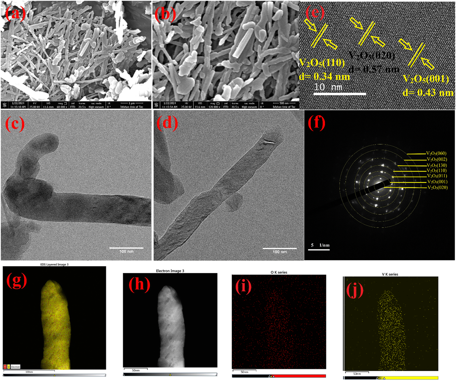 | ||
| Fig. 1 (a) and (b) Scanning electron microscopy (SEM) images at two different magnifications of V2O5 nanowires. (c) and (d) TEM and (e) HRTEM images and (f) SAED pattern of V2O5 NWs. The corresponding TEM/elemental mapping merged images (g and h) of the V2O5 nanowires, presenting the distribution of (i) O and (j) V elements. | ||
Fig. 2(a, b) and Fig. S1 (ESI†) show the FE-SEM images of the Te@PPy–V2O5 electrode with various tellurium photoelectrodeposition times in the range of 5.0–20 min. In addition, V2O5 nanowires are observed to be interconnected with PPy and a Te layer was deposited on the PPy–V2O5 substrate to form a rough and porous structure. As observed, increasing the Te photoelectrodeposition time of the PPy–V2O5 substrate from 5.0 to 20 minutes has decreased the porosity of the resulting electrode and the surface has become smooth. The cross-sectional images of the best photoelectrode (10 min. PE) are shown in Fig. S2 (ESI†). As the cross-sectional images clearly show, Te@PPy–V2O5 with 4.9 μm average thickness has been deposited on the flexible substrate. Fig. 2(c–f) shows the TEM and HRTEM images and SAED pattern of Te@PPy–V2O5. The morphology of the V2O5 nanowires has not been changed following photoelectrodeposition, which indicates that the procedure does not considerably affect the V2O5 morphology. The interplanar distances of 0.57, 0.43, and 0.34 nm are ascribed to (020), (001), and (110) lattice distances of orthorhombic V2O5, respectively. In addition, the interplanar distances of 0.31, 0.23, and 0.21 nm are due to the (101), (012), and (110) hexagonal phases of Te, respectively.43–49 The TEM mapping images of Te@PPy–V2O5 indicate the homogeneous distribution of Te, V, O, C, and N in the sample prepared (Fig. 2g–j). V and O come from V2O5, and N and C are due to PPy. Also the SEM image and related EDX mapping of the V2O5, PPy–V2O5 and Te@PPy–V2O5 are shown in Fig. S3–S5 (ESI†).
 | ||
| Fig. 2 (a) and (b) FESEM, (c) and (d) TEM, (e) high-resolution TEM image, (f) selected area electron diffraction (SAED) and (g)–(j) corresponding elemental mapping images of the Te@PPy–V2O5 sample. | ||
The crystalline structure and phase composition of the samples prepared were investigated by XRD (Fig. 3a). The broad diffraction peak at 2θ = 25° shows the amorphous nature of PPy resulting from the scattering from the PPy chains at the interplanar spacing. The peaks observed at 2θ = 28, 39, 41.5, 43.3, 51.4 and 64.2° are associated with (101), (012), (110), (200), (021), and (11−3) planes, respectively, and match the hexagonal phase of tellurium (JCPDS Card No. 01-085-0560). The reflection peaks observed at 2θ values of 15.2, 20.59, 25.9, 30.69, 32.3, 34.2, 41.4, 43, and 47° are due to the (020), (001), (110), (031), (101), (130), (002), (141), and (102) crystal planes, respectively, corresponding to the orthorhombic phase of V2O5 (JCPDS Card No. 01-085-0601). No other diffraction peaks are observed in the patterns of the V2O5 nanowire, indicating its good crystallinity and high purity. The chemical composition of the compounds and the chemical state of the elements were determined by XPS analysis. The high-resolution XPS analysis for the full range of the spectrum is shown in Fig. 3b. The survey spectrum shows the peaks associated with Te, V, In, Sn, N, O, and C. The corresponding calibration reference was the C 1s binding energy of 284.7 eV. The weak C peak is most probably associated with surface contamination occurring during sample handling and storage. The survey spectra for Te, Te@PPy, and Te@PPy–V2O5 on indium-doped tin oxide (ITO)-coated polyethylene terephthalate (PET) substrates are shown in Fig. 3b. In addition, the high-resolution peak scans for C 1s, N 1s, V 2p, O 1s, and Te 3d are shown in Fig. 3(c–g). In the high-resolution spectrum of V 2p (Fig. 3c), the most and least intense peaks appearing at 530.24 and 524.94 eV are ascribed to the O 1s and V 2p1/2, respectively. However, the other intense peak around 517 eV is due to V 2p3/2. The peaks of V 2p3/2 and V 2p1/2 are unsymmetrical shaped with a very weak shoulder line on the lower binding energy side. These peaks can be divided into V5+ and V4+ species, respectively, which indicates the generation of low valence state of vanadium.50 As Fig. 3d shows, the O1s spectrum is asymmetric and broad and may be deconvoluted into three peaks, indicating the presence of three various oxygen species. The peaks at 530.20, 531.40, and 533.0 eV are ascribed to the oxygens in V2O5, OH groups, and H2O molecules, respectively.51 The most intense peak in the C 1s spectrum at 284.7 eV is due to the α carbon atoms in the PPy ring (carbon atom bonded to a functional group) including C–C, C–H, or C![[double bond, length as m-dash]](https://www.rsc.org/images/entities/char_e001.gif) C (Fig. 3e). On the other hand, the component at 284.2 eV is linked to β carbon atoms. The component at 286.3 eV is due to the C–N bonds in the PPy structures, specifically the C–N+ bond of PPy polarons. Lastly, the peak with the smallest area, which appears at the highest binding energy (288.6 eV), corresponds to CO species.52 The N 1s peaks (Fig. 3f) are deconvoluted into three peaks at 401.55, 399.45, and 397.70 eV, which are ascribed to positive nitrogen atoms (NH+), a secondary amine-like structure (N–H), and an imine-like structure (CN) of the pyrrole ring, respectively.53 Finally, the peaks at 575 and 585.7 eV are ascribed to the Te 3d5/2 and Te 3d3/2, respectively, deposited on the PPy–V2O5/ITO electrode (Fig. 3g).
C (Fig. 3e). On the other hand, the component at 284.2 eV is linked to β carbon atoms. The component at 286.3 eV is due to the C–N bonds in the PPy structures, specifically the C–N+ bond of PPy polarons. Lastly, the peak with the smallest area, which appears at the highest binding energy (288.6 eV), corresponds to CO species.52 The N 1s peaks (Fig. 3f) are deconvoluted into three peaks at 401.55, 399.45, and 397.70 eV, which are ascribed to positive nitrogen atoms (NH+), a secondary amine-like structure (N–H), and an imine-like structure (CN) of the pyrrole ring, respectively.53 Finally, the peaks at 575 and 585.7 eV are ascribed to the Te 3d5/2 and Te 3d3/2, respectively, deposited on the PPy–V2O5/ITO electrode (Fig. 3g).
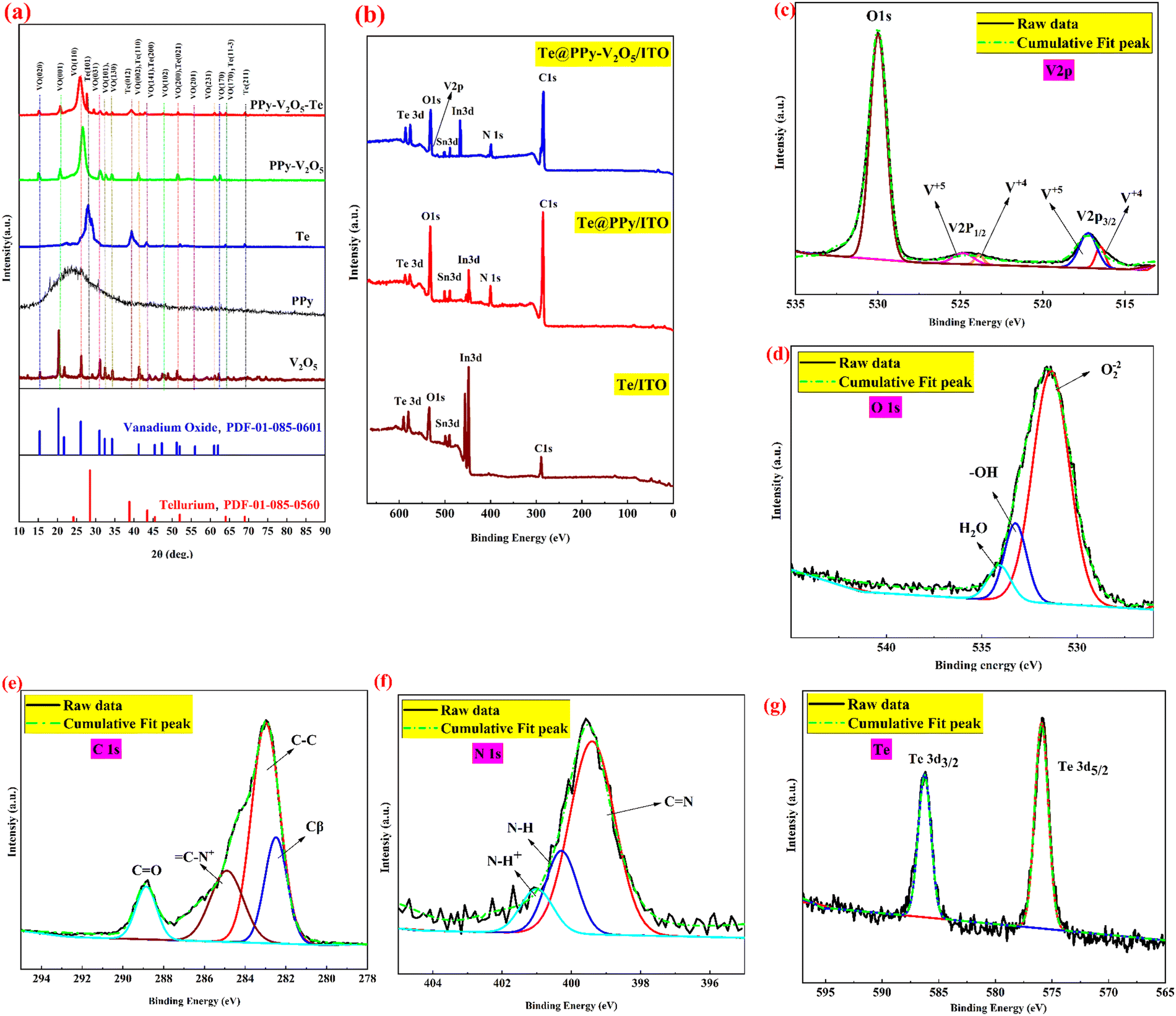 | ||
| Fig. 3 XRD and XPS plots of different samples: (a) XRD patterns of the V2O5, PPy, Te, PPy–V2O5 and Te@PPy–V2O5 electrodes. (b) XPS survey spectra of Te/ITO, Te@PPy/ITO and Te@PPy–V2O5/ITO. High-resolution XPS spectra of (c) V 2p peak, (d) O 1s peak, (e) C 1s peak, (f) N 1s peak and (g) Te 3d peak. | ||
Cyclic voltammetry (CV) and galvanostatic charge/discharge (GCD) analyses were performed using a standard three-electrode system to investigate the effect of deposition time and electrode preparation methods on the electrochemical performance of the prepared samples. The comparative GCD curves for the Te, V2O5, PPy, Te–V2O5, Te–PPy, and PPy–V2O5 electrodes at 2.0 mA cm−2 current density in the dark and under light illumination (Fig. 4(a, b) and Fig. S6, ESI†) indicate non-linear shapes similar to battery-like oxidation and reduction features. The discharge duration of PPy–V2O5 is the longest among all samples, indicating its excellent capacity. As observed, all the samples have longer charging/discharging times and therefore larger specific capacitance in the presence of light, which indicates the superior energy storage of these electrodes compared to those in the dark. PPy–V2O5 was selected as a light-sensitive substrate and various tellurium amounts were deposited on it. The electrochemical analysis of these electrodes was carried out in a 6.0 M LiCl electrolyte (as the optimized LiCl concentration; ESI,† Fig. S7 and S8) to study the effect of Te deposition time on the electrochemical activity of the Te@PPy–V2O5 electrodes obtained. The CV curves of different samples at a 60 mV s−1 scan rate are shown in Fig. 4(c and d). Maximum current response was shown by the sample (10 min. PE). The closed curve area associated with all samples is larger in the presence of light, which indicates the more area-specific capacitances of these samples. The CV curves of this electrode at voltage windows in the range of −0.8–0.3 V vs. Ag/AgCl in the dark and under light irradiation at the 60 mV s−1 scan rate are shown in Fig. 4e. The area of the CV curve under light irradiation is considerably larger, which indicates the higher specific capacity of this electrode. The changing trend of area-specific capacitance is shown in Fig. 4f. The CV measurement of the best electrode (sample 10 min. PE) was performed in the dark and under light irradiation at various scan rates in the 3.0–70 mV s−1 range in a three-electrode electrochemical configuration (Fig. 4g and Fig. S9, ESI†). The shape of the CV curves does not significantly change even at scan rates of over 70 mV s−1, which indicates the good energy storage properties of this electrode. Fig. 4h shows the specific capacitance values vs. scan rate for this sample under light irradiation and in the dark. In addition, based on our results, an inverse relationship exists between specific capacitance and scan rate. The specific capacitance at any scan rate is larger for light irradiation conditions. The cyclic voltammetry curves of this electrode with different voltage windows at 10 mV s−1 are shown in Fig. 4i and Fig. S10 (ESI†). The voltage window of this electrode can be extended to 0.7 V.
 | ||
| Fig. 4 GCD curves of Te, V2O5, PPy, Te–V2O5, Te–PPy and PPy–V2O5 electrodes at 2.0 mA cm−2 in 6 M LiCl electrolyte (a) in the dark and (b) under light conditions. CV curves of different Te@PPy–V2O5 electrodes at a scan rate of 60 mV s−1 (c) in the dark and (d) under light. (e) CV curves of the best sample in the dark and under light illumination. (f) Specific capacitance of different Te@PPy–V2O5 electrodes from the CD profile under both light and dark conditions. (g) CV curves of the best electrode at different scan rates in dark conditions. (h) Specific capacitance variation with the scan rate for the best electrode under both light and dark conditions. (i) CV curves of the best electrode with different working voltage windows at 10 mV s−1 in dark conditions. | ||
Fig. 5(a, b) and Fig. S11 (ESI†) show the charge–discharge plots of various Te@PPy–V2O5 samples at a 2.0 mA cm−2 current density in 6.0 M LiCl electrolyte under light irradiation and in the dark for 10 min. The PE sample has the largest discharge time from the GCD curve and highest specific capacitance, indicating its superiority compared with other Te@PPy–V2O5 electrodes. As observed, the discharge times are higher under light irradiation. First, the specific capacitance of the electrode is increased as the Te load increases, reaching the maximum at 10 min photo-electrodeposition. This may be due to an increase in the Te load on the PPy–V2O5 substrate, which could supply more active sites. Nevertheless, further increasing the time, reduces the specific capacitance of the electrode from 532 to 260 mF cm−2. Despite the increase in the amount of the deposited materials and film thickness, electrochemical reactions mostly take place at the active substance surface. The covered interior of the active substance is not capable of reacting with the electrolyte and contributing to the capacitance. The charge/discharge curves of this electrode at various current densities in the dark and under light irradiation are shown in Fig. 5(c and d). All curves are triangular with good linearity and small resistance drop, which indicates the outstanding supercapacitive behavior of this electrode. The GCD curves of this electrode at 3.1 mA cm−2 current density and voltage windows in the range from 0.9–1.3 V are shown in Fig. 5(e and f) and Fig. S12 (ESI†). The low internal resistance of this electrode in 6.0 M LiCl is further shown by the small IR drops of the GCD curves. Fig. 5f shows the GCD curve of the photoelectrode at different voltage ranges. This data confirms that the chosen operational voltage range of 0 to 1.0 V is optimal. At higher voltage potentials, the electrode exhibits significant ohmic drop, leading to suboptimal performance.
 | ||
| Fig. 5 GCD curves of different Te@PPy–V2O5 electrodes at a current density of 2.0 mA cm−2 (a) in the dark and (b) under light. GCD curves at different current densities for the best electrode (c) in the dark and (d) under light conditions. GCD profiles of the best electrode with various voltage windows at a current density of 3.1 mA cm−2 (e) in the dark and (f) under light. Comparison of the GCD curves for the best electrode under light and dark conditions at a 2.0 mA cm−2 current density (g). Specific capacitance of the best electrode versus current density based on the GCD curves (h) in the dark and (i) under light conditions. | ||
Impedance spectra were also recorded to further study the effect of Te deposition time on the electrochemical activity of the Te@PPy–V2O5 electrodes obtained. Nyquist plots were recorded in the 100 kHz–0.1 Hz frequency range at open circuit potential (Fig. 6a). Z′ and Z′′ correspond to the real and imaginary parts of the impedance. As shown, all Nyquist plots have the same shape, with two separate parts; that is, a linear part and a small semicircle arc in the low and high-frequency regions, respectively. The arc is usually associated with the charge transfer limiting process and is ascribed to the double-layer capacitance (Cdl) in parallel with the charge transfer resistance (Rct). The semicircle diameter is related to the charge transfer resistance, Rct, at the electrode and electrolyte interface as well as the resistance of the films of the paper. The inclined portion of the curve (about 45°) is due to the Warburg impedance, which represents ion diffusion in the electrolyte to the electrode surface. The Nyquist curve of the best electrode (10 min. PE sample) shows the smallest arc and most straight line among all the electrodes, indicating the low resistance and perfect capacitive performance of this electrode. EIS was carried out at open circuit potential to study the reaction kinetics of the photoelectrode in the dark and under light irradiation (Fig. 6b). Rs is identical in the presence and absence of light illumination. However, the charge transfer resistance (Rct) under light irradiation is smaller, implying that Te@PPy–V2O5 with superior photosensitivity can form a large number of photo-generated charge carriers to promote electrochemical reactions under light illumination. Mott–Schottky (M–S) plots were prepared at a 400 Hz frequency to investigate the effect of Te deposition time on the semiconducting properties of the Te@PPy–V2O5 electrodes fabricated. A positive slope in the linear region of the M–S plots is observed in all cases. This indicates the n-type behavior of these films. As shown in Fig. 6c, the flat band potential is found by the extrapolation of the curve to the x-axis in which the voltage at 1/C2 = 0 indicates the flat band potential. The electrochemical parameters of flat band potential and donor densities estimated for the samples prepared at different deposition times are shown in Table S2 (ESI†). As observed in Table S2 (ESI†), Te deposition on PPy–V2O5 has resulted in a slight shift towards more negative Efb values and an increase in the donor density (Nd). The 10 min PE electrode shows the highest Nd (1.85 × 1031 cm−3) among the eight Te@PPy–V2O5 electrodes prepared. This indicates that the optimum Te values can effectively enhance the carrier density. The photo charging and dark discharging of this electrode at different current densities and also the effect of photo charging time on the photovoltage and the discharge time are shown in Fig. 6d and e (also see ESI;† Fig. S13).
 | ||
| Fig. 6 (a) EIS of different Te@PPy–V2O5 electrodes. (b) Nyquist plots of the best electrode in the dark and under light illumination at open circuit potential. (c) Mott–Schottky plots of Te@PPy–V2O5 electrodes measured in the dark at a frequency of 1 kHz. (d) The photocharging and dark discharging of the best electrode at various current densities and (e) effect of photocharging time on the photovoltage and discharge time for the best electrode. | ||
The kinetic analysis was carried out to determine the mechanisms for the superior electrochemical performance of the Te@PPy–V2O5 electrode (see ESI;† Fig. S14 and S15). For the CV curves at different scan rates (at low scan rates) of this electrode, the relationship between the peak current (i) and scan rate (v) can be determined using the equation (i = avb), in which a and b are variable parameters. Specifically, the b-values of 0.5 and 1.0 indicate the diffusion-controlled and complete capacitive processes, respectively.54 As Fig. S14b (ESI†) shows, the anodic peak slope (b-value) is 0.51, which indicates the co-existence of the charge-storage mechanism of Te@PPy–V2O5 with the diffusion-control and capacitance processes. Thus, the above two contributions were investigated independently. According to Fig. S14c (ESI†), the capacitive process provides a smaller current response. Upon increasing the scan rate to 10 mV s−1, the capacitive process proportion increases from 19.71% to 27% (Fig. S14d, ESI†) due to the delayed availability of electrolytes to active sites. The capacitive contribution of this electrode is less than half of the total capacitance at these scan rates, which confirms the poor pseudocapacitive storage mechanism of the Te@PPy–V2O5 electrode. Nevertheless, as light is irradiated on the electrode surface, the Te@PPy–V2O5 electrode reaches a maximum capacitive contribution (Fig. S15, ESI†), which is considerably higher than that in the dark, which further confirms the improved pseudocapacitive storage mechanism of this electrode in 6.0 M LiCl electrolyte through light irradiation of the electrode.
A flexible solid-state photosupercapacitor (FSSPC) was prepared based on Te@PPy–V2O5 using LiCl/poly(vinyl alcohol) (PVA) gel electrolyte as the solid electrolyte to investigate the application of the pre-fabricated, independent flexible electrode (see ESI†). The electrochemical and photo-electrochemical energy storage behaviors of the photo-responsive supercapacitor prepared were studied using CV, charge/discharge, and cycling measurements. Fig. 7(a and b) show the CV curves of this supercapacitor, obtained at scan rates in the 5–100 mV s−1 range in the presence and absence of light. Redox peaks are observed in the CV curves of the as-prepared FSSPC, indicating that the PPy network on the FSSPC electrodes can still provide high pseudo capacitance. In addition, these two curves have different shapes, the curves with no illumination having sharp peaks, which appear as wider and broader peaks upon the exposure of the supercapacitor to light. The two CV curves, which combine faradaic and capacitive properties, remain stable upon constantly increasing the scan rate. This indicates a good rate of retention and fast current–voltage response. The areas of the CV curves are larger in the dark, indicating larger specific capacity upon light illumination (Fig. 7c). This FSSPC shows the maximum CV current of ∼166 μA cm−2 (in the dark) and the highest photo-electrochemical CV current of ∼250 μA cm−2. The plot of the comparison of the specific capacitance vs. scan rate is shown in Fig. 7d. The CV experiments of the FSSPC device fabricated were performed at 70 mV s−1 under different potential windows in the −1.2–0.8 and −1.2–1.2 V ranges in the absence and presence of light illumination, respectively (Fig. 7e and f) to evaluate the working potential window. As the potential increases to 1.2 V, no persistent redox peaks and polarization are observed.
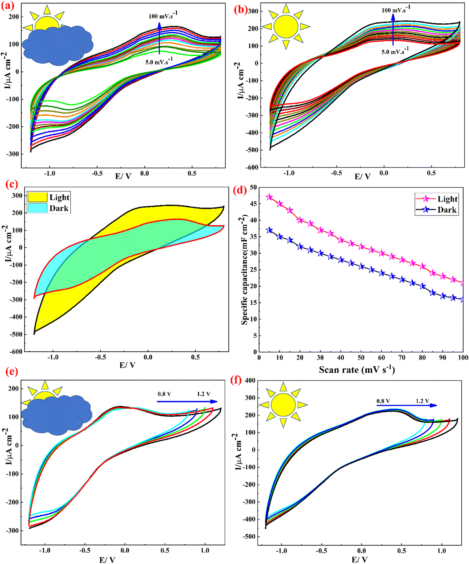 | ||
| Fig. 7 CV patterns of FSSPC at various scan rates (a) in the dark and (b) under light. (c) CV curves taken in the dark and under illumination of this device. (d) Specific capacitance variation with the scan rate for this FSSPC in the presence and absence of light. CV curves of this device at different potential windows (e) in the dark and (f) under light conditions. | ||
GCD measurements were carried out in various current densities in the range of 1.0–3.0 mA cm−2 in the presence and absence of light illumination to study the photo-electrochemical performance in detail. The approximately symmetrical triangular GCD diagrams obtained at different current densities (Fig. 8(a and b)) indicate superior capacitive behavior. In the dark, the areal-specific capacitance values of FSSPC are 46 and 20 mF cm−2 at current densities of 1.0 and 3.0 mA cm−2, respectively, indicating that the capacitance retention of FSSPC can still reach 64% as the current density is increased by three times. The GCD curves of this device in the presence and absence of light illumination are shown in Fig. 8c. The shape of the GCD curves is essentially the same as those in the absence of light irradiation, further indicating that no new electrochemical reaction occurs on light irradiation. Longer charge/discharge times are observed when the light is turned on, which indicates enhanced energy storage performance of the device by light irradiation. Switching the light source on increases the capacitance. At the current densities of 1.0, 1.2, 1.4, 1.6, 1.8, 2.0, 2.2, 2.4, 2.6, 2.8, and 3.0 mA cm−2, the specific capacitances in the absence of light are 46, 41, 37, 34, 31, 29, 27, 25, 23, 22, and 20 mF cm−2, respectively, while the corresponding values upon light irradiation are 131, 120, 112, 105, 100, 93, 79, 63, 57, 52, and 45 mF cm−2, respectively (Fig. 8d and e). Fig. 8f shows the charge–discharge curves of the FSSPC fabricated in different voltage ranges (also see ESI;† Fig. S16). As observed, the potential window of the GCD curves has increased from 2250 to 2750 mV. A wider voltage window of a supercapacitor can usually cause higher energy density. Nevertheless, more obvious polarization also causes lower electrochemical cycling stability. Thus, the electrochemical measurements of the FSSPC supercapacitor were performed at a voltage window of 2.2 V. To demonstrate the practical application of this FSSPC, relying on the ability of the fabricated device to harvest solar energy and deliver it in dark conditions (e.g. in cloudy conditions), the capability of photo charging this system and galvanostatically discharging it at different currents was shown. The photocharging of the device at a ∼2.0 V voltage when illuminated for 400 s and subsequent discharge in the dark at current densities of 0.7, 0.8, 0.9, and 1.0 mA cm−2 are shown in Fig. 8g (also see ESI;† Fig. S17, ESI†). Upon light illumination, the photoexcited electrons move from the photoelectrode to the counter electrode through the external circuit, which causes the adsorption of cations at the electrode–electrolyte interface to generate a double-layer at the interface. Nevertheless, anions are attracted towards the photoelectrode for adsorption at the electrode–electrolyte interface by the photogenerated holes (see Fig. S18, ESI†). The power and energy densities of the discharge were 702 W kg−1 and 78 W h kg−1, respectively, using the (0.73 A g−1) 0.7 mA cm−2 discharge curve. The power and energy densities for all the discharging currents have been shown in the ESI.†Fig. 8h shows the impact of light charging time on the resulting photovoltage and the discharge time of this FSSPC device. According to these results, this novel device can be charged in the presence of light without any external electrical source in addition to improving the photo-response in the electrochemical capacitance. Electrochemical impedance spectroscopy (EIS) was used to obtain the details of the interfacial processes, which occur in these FSSPC devices. Two clear features are observed in the EIS spectra of this device, recorded in the presence and absence of light illumination, a semicircle and an incomplete semicircle arc in the high and low-frequency regions, respectively (Fig. 8i). The presence of two semicircles shows that two processes are occurring. The low and high-frequency spectra correspond to the charge transport in the recombination phenomenon and the device, respectively, the former generally taking place at the interfaces.55 The capacitance of the FSSPC at low frequencies is caused by ion migration or dielectric charge accumulation phenomena. Such properties as huge dielectric constant or change in the magnitude of capacitance as light is illuminated are typical of semiconductors reported for some solar cells.55 The reduced low-frequency resistance of this device upon light illumination can be explained in the following manner: In the absence of light irradiation, a large electrostatic field is shown by the Te@PPy–V2O5 interface. Most charge carriers in the surface layer are remarkably increased by light irradiation, which leads to more free charge carriers and the interfacial electric field opposing the large electrostatic field. Apart from the effect of illumination on the properties of the device, the assignment of the low-frequency arc to the recombination or charge accumulation process is also supported by these conclusions. The Ragone plot of the Te@PPy–V2O5/ITO//Te@PPy–V2O5/ITO device was used to show the overall electrochemical properties of the assembled device (Fig. S19, ESI†). In the absence of light, the energy densities of the device at 1143, 1445, 1657, 1862, 1800, 2430, 2571, 2800, 3052, 3120, and 3150 W kg−1 power densities are 40, 34, 28, 22, 20, 18, 16, 14, 12, 11, and 10 W h kg−1, respectively. When the light is switched on, the energy density reaches 78, 66, 62, 58, 52, 46, 42, 36, 32, 24, and 18 W h kg−1 at power densities of 1135, 1400, 1636, 1884, 2102, 2341, 2585, 2793, 3012, 3265, and 3500 W kg−1, respectively, implying the enhancement of the energy density by light irradiation. The energy density of this assembled device is observed to be comparable to, or even higher than, that of many previously reported supercapacitors.
 | ||
| Fig. 8 Galvanostatic charge–discharge curves of FSSPC at different current densities (a) in the absence of light and (b) in the presence of light. (c) GCD curves of this device in the dark and under light, at a current density of 1.0 mA cm−2. The specific capacitance of the fabricated FSSPC at various current densities (d) with and (e) without light illumination. (f) GCD curves of this device at a current density of 2.8 mA cm−2 in different potential ranges. (g) Optical charging of the device and subsequent discharge in the dark at different current densities. (h) The effect of different times of light charging on the photovoltage and the discharge time of this FSSPC. (i) Electrochemical impedance spectra of this FSSPC measured at open circuit under different conditions. | ||
CV and GCD were studied under different bending angles to gain a more detailed understanding of the flexibility and mechanical stability of the FSSPC device. Fig. 9(a and b) show the CV curves at 80 mV s−1 with the bending angles of 0, 90, 180, and 360° in the presence and absence of light illumination. There are no significant differences among the CV curves obtained at different bending angles, which confirms the superior flexibility of this supercapacitor. The galvanostatic charge/discharge performances of the supercapacitor at different bending angles are shown in Fig. 9(c and d). These GCD curves also remain almost constant and indicate approximately symmetric triangular shapes at a 2.1 mA cm−2 current density. Importantly enough, the various bending angles applied on the device have almost no effect on its electromechanical performance, indicating its good mechanical flexibility. The electrode is stable against bending and strain as a result of the strong bonding between films and the ITO substrate. The long-term stability of the supercapacitor devices is a key factor in terms of their practical application and mechanical flexibility. Therefore, cycling tests were conducted for the flexible solid-state photosupercapacitor (FSSPC) in the presence and absence of light illumination (Fig. 9(e and f)). As observed, the initial specific capacitances delivered in the absence and presence of light irradiation are 37.8 and 23.2 mF cm−2, respectively, at a 3.2 mA cm−2 constant current density, whereas the capacitance retentions of 93 and 92.11% are obtained, respectively, after 12000 cycles. The slightly larger capacitance decay observed for the cycling under light irradiation can be due to the photocorrosion of electrode components. Nevertheless, a 35.4 mF cm−2 capacitance can still be delivered after 12000 cycles for the light-on case. This is still higher compared with the non-irradiated case (21.4 mF cm−2). The inset of these figures shows the changes in the charge and discharge curves of the first and last 3 cycles. Even though flexibility, reliability, and electrochemical performance are the principal performance indicators of FSSPC, they are all influenced by temperature. The majority of flexible SCs only operate at or near room temperature. However, the supercapacitors may be subject to such severe working conditions as low temperatures, high altitudes, and hot equatorial regions, which require temperature-resistant devices. The function of energy storage devices under different and severe conditions is very important with respect to their range of applications. Many researchers have already reported the operation of solid-state supercapacitors in wide ranges of temperature.56–61 For example, Rong et al. reported that organohydrogel electrolytes comprising PVA networks show flexibility and ionic conductivity even at temperatures below zero.62 In addition, Łatoszynska et al. have studied the capacitive behavior of the devices fabricated using gel polymer electrolytes with different solvent contents at the temperature range of −40 °C to 80 °C.63 According to the literature reports, performance is preserved in ionogel-based solid-state supercapacitors at temperatures over ambient. In this research, FSSPC showed a higher specific capacitance of 37 mF cm−2 at a current density of 2.4 mA cm−2 (1.19 times higher than that at ambient temperature), as shown in Fig. 9(g and h), arising from the higher electrochemical activity and faster ion transport of electrolyte ions at 50 °C. However, when the temperature is further increased, the specific capacitance starts to decrease for several reasons. From one aspect, the directional migration of ions in the electric field could be hindered by the excessively active motion of ions. Upon increasing the temperature, on the other hand, the charge transfer at the interface between the electrodes and the electrolyte becomes so hard that the decreased stability window of the electrolyte (i.e. the voltage drops) also reduces the specific capacitance. Nevertheless, the specific capacitance is still higher at high temperatures than that at ambient temperature (see ESI;† Fig. S20 and S21). The device still shows better rate capability at 50 °C compared with ambient temperature, but the rate capability decreases beyond this temperature. In addition, the device shows outstanding cycling stabilities with 89, 88, and 91% of the initial specific capacitance after 12000 charging/discharging cycles for these symmetrical supercapacitors at temperatures of −10 °C, 0 °C and 50 °C, respectively (Fig. S22 and S23, ESI†).
 | ||
| Fig. 9 CV curves of the fabricated flexible supercapacitor with bending angles of 0°, 90°, 180°, and 360° at a fixed scan rate of 80 mV s−1 (a) in the absence of light and (b) in the presence of light. GCD curves of this device at a current density of 2.1 mA cm−2 when bent to 0°, 90°, 180°, and 360° (c) in the dark and (d) under light. Cycling stability of the assembled FSSPC over 12000 cycles at 3.2 mA cm−2 (e) in dark and (f) light conditions (insets showing first and last 3 cycles at 3.2 mA cm−2). (g) Cyclic voltammograms of this device measured over a wide range of temperatures at −10 °C, 0 °C, 25 °C and 50 °C at a scan rate of 80 mV s−1. (h) GCD curves of this FSSPC at different temperature ranges from −10 °C to 50 °C at a current density of 2.4 mA cm−2. | ||
Considering the high demand for different applications, there has been significant research and development in the area of flexible and light supercapacitor devices. This FSSPC has been placed on a flower to show the light weight of the device fabricated (Fig. 10a). As observed, the device does not cause any bending in the flower. The excellent quality of the flexible ITO/PET electrode sheet is highlighted in Fig. 10b. A high optical transmittance is shown by this electrode. These properties make the electrode highly appropriate for optoelectronic applications. To study the practical application of the device, some small fans were powered by it. Having been charged by light irradiation (or solar light), the device can function as a power source for different electrical devices. Two FSSPC devices were woven into an individual fabric as the textile structure connection to fabricate the self-charging power textile. A tester wearing our designed self-charging power textile attached to a laboratory coat, which harvests light energy according to their daily outdoor and indoor activities, is shown in Fig. 10c (also see ESI;† Fig. S24). As can be observed, our flexible device can be directly sewn on a backpack. Therefore, this technology can be integrated into flexible, wearable fabrics in anything from suit jackets to tents to form a wearable fabric, which is capable of collecting enough solar power to keep small portable electronic devices completely charged. Contrary to some other commercial wearable solar technology, the solar charging in these novel textiles takes place at the fabric level and there would be no need for any traditional solar panel. These results indicate the potential application of this flexible FSSPC in ordinary wearable smart electronics.
 | ||
| Fig. 10 (a) Transparent and (b) light weight natures of fabricated FSSPC devices. (c) Demonstration of two FSSPC self-charging flexible devices directly sewn on a backpack and its operation. (d) and (e) Photograph of working some fans powered by the photographed FSSPC device under bending states. | ||
4. Conclusions
To sum up, an effective, light, and flexible photo-charging supercapacitor with high total system efficiency, and operational and mechanical stability has been prepared. A series of tellurium Te@PPy–V2O5 films have also been successfully prepared on flexible ITO substrates via electrodeposition and photo-electrodeposition techniques as photo-responsive supercapacitor electrodes with high specific capacitance and enhanced photo response. Upon illumination at a current density of 2.0 mA cm−2, the area-specific capacitance of the Te@PPy–V2O5/ITO electrode increases from 412 to 532 mF cm−2. The enhanced capacitance and outstanding photosensitivity of the Te@PPy–V2O5/ITO electrode are due to the synergism of components in its structures. Upon light illumination, the capacity of the flexible solid-state photosupercapacitor (FSSPC) fabricated using this electrode increased by 65%, according to GCD curves at constant current density (i = 1.0 mA cm−2), reaching its highest value of 130 mF cm−2. In addition, excellent cycling stability (up to 12000 cycles), and a minor change in areal capacitance to achieve a high coulombic efficiency of up to 93% for a current density of 10 mA cm−2, and applicability in flexible devices with outstanding capacitance retention of up to ∼90% in bending mode make this flexible photoresponsive, symmetrical supercapacitor an efficient, next-generation energy storage device. The supercapacitor also shows very good stability of specific capacitance at various operating temperatures. Consequently, this simple temperature-tolerant FSSPC device offers novel opportunities for a new generation of flexible energy storage devices under different harsh conditions. The FSSPC developed in this work shows outstanding mechanical flexibility and durability, allowing its application in future textile-based smart electronics daily. Such innovative development of solar energy storage devices takes advantage of the synergy of energy harvesting, storage, and utilization in one smart system and provides a possible solution for the fabrication of self-powered wearable electronics.
Data availability
The data used to support the findings of this study are included within the article.Conflicts of interest
There are no conflicts to declare.Acknowledgements
The authors wish to express their gratitude to the Research Affairs Division Isfahan University of Technology (IUT), Isfahan, for partial financial support.References
- M. Z. Iqbal and U. Aziz, J. Energy Storage, 2022, 46, 103823 CrossRef.
- J. Gong, C. Li and M. R. Wasielewski, Chem. Soc. Rev., 2019, 48, 1862–1864 RSC.
- R. Mittapally, A. Majumder, P. Reddy and E. Meyhofer, Phys. Rev. Appl., 2023, 19, 037002 CrossRef CAS.
- Q. Zeng, Y. Lai, L. Jiang, F. Liu, X. Hao, L. Wang and M. A. Green, Adv. Energy Mater., 2020, 10, 1903930 CrossRef CAS.
- J. Lee, K. Y. A. Lin, S. Jung and E. E. Kwon, Chem. Eng. J., 2023, 452, 139218 CrossRef CAS.
- L. Wang, L. Wen, Y. Tong, S. Wang, X. Hou, X. An, S. X. Dou and J. Liang, Carbon Energy, 2021, 3, 225–252 CrossRef CAS.
- E. Kabir, P. Kumar, S. Kumar, A. A. Adelodun and K. H. Kim, Renewable Sustainable Energy Rev., 2018, 82, 894–900 CrossRef.
- X. Gao, H. Wu, C. Su, C. Lu, Y. Dai, S. Zhao, X. Hu, F. Zhao, W. Zhang, I. P. Parkin, C. J. Carmalt and G. He, Energy Environ. Sci., 2023, 16, 1364–1383 RSC.
- S. Sharma and P. Chand, Results Phys., 2023, 5, 100885 CAS.
- A. A. Kebede, T. Kalogiannis, J. Van Mierlo and M. Berecibar, Renewable Sustainable Energy Rev., 2022, 159, 112213 CrossRef CAS.
- K. Namsheer and C. S. Rout, J. Mater. Chem. A, 2021, 9, 8248–8278 RSC.
- W. W. Tian, Y. D. Ying, J. T. Ren and Z. Y. Yuan, J. Mater. Chem. A, 2023, 11, 8024–8037 RSC.
- M. M. Momeni, A. Sharifi Renani and B. K. Lee, J. Alloys Compd., 2023, 962, 171204 CrossRef CAS.
- T. Li, W. Li, W. Long, H. Zhang, H. Tan, Y. Zhan and Z. Ren, J. Alloys Compd., 2024, 976, 173377 CrossRef CAS.
- A. Sharifi Renani, M. M. Momeni, H. Mohammadzadeh Aydisheh and B. K. Lee, J. Energy Storage, 2023, 62, 106866 CrossRef.
- J. Xu, H. Wu, L. Lu, S. F. Leung, D. Chen, X. Chen, Z. Fan, G. Shen and D. Li, Adv. Funct. Mater., 2013, 24, 1840–1846 CrossRef.
- Y. Ding, Z. Wang, X. Duan and R. Liu, Mater. Today Energy, 2023, 33, 101276 CrossRef.
- B. D. Boruah, A. Mathieson, B. Wen, C. Jo, F. Deschler and M. De Volder, Nano Lett., 2020, 20, 5967–5974 CrossRef CAS.
- M. Fu, R. Lv, Y. Lei and M. Terrones, Small, 2021, 17, 2004827 CrossRef CAS PubMed.
- M. F. El-Kady, V. Strong, S. Dubin and R. B. Kaner, Science, 2012, 335, 1326–1330 CrossRef CAS.
- J. Wu, X. Gao, H. Yu, T. Ding, Y. Yan, B. Yao, X. Yao, D. Chen, M. Liu and L. Huang, Adv. Funct. Mater., 2016, 26, 6114–6120 CrossRef CAS.
- X. Chen, L. Wang, H. Li, F. Cheng and J. Chen, J. Energy Chem., 2019, 38, 20–25 CrossRef.
- M. Lee, S. K. Balasingam, H. Y. Jeong, W. G. Hong, H. B. Lee, B. H. Kim and Y. Jun, Sci. Rep., 2015, 5, 08151 CrossRef CAS PubMed.
- Y. Lee and J. B. Goodenough, J. Solid State Chem., 1999, 148, 81–84 CrossRef.
- B. Saravanakumar, K. K. Purushothaman and G. Muralidharan, ACS Appl. Mater. Interfaces, 2012, 4, 4484–4490 CrossRef CAS.
- Y. Guo, J. Li, M. Chen and G. Gao, J. Power Sources, 2015, 273, 804–809 CrossRef CAS.
- S. D. Perera, A. D. Liyanage, N. Nijem, J. P. Ferraris, Y. J. Chabal and K. J. Balkus, J. Power Sources, 2013, 230, 130–137 CrossRef CAS.
- Q. Qu, Y. Zhu, X. Gao and Y. Wu, Adv. Energy Mater., 2012, 2, 950–955 CrossRef CAS.
- Y. Du, X. Wang, J. Man and J. Sun, Mater. Lett., 2020, 272, 127813 CrossRef CAS.
- T. Qian, N. Xu, J. Zhou, T. Yang, X. Liu, X. Shen, J. Liang and C. Yan, J. Mater. Chem. A, 2015, 3, 488–493 RSC.
- J. G. Wang, H. Liu, H. Liu, W. Hua and M. Shao, ACS Appl. Mater. Interfaces, 2018, 10, 18816–18823 CrossRef CAS.
- N. Jayababu, S. Jo, Y. Kim and D. Kim, ACS Appl. Mater. Interfaces, 2021, 13, 19938–19949 CrossRef CAS.
- H. P. Karki, H. Kim, J. Jung and J. Oh, Nanomaterials, 2021, 11, 2346 CrossRef CAS PubMed.
- R. Kowalik, D. Kutyła, K. Mech and P. Żabinski, Appl. Surf. Sci., 2016, 388, 817–824 CrossRef CAS.
- M. Manikandan, K. Subramani, S. Dhanuskodi and M. Sathish, Energy Fuel, 2021, 35, 12527–12537 CrossRef CAS.
- P. Bhol, S. Swain, S. Jena, K. Bhatte, C. S. Rout, M. Saxena, A. H. Jadhav and A. K. Samal, ACS Appl. Nano Mater., 2021, 4, 9008–9021 CrossRef CAS.
- C. K. Kim, J. M. Ji, M. Aftabuzzaman and H. K. Kim, RSC Adv., 2021, 11, 8628–8635 RSC.
- S. Manoharan, K. Krishnamoorthy, V. K. Mariappan, D. Kesavan and S. J. Kim, Chem. Eng. J., 2021, 421, 129548 CrossRef CAS.
- P. Bhol, S. Swain, S. Jena, K. Bhatte, C. S. Rout, M. Saxena, A. H. Jadhav and A. K. Samal, ACS Appl. Nano Mater., 2021, 4, 9008–9021 CrossRef CAS.
- H. Zhu, L. Fan, K. Wang, H. Liu, J. Zhang and S. Yan, Nanomaterials, 2023, 13, 2057 CrossRef CAS PubMed.
- S. Zhao, G. Tian, D. Zhang and Q. Wang, ACS Appl. Nano Mater., 2023, 6, 1849–1858 CrossRef CAS.
- P. Dutta, S. C. Karumuthil, R. Roy and A. K. Singh, ACS Appl. Polym. Mater., 2023, 5, 4088–4099 CrossRef CAS.
- H. B. Cho, H. J. Kim, N. S. Manikanta Viswanath, T. Samanta, J. W. Min, S. W. Jang, Y. M. Park, S. H. Jang, H. Yang and W. B. Im, J. Mater. Chem. C, 2024, 12, 3196–3202 RSC.
- M. B. Sreedhara, J. Ghatak, B. Bharath and C. N. R. Rao, ACS Appl. Mater. Interfaces, 2017, 9, 3178–3185 CrossRef CAS.
- I. J. Tadeo, R. Parasuraman, S. B. Krupanidhi and A. M. Umarji, Nano Express, 2020, 1, 010005 CrossRef.
- M. L. T. Ronquillo, P. S. Jacinto, P. Ovalle, L. R. Vázquez, E. C. Martínez, E. Marinero and V. Garibay, Mater. Sci. Appl., 2016, 7, 484 CAS.
- C. C. Wang, C. L. Lu, F. S. Shieu and H. C. Shih, Materials, 2021, 14, 359 CrossRef CAS PubMed.
- J. Zhou, G. Zhang, W. Wang, Q. Chen, W. Zhao, H. Liu, B. Zhao, Z. Ni and J. Lu, Nat. Commun., 2024, 15, 1435 CrossRef CAS PubMed.
- T. Kim, C. H. Choi, P. Byeon, M. Lee, A. Song, K. B. Chung, S. Han, S. Y. Chung, K. S. Park and J. K. Jeong, npj 2D Mater. Appl., 2022, 6, 4 CrossRef CAS.
- Z. Wang, L. Gao, S. Chen, L. Zhang and X. Yang, J. Solid State Electrochem., 2021, 25, 721–729 CrossRef CAS.
- Z. Li, Q. Zhu, S. Huang, S. Jiang, S. Lu, W. Chen and G. S. Zakharova, RSC Adv., 2014, 4, 46624–46630 RSC.
- M. Šetka, R. Calavia, L. Vojkůvka, E. Llobet, J. Drbohlavová and S. Vallejos, Sci. Rep., 2019, 9, 8465 CrossRef.
- X. Sun, X. Lv, M. Sui, X. Weng, X. Li and J. Wang, Materials, 2018, 11, 781 CrossRef.
- R. Barik, A. K. Yadav, S. N. Jha, D. Bhattacharyya and P. P. Ingole, ACS Appl. Mater. Interfaces, 2021, 13, 8102–8119 CrossRef CAS.
- P. Yadav, M. Hayal Alotaibi, N. Arora, M. Ibrahim Dar, S. M. Zakeeruddin and M. Grätzel, Adv. Funct. Mater., 2018, 1706073 CrossRef.
- A. A. Łatoszynska, P. L. Taberna, P. Simon and W. Wieczorek, Electrochim. Acta, 2017, 242, 31–37 CrossRef.
- A. Chaichi, G. Venugopalan, R. Devireddy, C. Arges and M. R. Gartia, ACS Appl. Energy Mater., 2020, 3, 5693–5704 CrossRef CAS.
- B. Asbani, C. Douard, T. Brousse and J. Le Bideau, Energy Storage Mater., 2019, 21, 439–445 CrossRef.
- Q. Rong, W. Lei, J. Huang and M. Liu, Adv. Energy Mater., 2018, 8, 1801967 CrossRef.
- J. Liu, Z. Khanam, S. Ahmed, H. Wang, T. Wang and S. Song, J. Power Sources, 2021, 488, 229461 CrossRef CAS.
- L. Negre, B. Daffos, V. Turq, P. L. Taberna and P. Simon, Electrochim. Acta, 2016, 206, 490–495 CrossRef CAS.
- Q. Rong, W. Lei, J. Huang and M. Liu, Adv. Energy Mater., 2018, 8, 1801967 CrossRef.
- A. A. Latoszynska, P. L. Taberna, P. Simon and W. Wieczorek, Electrochim. Acta, 2017, 242, 31–37 CrossRef CAS.
Footnote |
| † Electronic supplementary information (ESI) available. See DOI: https://doi.org/10.1039/d4tc03090g |
| This journal is © The Royal Society of Chemistry 2025 |