
 Open Access Article
 This Open Access Article is licensed under a
 Creative Commons Attribution 3.0 Unported Licence
Mobile intrinsic point defects for conductive neutral domain walls in LiNbO3†
Kristoffer
Eggestad
 ,
Benjamin A. D.
Williamson
,
Dennis
Meier
and
Sverre M.
Selbach
*
,
Benjamin A. D.
Williamson
,
Dennis
Meier
and
Sverre M.
Selbach
*
Department of Materials Science and Engineering, NTNU Norwegian University of Science and Technology, Trondheim, Norway. E-mail: selbach@ntnu.no
First published on 11th September 2024
Abstract
Conductive ferroelectric domain walls (DWs) hold great promise for neuromorphic nanoelectronics as they can contribute to realize multi-level diodes and nanoscale memristors. Point defects accumulating at DWs will change the local electrical transport properties. Hence, local, inter-switchable n- and p-type conductivity at DWs can be achieved through point defect population control. Here, we study the impact of point defects on the electronic structure at neutral domain walls in LiNbO3 by density functional theory (DFT). Segregation of Li and O vacancies was found to be energetically favourable at neutral DWs, implying that charge-compensating electrons or holes can give rise to n- or p-type conductivity. Changes in the electronic band gap and defect transition levels are discussed with respect to local property engineering, opening the pathway for reversible tuning between n- and p-type conduction at neutral ferroelectric DWs. Specifically, the high Curie temperature of LiNbO3 and the significant calculated mobility of O and Li vacancies suggest that thermal annealing and applied electric fields can be used experimentally to control point defect populations, and thus enable rewritable pn-junctions.
1 Introduction
Ferroelectric domain walls (DW) are natural interfaces between regions with uniform polarisation with a width at the unit cell level. Enhanced conduction at ferroelectric DWs was first demonstrated by spatially resolved conductance measurements of BiFeO3.1 While local changes in the band structure and band bending induced by DW bound charges2,3 were immediately recognized as important, it was also early realized that point defects play a crucial role for the transport behaviour of DWs.1,4–11Similar to the case of BiFeO3, point defects were associated with the emergence of DW conduction in various systems, especially at neutral DWs. For example, point defects at DWs in PbZrxTi1−xO3,12–14 h-RMnO315–20 and LiNbO3,21–26 are typically reported with reduced formation energies and often alter electronic transport, DW mobility and DW structure.
Ferroelectric LiNbO3 has been studied extensively for its DWs27–32 and more recently also because of hyperferroelectricity.33,34 The ground state structure is perovskite with space group R3c,35 and the measured spontaneous polarisation is ∼70 μC cm−2,36,37 and the TC ∼ 1200 °C.38 While the R3c structure allows 71°, 109° and 180° DWs,39 as observed in isostructural BiFeO3,40 the large distortion amplitude of LiNbO3 compared to aristotype cubic perovskite makes the coercive field for non-180° switching prohibitively large, rendering the material a uniaxial ferroelectric with only two accessible polar directions.41 Consequently, only two different neutral ferroelectric DWs are possible, commonly referred to as X- and Y-type DWs (Fig. S1, ESI†). The experimentally observed Y-type neutral DW is the most stable41 and thus the primary focus of this work.
DWs in LiNbO3 can display record-high conductivity ratio of 1012 higher than the surrounding domains.42 Seminal experiments demonstrated that the DWs enable non-volatile field-effect transistors,43 memory devices44,45 and memristors.42,46–48 Furthermore, integration of LiNbO3-based DW devices on silicon has been achieved,44,49,50 emphasizing the imminent application potential. However, the possibilities carried by point defects for emergent DW properties in LiNbO3 remains largely unexplored. As a perovskite with volatile Li occupying the A-site, both oxygen and lithium vacancies are expected to form. Finite concentrations of O or Li vacancies will be charge-compensated by electrons or holes, giving rise to n- and p-type conductivity, respectively.
Here, we study neutral 180° DWs in LiNbO3 using density functional theory (DFT) to calculate interactions between intrinsic point defects and DWs. Electronic structure along with the energetics and mobility of point defects are calculated and the possibility of reversibly tuning between n- and p-type conductivity at DWs is evaluated. Both Li and O vacancies are found to be relatively mobile and to prefer accumulation at neutral DWs, where they can reversibly induce p- and n-type conductivity, respectively. Finally, possible experimental realisation of this potential by thermal annealing and applied electric fields is discussed.
2 Results
2.1 Domain walls
We begin with the structure of neutral Y-type domain walls in LiNbO3. The calculated reference bulk properties presented in the ESI† agree with previous studies.35,37,51Y-type DWs have a lower calculated energy (141 mJ m−2) than X-type (158 mJ m−2), implying that Y-type DWs in the {xx0} planes are more stable41 (Fig. S1, ESI†), thus only Y-type DWs are studied here. For referense, DW energies reported for neutral 180° DWs in PbTiO3, BaTiO3, YMnO3 and YGaO3 of 132,52 7.552 and 1153 and 13–1554 mJ m−2, respectively, are all lower than for LiNbO3, following an expected correlation between polarisation magnitude and DW energy.6 In isostructural BiFeO3 a large DW energy of 829 mJ m−2 for 180° DWs has been reported,6 likely reflecting octahedral deformations and rotations across the DWs in BiFeO3,6 which are not observed across DWs in LiNbO3.
The calculated narrow DWs in LiNbO3, with bulk structure almost fully restored about 7 Å away, agree with previous DFT studies,55,56 and is expected from the high TC as the wall width is proportional to |T–TC|−1/2.57 Polarisation from a point charge model with formal charges, and Nb–O bond lengths, are displayed as a function of distance from a DW in Fig. 1(a) and (b), respectively. The deviation from bulk polarisation at the DWs diminishes abruptly and is almost gone about 4 Å from the DW. Across the DW, Nb ions shift their location within the Nb–O octahedra, as seen in Fig. 1(b), implying that three of the Nb–O bonds contract from more than 2.1 Å to less than 1.9 Å, and opposite for the remaining three Nb–O bonds in the octahedra.
 | ||
| Fig. 1 Structural parameters for a 160 atom Y-type DW cell as a function of distance from the domain wall. Panel (a) displays polarisation calculated using the point charge model, and panel (b) shows Nb–O bond lengths. The domain wall cell is displayed at the top with the DW marked by the solid black line, with oxygen atoms omitted for clarity. | ||
The layer-resolved electronic DOS across a DW is displayed in Fig. 2. The DOSes in the middle of the domains is very similar to that of bulk and the band gap is reduced by 0.41 eV at the DWs compared to bulk (ESI,† Fig. S3). As the structure approaches non-polar R![[3 with combining macron]](https://www.rsc.org/images/entities/char_0033_0304.gif) c structure at the DW, overlap between Op and Nbd (t2g) becomes less favourable, and valence band (VB) bonding states stabilised by second-order Jahn–Teller effect becomes less stable while anti-bonding states in the conduction band (CB) are shifted down in energy. The net result is a smaller band gap, with a larger contribution from CB minimum (CBM) lowering than raising of VB maximum (VBM).
c structure at the DW, overlap between Op and Nbd (t2g) becomes less favourable, and valence band (VB) bonding states stabilised by second-order Jahn–Teller effect becomes less stable while anti-bonding states in the conduction band (CB) are shifted down in energy. The net result is a smaller band gap, with a larger contribution from CB minimum (CBM) lowering than raising of VB maximum (VBM).
 | ||
| Fig. 2 Layer resolved electronic density of states for the 160 atom domain wall cell calculated using the PBEsol functional. The middle half of the domain wall cell is displayed to the right and aligned with the corresponding layers from which the DOS-es are extracted. | ||
The conduction band is significantly wider in energy at the DW than in bulk, but with no significant changes in band curvature (Fig. S7, ESI†). Degenerate bands at the CBM in the Γ-point in bulk become more localised at the DW, with the least curvy band being the one with the lowest energy. From these electronic structure features we can expect enhanced conductivity at the neutral Y-type DWs, with smaller band gap as the main contribution.
2.2 Point defects in bulk
Before examining point defects at DWs, we first examine the stability and mobility of common point defects in bulk LiNbO3. The thermodynamic transition level diagram, in Fig. 3, shows calculated defect formation energies, using the PBEsol functional, and chemical potentials resembling synthesis in air, as a function of the Fermi energy. The calculated stability region is displayed in ESI,† Fig. S10 and transition level diagrams for the edges of the stability region are shown in ESI,† Fig. S12. Defect formation energies do not change significantly with the HSE06 functional (ESI,† Fig. S13). The most important intrinsic defects in LiNbO3 are predicted to be NbLi, VLi and Lii throughout the entire stability window. The presence of NbLi and VLi are also reported from NMR experiments58 and DFT calculations.59,60 The formation energy of VO at the Fermi level is significantly higher than the previously mentioned defects, but it is also significantly lower than the rest of the defects investigated. The transition level diagrams in ESI,† Fig. S12 and S13 show relatively similar results for the different sets of chemical potentials except for the position of the Fermi level, which is located more than 1 eV from the band edges for the entire stability window.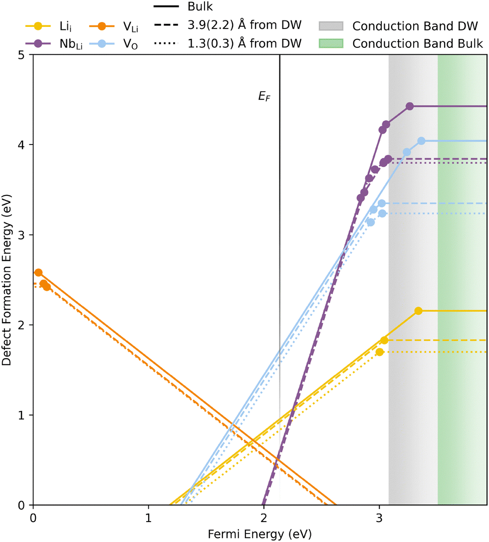 | ||
| Fig. 3 Thermodynamic transition levels for intrinsic defects, calculated for bulk (solid lines), close to (dashed lines) and at (dotted lines) a domain wall. The numbers in the parenthesis are the distances concerning the VO. Calculations were performed using PBEsol and the vertical faded black line is the calculated Fermi level. The defect formation energies are plotted as a function of the energy from the VBM to about 0.5 eV above the CBM of the bulk structure and calculated with mO = −2.0 eV and corresponding chemical potentials of Li and Nb. | ||
All transition levels are within the band gap, and most defects show either deep acceptor or donor behaviour. Calculations with PBEsol give a transition level of VLi close to the valence band maximum (VBM), but more than 1 eV into the band gap for the HSE06 calculations. A similar result is also displayed in the calculated electronic defect DOS-es, displayed in Fig. S9 (ESI†). PBEsol shows the charge compensating hole being in the valence band (VB) while the HSE06 calculations show the hole in the middle of the band gap. The partial charge densities of the unoccupied state resulting from PBEsol and HSE06 are displayed in ESI,† Fig. S14 and S15, respectively. The HSE06 calculations clearly result in the localisation of the hole while the hole in the PBEsol calculation is delocalised over several O ions. The HSE06 functional is known to more correctly localise holes and electrons,61,62 and should in principle give more correct results than PBEsol. In general, all transition levels found using the HSE06 functional lie deeper in the band gap than those found with PBEsol. As seen in the DOS plots in ESI,† Fig. S9, all defects investigated using HSE06 result in states localised well within the band gap.
From CI-NEB calculations, VLi and VO show migration barriers of ∼1.14 and ∼0.82 eV for both charged and neutral cells, respectively, as displayed in Fig. 4. DFT-calculated migration barriers of VO in perovskites are typically in the range of 0.5–0.9 eV.63–65 The migration barrier of VO in LiNbO3 falls in the higher end of this range, likely due to the high positive charge of Nb which is expected to impede the oxygen mobility. In Li solid-state electrolytes, reported migration barriers of VLi are often under 0.4 eV,66,67 considerably lower than the migration barrier calculated for LiNbO3 here, and than values reported in literature.68 In addition, the migration barrier of VLi, in LiNbO3, is substantially larger than the migration barrier of VO. This may be explained by the difference in interatomic distances; the O–O distance is ∼2.65 Å, while the Li–Li distance, of ∼3.78 Å, is significantly longer. Importantly, the calculated migration barriers are still sufficiently low to allow self-diffusion and field-migration of both VLi and VO below TC.
 | ||
| Fig. 4 Migration barriers for both neutral and charged VLi and VO in the LiNbO3 bulk structure. Energy, normalised to the initial structure, is plotted as a function of the distance moved by the defect. The charge of the charged cells including VLi and VO are −1 and +2, respectively. | ||
2.3 Point defects at Y-type domain walls
All point defects investigated show a propensity for accumulating at DWs, indicated by the lower lying dotted (at DW) and dashed (close to DW) lines in Fig. 3 (and ESI,† Fig. S18). The shaded grey and green areas indicate the conduction band at the DW and in bulk, respectively. VLi, VO and Lii show the lowest formation energy at the DW for all charge states. NbLi, in the +4 charge state, displays a lower formation energy at the second row from the DW, in agreement with previous work.25,69All donor defects are more shallow at the DW, but the transition level of the only acceptor defect investigated, VLi, is slightly deeper at the DW. VO shows the largest reduction in formation energy of −0.80 eV in neutral cells and the changes in defect formation energies from bulk are displayed in Table 1. The reduction in formation energy of donor defects in neutral cells calculated in this work is significantly larger than values reported for other oxides, e.g. ∼ 0.1,70 0.12,18 −0.02371 and −0.29971 eV for VO in h-LuFeO3, h-YMnO3, BaTiO3 and PbTiO3, respectively. Acceptor defects and defects in charge compensated cells show segregation energies closer to what is expected from strain fields associated with the domain walls,72 indicating that the reduced energy of the CBM significantly affects the formation energy of donor defects in neutral cells. LiNbO3 is thus a promising model system for the purpose of having mobile intrinsic donor and acceptor point defects which will accumulate at DWs in order to induce local n-type and p-type conductivity, respectively. The technological potential of such a model ferroelectric material is discussed further below.
| Energy difference (eV) | ||||
|---|---|---|---|---|
| 1.3 (0.3) Å | 3.9 (2.2) Å | |||
| Defect | Neutral | Charged | Neutral | Charged |
| VLi | −0.16 | −0.09 | −0.13 | −0.08 |
| Lii | −0.46 | −0.12 | −0.33 | −0.03 |
| NbLi | −0.63 | 0.00 | −0.58 | −0.06 |
| VO | −0.80 | −0.15 | −0.69 | −0.06 |
2.4 Domain wall mobility
DW migration barriers calculated in the absence and presence of point defects, displayed in Fig. 5, show that NbLi will result in strong DW pinning, in agreement with Lee et al.73 Furthermore, the presence of VLi and VO changes the migration barriers compared to the pristine structure. Locally, these migration barriers do not increase significantly compared to the calculated value from the pristine cell, although a global minimum in energy is found when the defects are close to the DW, reflecting their mutual affinity. Surprisingly, the local energy barrier for DW migration is not increased by VLi and VO, implying that a thermodynamic driving force for segregation at a DW does not necessarily imply strong pinning by a point defect. Considering the DW energy in ESI,† Fig. S1(b), the energy required to move the Y-type DW (34.6 mJ m−2), in the pristine cell, is about 1/4 of the energy needed to form the DW. With a NbLi defect in the cell, the energy needed to move the DW past the defect exceeds the energy required to form the DW. Migration barriers reported for neutral 180° DWs for h-YMnO3 and PbTiO3 of ∼3053,74 and 37 mJ m−2![[thin space (1/6-em)]](https://www.rsc.org/images/entities/char_2009.gif) 52 are of similar magnitude to our calculated values for pristine LiNbO3. Far away from the point defect, the DW migration barriers for the charged defect cells closely resembles the DW migration barrier of the pristine cell. This is also true for neutral VLi, but not for the donor defects, indicating that even larger cells would have been needed in order to properly restore bulk values. For comparison with the segregation energies, the migration barriers are also plotted in eV in Fig. S19 (ESI†).
52 are of similar magnitude to our calculated values for pristine LiNbO3. Far away from the point defect, the DW migration barriers for the charged defect cells closely resembles the DW migration barrier of the pristine cell. This is also true for neutral VLi, but not for the donor defects, indicating that even larger cells would have been needed in order to properly restore bulk values. For comparison with the segregation energies, the migration barriers are also plotted in eV in Fig. S19 (ESI†).
 | ||
| Fig. 5 Domain wall migration barriers with and without a point defect in the domain wall cell. The top panel shows a domain wall moving four times without any defects in the cell. The three other panels show similar DW movement, but with a single VLi, NbLi or VO in the cell, respectively. The position of the point defects is marked by the filled circles. The planar defect density is ∼0.012 Å−2 or 0.25 per formula unit. | ||
3 Discussion
The reduced band gap at the DWs increases the probability of charge carrier excitation across the band gap, and thus increased local conductivity can be expected from a higher local charge carrier concentration. Accumulation of VO and VLi also creates an electrostatic driving force for accumulation of charge-compensating electrons and holes, respectively, even if the deep defect state positions within the band gap are not optimal for electron or hole accumulation. The effective masses of electrons and holes, inferred from the curvature of the conduction and valence bands, respectively, do not change significantly at DWs compared to bulk. Reduced band degeneracy and lowering in the energy of the flat band at the CBM indicate subtly reduced mobility of electrons, hence enhanced n-type conductivity at DWs must rely on a sufficient increase in local electron concentration in the conduction band to compensate the lower mobility.Compared to the present study of neutral Y-type DWs, the band gap reduction at charged head-to-head (HH) and tail-to-tail (TT) DWs in LiNbO3 of ∼1.5 eV is much larger.75 Additionally, a significant increase in band curvature was also found at the DWs, explaining why DWs with an inclination angle, and thus also some HH character, show a greater conductivity than what we can predict in this study for neutral DWs.
As a result of the reduced CBM, a significant reduction in defect formation energies of neutral donor defects is observed at the DW, displayed in Fig. 3, thus shifting the transition levels towards the middle of the band gap. Comparing this change to the reduction of the CBM, all donor defects investigated show a more shallow transition level at the DW than in bulk. As a result, the probability of excitation of electrons from the n-type defects states to the conduction band, is enhanced at the DW. However, the predicted transition levels are still not ideally situated within the band gap for maximizing the DW conductivity, but nevertheless we can foresee a significant ratio in DW to bulk conductivity. As the VBM does not change at the DW, no large change in defect formation energy is observed for neutral VLi. The transition level of this defect is, as previously stated, slightly deeper at the DW, but this may be an artefact of PBEsol not easily localising the hole on O 2p, and more so in bulk than at the domain wall. With this in mind, the transition level in bulk should be slightly deeper than what we calculate and very similar to the transition level at the DW.
In bulk, VLi, NbLi and Lii, followed by VO have been shown to be the defects with the lowest formation energies. Due to expected Li loss during synthesis, Lii are not expected to be found to any large extent in experiments. The formation energy of VO is relatively high compared to the other defects, but carefully annealing LiNbO3 in H2-containing atmosphere should result in the formation of a finite concentration of VO. Higher temperature and pO2 will favour VO formation because of entropy and le Chatelier's principle, respectively. Unlike VLi and NbLi, VO formation is fully reversible by low temperature annealing in high pO2. Point defect formation energies are lower at DWs than in bulk, reflecting that the local DW structure is different from bulk. As point defects, like DWs, distort the local structure, accumulation of point defects at DWs maximizes the total volume of unperturbed bulk material in the system, thus minimizing the total energy.17,74
Based on the calculated migration barriers for VLi and VO we expect them to be mobile in an applied external electric field. However, a migration barrier of 0.82 eV for VO is relatively large and implies negligible self-diffusion at room temperature. Hence, annealing is likely necessary to enable sufficient point defect mobility to allow the energetically favourable accumulation to take place on a reasonable time scale. Note that the high TC of ∼1200 °C implies that the strain fields surrounding neutral DWs survive to sufficiently high temperatures to allow self-diffusion of VLi and VO, and thus also their segregation to DWs. Applied electric fields can in principle drive accumulation or depletion of point defects e.g. where a scanning probe microscopy (SPM) tip is applied. Any field-induced accumulation or depletion can in turn be progressively reversed by annealing at progressively higher temperatures as configurational entropy will favour an even spatial distribution of point defects. Naturally, the DWs themselves are more mobile than the point defects, and can thus be moved by lower applied electric fields than those necessary for accumulating or depleting a local region of point defects. Herein lies an unexplored potential for reversibly engineering local properties by SPM, in analogy with our previous work on writing conducting regions by electric field-induced anti-Frenkel defects in h-RMnO3.76
We stress that the presence of mobile intrinsic point defects of opposite charge is not restricted to VLi and VO in LiNbO3. For oxides, VPb in PbTiO3, and VBi in BiFeO3, are expected to be reasonably mobile cation vacancies with negative relative charge. Furthermore, point defects are generally more mobile in halide perovskites with larger ions with smaller formal charges,77 hence ABX3 halide perovskite where A is an alkali metal cation and X is a halide anion should in principle also show promise for engineering DW functionality by accumulation of mobile intrinsic point defects. An open question is how the inherent electric field from ferroelectric polarisation will affect the point defect distributions as both elastic fields from neutral DWs and electric fields from polarisation will benefit from screening by vacancies.
Our results, predicting relatively poor conductivity of neutral DWs, agree with experimental observations.27,28 However, as we see a trend of shallower defect levels of n-type defects with decreasing energy of the CBM together with the fact that head-to-head DWs show drastically reduced energy of the CBM,75 one should in principle be able to make slightly inclined DWs where n-type conductivity easily can be tuned by altering the VO concentration at the DWs with an external electric field. Furthermore, experimentally neutral DWs created by poling often result in slightly inclined DWs.78
Investigations of DW mobility reveal NbLi acting as pinning points for Y-type DWs, and thus with an increasing concentration of NbLi an increased coercive field is expected. This interaction can easily be explained by the very low mobility of Nb ions in the structure. As the DW moves, Li ions move a notable distance, while Nb and O ions do not. The presence of NbLi requires a comparatively immobile Nb ion to move the same distance as the Li ions, thereby increasing the barrier for DW migration. Apart from the reduced defect formation energies at the DWs, VLi and VO do not cause any additional pinning of the DWs.
To summarise, both VLi and VO are predicted to be mobile under applied electric fields at ambient temperature, in principle enabling manipulation of local point defect populations. Furthermore, both VLi and VO are predicted to accumulate at neutral ferroelectric DWs and thus favour accumulation of holes and electrons, respectively. The significantly reduced band gap at DWs of about 0.41 eV also support the potential for making memristive p-type or n-type DWs in LiNbO3 as well as rewritable pn-junctions. However, it should be noted that the deep defect energy levels in the band gap are not ideal for enhancing the DW conductivity and applied electric fields are expected to be necessary to excite electrons and holes to give significant DW conduction.
4 Conclusion
All defects investigated display an affinity for Y-type DWs, due to the inherent strain fields associated with the DWs. Both VLi and VO have been shown to be relatively mobile in the bulk structure and thus an accumulation of defects at the DWs is possible through annealing. Furthermore, investigations of DW mobility have reviled that NbLi will act as strong pinning points, while VLi and VO will not.A significant reduction in the CBM and band gap at DWs is observed and explained by a reduced second-order Jahn–Teller effect due to the polarisation inversion over the DW. Moreover, the reduction in the CBM results in a drastic reduction in the formation energy of donor defects in neutral cells, and more shallow transition levels of these defects.
We propose that neutral Y-type DWs in LiNbO3 can in principle be made reversibly n- and p-type conducting as mobile positive and negative intrinsic point defects can accumulate at the DWs. This implies locally enhanced charge carrier concentrations and thus enhanced DW conductivity compared to bulk. However, the deep transition levels of both VLi and VO as well as the relatively flat band edges are not optimal for enhancing the electronic conductivity and model materials with smaller band gaps and shallower defect transition levels should be explored further for designing memristive DWs and rewritable pn-junctions at DWs.
5 Computational methods
Density functional theory (DFT) calculations have been performed with VASP79–81 using the projector-argument wave method (PAW)82 to describe interactions between cores and the following valence electrons (Li: (1s2, 2s1), Nb: (3s2, 3p6, 4s2, 4d3), O: (2s2, 2p4)). Both the PBEsol83 and HSE0684 were used for electronic structure and defect calculations for bulk LiNbO3, while only PBEsol was used for large DW supercells with hundreds of atoms because of the trade-off between accuracy and cost.61,62 A plane-wave energy cutoff of 700 eV was used for all calculations.First, an initial optimisation of lattice parameters, angles and atomic positions was performed on the primitive structure (10 atoms). A Γ-centred k-point mesh of 5 × 5 × 5 was used for the 10 atoms rhombohedral unit cell with geometry relaxations until the force on all atoms was less than 0.1 meV Å−1 with both PBEsol and HSE06. Electronic structure was only calculated for Y-type DWs where the band structure was unfolded using the Easyunfold script85 onto the primitive unit cell.86 Spontaneous polarisation was calculated using the point charge model with formal charges and Born effective charges (BEC) with both PBEsol and HSE06 as well as with the Berry phase method87 (ESI,† Fig. S2). BEC were calculated with density functional perturbation theory with PBEsol.
An X-type neutral DW cell was created using a 1 × 8 × 1 expansion of the conventional cell with two domains of 20.5 Å each. A Y-type DW cell was constructed by expanding a 20-atom cell (displayed in ESI,† Fig. S16) with the Y-type DW parallel to the a–b plane, with two domains of 20.5 Å each. Γ-Centred k-points meshes of 5 × 1 × 2 and 3 × 4 × 1 were used for the X- and Y-type DW cells, respectively, and the geometries were relaxed until all forces on the ions were less than 0.01 eV Å−1.
The mobility of Y-type DWs was studied in pristine well as in the presence of intrinsic point defects using the climbing image nudged elastic band method (ciNEB)88,89 method with 5 images. For DW mobility calculations, the Y-type DW parallel to the a–b plane was constructed by a 1 × 1 × 8 expansion of a 40-atom cell (ESI,† Fig. S17) and Γ-centred k-point meshes of 3 × 3 × 1 were used. The ciNEB calculations were relaxed until all forces were less 0.03 eV Å−1.
Defect calculations were performed with PBEsol and HSE06 on 120 and 80 atom supercells, respectively (ESI,† Fig. S8). Ions were relaxed until forces on all atoms were less than 0.01 eV Å−1 with Γ-centred k-points meshes of 3 × 3 × 2 and 2 × 2 × 2 for PBEsol and HSE06 calculations, respectively. Calculations of defects at and close to Y-type DWs were done with a 2 × 2 × 8 expansion of the 20-atom cell (ESI,† Fig. S16) and a Γ-centred k-points mesh of 2 × 2 × 1 with ions relaxed until the forces were less than 0.02 eV Å−1.
Defect formation energies were calculated using90
 | (1) |
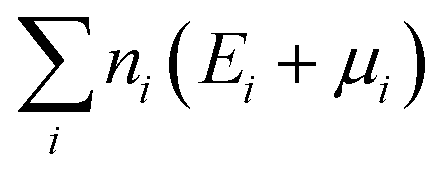 is the sum of the energies of elements removed from the structure, where ni, Ei and μi are the number, the reference energy and the chemical potential of element i. EF is the Fermi level, EVBM is the reference energy of the valence band maximum (VBM), and Epotcorr, EICcorr and EBFcorr are different types of correction schemes needed due to the finite supercell size. The potential alignment correction, Epotcorr, aligns the defect potential to that of the bulk, and the image charge correction, EICcorr, corrects for the long-range nature of Coulomb interactions,91 adapted for non-cubic cells.92 The band filling correction, EBFcorr, corrects for unphysical filling of electrons in the conduction band and holes in the valence band, respectively.91,93
The chemical potential limits analysis program (CPLAP)94 was used to find the thermodynamic stability regions of LiNbO3. The intermediate μO of −1.5 eV was chosen to reflect typical growth conditions for single crystals (1240 °C) using the Czochralski method. The Fermi level was determined self-consistently using the SC-FERMI script by Buckeridge,95 which uses charge neutrality and equilibrium defect concentrations. More details of the chemical potentials used and the Fermi level are provided in the ESI.†
The mobility of VLi and VO was studied using the ciNEB88,89 method with the 120-atom cell and PBEsol and 5 images and a spring constant of 5 eV−2 for both neutral and charged cells. Here, ions were relaxed until all forces on ions were less than 0.01 eV Å−1.
Author contributions
KE performed all the calculations and analysis related to this work with supervision from BADW and SMS. DM contributed to the reviewing, editing and supervision of the work. All authors contributed to the review and editing of the final manuscript and have given approval to the final version of the manuscript.Data availability
The conventional unit cell of LiNbO3 relaxed using DFT with the PBEsol and HSE06 functional and a X- and a Y-type domain wall cell relaxed using the PBEsol functional. Zipped folders contain relaxed structure files for defects in bulk, defect at Y-type domain walls, nudged elastic band (NEB) calculations of defects in bulk and NEB calculations of domain walls in the presence of defects.Conflicts of interest
There are no conflicts of interest in this work.Acknowledgements
The simulations were performed with resources provided by Sigma2 – the National Infrastructure for High-Performance Computing and Data Storage in Norway through project NN9264K. Support for this project was provided from the Research Council of Norway through projects 302506, 301954 and 275810. D. M. thanks NTNU for support through the Onsager Fellowship Program, the outstanding Academic Fellow Program, and acknowledges funding from the European Research Council (ERC) under the European Unions Horizon 2020 Research and Innovation Program (grant agreement no. 863691).Notes and references
- J. Seidel, L. W. Martin, Q. He, Q. Zhan, Y.-H. Chu, A. Rother, M. E. Hawkridge, P. Maksymovych, P. Yu, M. Gajek, N. Balke, S. V. Kalinin, S. Gemming, F. Wang, G. Catalan, J. F. Scott, N. A. Spaldin, J. Orenstein and R. Ramesh, Nat. Mater., 2009, 8, 229–234 CrossRef CAS PubMed.
- T. Sluka, A. K. Tagantsev, D. Damjanovic, M. Gureev and N. Setter, Nat. Commun., 2012, 3, 748 CrossRef PubMed.
- G. F. Nataf, M. Guennou, J. M. Gregg, D. Meier, J. Hlinka, E. K. H. Salje and J. Kreisel, Nat. Rev. Phys., 2020, 2, 634–648 CrossRef CAS.
- J. Seidel, P. Maksymovych, Y. Batra, A. Katan, S.-Y. Yang, Q. He, A. P. Baddorf, S. V. Kalinin, C.-H. Yang, J.-C. Yang, Y.-H. Chu, E. K. H. Salje, H. Wormeester, M. Salmeron and R. Ramesh, Phys. Rev. Lett., 2010, 105, 197603 CrossRef CAS PubMed.
- R. K. Vasudevan, A. N. Morozovska, E. A. Eliseev, J. Britson, J.-C. Yang, Y.-H. Chu, P. Maksymovych, L. Q. Chen, V. Nagarajan and S. V. Kalinin, Nano Lett., 2012, 12, 5524–5531 CrossRef CAS PubMed.
- A. Lubk, S. Gemming and N. A. Spaldin, Phys. Rev. B: Condens. Matter Mater. Phys., 2009, 80, 104110 CrossRef.
- T. Rojac, A. Bencan, G. Drazic, N. Sakamoto, H. Ursic, B. Jancar, G. Tavcar, M. Makarovic, J. Walker, B. Malic and D. Damjanovic, Nat. Mater., 2017, 16, 322–327 CrossRef CAS PubMed.
- D. Meier and S. M. Selbach, Nat. Rev. Mater., 2022, 7, 157–173 CrossRef CAS.
- P. Maksymovych, J. Seidel, Y. H. Chu, P. Wu, A. P. Baddorf, L.-Q. Chen, S. V. Kalinin and R. Ramesh, Nano Lett., 2011, 11, 1906–1912 CrossRef CAS PubMed.
- P. Sharma and J. Seidel, Neuromorphic Comput. Eng., 2023, 3, 022001 CrossRef.
- G. Catalan, J. Seidel, R. Ramesh and J. F. Scott, Rev. Mod. Phys., 2012, 84, 119–156 CrossRef CAS.
- I. Gaponenko, P. Tückmantel, J. Karthik, L. W. Martin and P. Paruch, Appl. Phys. Lett., 2015, 106, 162902 CrossRef.
- X. Wu and D. Vanderbilt, Phys. Rev. B: Condens. Matter Mater. Phys., 2006, 73, 020103 CrossRef.
- C.-L. Jia, S.-B. Mi, K. Urban, I. Vrejoiu, M. Alexe and D. Hesse, Nat. Mater., 2008, 7, 57–61 CrossRef CAS PubMed.
- T. S. Holstad, T. M. Ræder, D. M. Evans, D. R. Småbråten, S. Krohns, J. Schaab, Z. Yan, E. Bourret, A. T. J. van Helvoort, T. Grande, S. M. Selbach, J. C. Agar and D. Meier, npj Comput. Mater., 2020, 6, 163 CrossRef CAS.
- J. Schultheiß, J. Schaab, D. R. Småbråten, S. H. Skjærvø, E. Bourret, Z. Yan, S. M. Selbach and D. Meier, Appl. Phys. Lett., 2020, 116, 262903 CrossRef.
- J. Schaab, S. H. Skjærvø, S. Krohns, X. Dai, M. E. Holtz, A. Cano, M. Lilienblum, Z. Yan, E. Bourret, D. A. Muller, M. Fiebig, S. M. Selbach and D. Meier, Nat. Nanotechnol., 2018, 13, 1028–1034 CrossRef CAS PubMed.
- S. H. Skjærvø, D. R. Småbråten, N. A. Spaldin, T. Tybell and S. M. Selbach, Phys. Rev. B, 2018, 98, 184102 CrossRef.
- J. A. Mundy, J. Schaab, Y. Kumagai, A. Cano, M. Stengel, I. P. Krug, D. M. Gottlob, H. Doğanay, M. E. Holtz, R. Held, Z. Yan, E. Bourret, C. M. Schneider, D. G. Schlom, D. A. Muller, R. Ramesh, N. A. Spaldin and D. Meier, Nat. Mater., 2017, 16, 622–627 CrossRef CAS PubMed.
- D. R. Småbråten, Q. N. Meier, S. H. Skjærvø, K. Inzani, D. Meier and S. M. Selbach, Phys. Rev. Mater., 2018, 2, 114405 CrossRef.
- V. Gopalan, V. Dierolf and D. A. Scrymgeour, Annu. Rev. Mater. Res., 2007, 37, 449–489 CrossRef CAS.
- G. F. Nataf, M. Guennou, A. Haußmann, N. Barrett and J. Kreisel, Phys. Status Solidi RRL, 2016, 10, 222–226 CrossRef CAS.
- G. F. Nataf, O. Aktas, T. Granzow and E. K. H. Salje, J. Phys.: Condens. Matter, 2015, 28, 015901 CrossRef PubMed.
- D. Lee, H. Xu, V. Dierolf, V. Gopalan and S. R. Phillpot, Appl. Phys. Lett., 2011, 98, 092903 CrossRef.
- H. Xu, D. Lee, S. B. Sinnott, V. Gopalan, V. Dierolf and S. R. Phillpot, IOP Conf. Ser.: Mater. Sci. Eng., 2010, 15, 012003 Search PubMed.
- E. A. Eliseev, A. N. Morozovska, G. S. Svechnikov, V. Gopalan and V. Y. Shur, Phys. Rev. B: Condens. Matter Mater. Phys., 2011, 83, 235313 CrossRef.
- M. Schröder, A. Haußmann, A. Thiessen, E. Soergel, T. Woike and L. M. Eng, Adv. Funct. Mater., 2012, 22, 3936–3944 CrossRef.
- T. Kämpfe, P. Reichenbach, M. Schröder, A. Haußmann, L. M. Eng, T. Woike and E. Soergel, Phys. Rev. B: Condens. Matter Mater. Phys., 2014, 89, 035314 CrossRef.
- C. S. Werner, S. J. Herr, K. Buse, B. Sturman, E. Soergel, C. Razzaghi and I. Breunig, Sci. Rep., 2017, 7, 9862 CrossRef PubMed.
- M. Zahn, E. Beyreuther, I. Kiseleva, A. S. Lotfy, C. J. McCluskey, J. R. Maguire, A. Suna, M. Rüsing, J. M. Gregg and L. M. Eng, Phys. Rev. Appl., 2024, 21, 024007 CrossRef CAS.
- B. Kirbus, C. Godau, L. Wehmeier, H. Beccard, E. Beyreuther, A. Haußmann and L. M. Eng, ACS Appl. Nano Mater., 2019, 2, 5787–5794 CrossRef CAS.
- Y. Sheng, A. Best, H.-J. Butt, W. Krolikowski, A. Arie and K. Koynov, Opt. Express, 2010, 18, 16539–16545 CrossRef CAS PubMed.
- K. F. Garrity, K. M. Rabe and D. Vanderbilt, Phys. Rev. Lett., 2014, 112, 127601 CrossRef PubMed.
- P. Li, X. Ren, G.-C. Guo and L. He, Sci. Rep., 2016, 6, 34085 CrossRef CAS PubMed.
- S. Abrahams, J. Reddy and J. Bernstein, J. Phys. Chem. Solids, 1966, 27, 997–1012 CrossRef CAS.
- S. H. Wemple, M. DiDomenico and I. Camlibel, Appl. Phys. Lett., 1968, 12, 209–211 CrossRef CAS.
- W.-C. Yang, B. J. Rodriguez, A. Gruverman and R. J. Nemanich, Appl. Phys. Lett., 2004, 85, 2316–2318 CrossRef CAS.
- G. A. Smolenskii, N. N. Krainik, N. P. Khuchua, V. V. Zhdanova and I. E. Mylnikova, Phys. Status Solidi B, 1966, 13, 309–314 CrossRef CAS.
- S. K. Streiffer, C. B. Parker, A. E. Romanov, M. J. Lefevre, L. Zhao, J. S. Speck, W. Pompe, C. M. Foster and G. R. Bai, J. Appl. Phys., 1998, 83, 2742–2753 CrossRef CAS.
- F. Zavaliche, S. Y. Yang, T. Zhao, Y. H. Chu, M. P. Cruz, C. B. Eom and R. Ramesh, Phase Transitions, 2006, 79, 991–1017 CrossRef CAS.
- D. A. Scrymgeour, V. Gopalan, A. Itagi, A. Saxena and P. J. Swart, Phys. Rev. B: Condens. Matter Mater. Phys., 2005, 71, 184110 CrossRef.
- J. P. V. McConville, H. Lu, B. Wang, Y. Tan, C. Cochard, M. Conroy, K. Moore, A. Harvey, U. Bangert, L.-Q. Chen, A. Gruverman and J. M. Gregg, Adv. Funct. Mater., 2020, 30, 2000109 CrossRef CAS PubMed.
- X. Chai, J. Jiang, Q. Zhang, X. Hou, F. Meng, J. Wang, L. Gu, D. W. Zhang and A. Q. Jiang, Nat. Commun., 2020, 11, 2811 CrossRef CAS PubMed.
- A. Q. Jiang, W. P. Geng, P. Lv, J.-W. Hong, J. Jiang, C. Wang, X. J. Chai, J. W. Lian, Y. Zhang, R. Huang, D. W. Zhang, J. F. Scott and C. S. Hwang, Nat. Mater., 2020, 19, 1188–1194 CrossRef CAS PubMed.
- W. J. Zhang, B. W. Shen, H. C. Fan, D. Hu, A. Q. Jiang and J. Jiang, IEEE Electron Device Lett., 2023, 44, 420–423 CAS.
- D. B. Strukov, G. S. Snider, D. R. Stewart and R. S. Williams, Nature, 2008, 453, 80–83 CrossRef CAS PubMed.
- C. Godau, T. Kämpfe, A. Thiessen, L. M. Eng and A. Haußmann, ACS Nano, 2017, 11, 4816–4824 CrossRef CAS PubMed.
- H. Lu, Y. Tan, J. P. V. McConville, Z. Ahmadi, B. Wang, M. Conroy, K. Moore, U. Bangert, J. E. Shield, L.-Q. Chen, J. M. Gregg and A. Gruverman, Adv. Mater., 2019, 31, 1902890 CrossRef CAS PubMed.
- C. Wang, T. Wang, W. Zhang, J. Jiang, L. Chen and A. Jiang, Nano Res., 2022, 15, 3606–3613 CrossRef CAS.
- B. Shen, H. Sun, X. Hu, J. Sun, J. Jiang, Z. Zhang and A. Jiang, Adv. Funct. Mater., 2024, 2315954 CrossRef CAS.
- A. Savage, J. Appl. Phys., 1966, 37, 3071–3072 CrossRef CAS.
- B. Meyer and D. Vanderbilt, Phys. Rev. B: Condens. Matter Mater. Phys., 2002, 65, 104111 CrossRef.
- Y. Kumagai and N. A. Spaldin, Nat. Commun., 2013, 4, 1540 CrossRef PubMed.
- D. R. Småbråten, A. Nakata, D. Meier, T. Miyazaki and S. M. Selbach, Phys. Rev. B, 2020, 102, 144103 CrossRef.
- D. Lee, R. K. Behera, P. Wu, H. Xu, Y. L. Li, S. B. Sinnott, S. R. Phillpot, L. Q. Chen and V. Gopalan, Phys. Rev. B: Condens. Matter Mater. Phys., 2009, 80, 060102 CrossRef.
- D. Lee, H. Xu, V. Dierolf, V. Gopalan and S. R. Phillpot, Phys. Rev. B: Condens. Matter Mater. Phys., 2010, 82, 014104 CrossRef.
- E. K. Salje, Phase Transitions in Ferroelastic and Co-elastic Crystals, Cambridge University Press, 1991 Search PubMed.
- A. Yatsenko, E. Ivanova and N. Sergeev, Phys. B, 1997, 240, 254–262 CrossRef CAS.
- H. Xu, D. Lee, J. He, S. B. Sinnott, V. Gopalan, V. Dierolf and S. R. Phillpot, Phys. Rev. B: Condens. Matter Mater. Phys., 2008, 78, 174103 CrossRef.
- Y. Li, W. G. Schmidt and S. Sanna, Phys. Rev. B: Condens. Matter Mater. Phys., 2014, 89, 094111 CrossRef.
- B. G. Janesko, T. M. Henderson and G. E. Scuseria, Phys. Chem. Chem. Phys., 2009, 11, 443–454 RSC.
- A. J. Garza and G. E. Scuseria, J. Phys. Chem. Lett., 2016, 7, 4165–4170 CrossRef CAS PubMed.
- R. Rauschen and R. A. De Souza, Phys. Rev. Mater., 2022, 6, L111401 CrossRef CAS.
- T. Mizoguchi, N. Takahashi and H.-S. Lee, Appl. Phys. Lett., 2011, 98, 091909 CrossRef.
- S. V. Inge, A. Pandey, U. Ganguly and A. Bhattacharya, Phys. Rev. B, 2023, 108, 035114 CrossRef CAS.
- K. Meier, T. Laino and A. Curioni, J. Phys. Chem. C, 2014, 118, 6668–6679 CrossRef CAS.
- T. H. Wan and F. Ciucci, ACS Appl. Energy Mater., 2021, 4, 7930–7941 CrossRef CAS.
- C. Kofahl, L. Dörrer, B. Muscutt, S. Sanna, S. Hurskyy, U. Yakhnevych, Y. Suhak, H. Fritze, S. Ganschow and H. Schmidt, Phys. Rev. Mater., 2023, 7, 033403 CrossRef CAS.
- D. Lee, J. Korean Ceram. Soc., 2016, 53, 312–316 CrossRef CAS.
- P. Barrozo, D. R. SmÅbrÅten, Y.-L. Tang, B. Prasad, S. Saremi, R. Ozgur, V. Thakare, R. A. Steinhardt, M. E. Holtz, V. A. Stoica, L. W. Martin, D. G. Schlom, S. M. Selbach and R. Ramesh, Adv. Mater., 2020, 32, 2000508 CrossRef CAS PubMed.
- X. Y. Li, Q. Yang, J. X. Cao, L. Z. Sun, Q. X. Peng, Y. C. Zhou and R. X. Zhang, J. Phys. Chem. C, 2018, 122, 3091–3100 CrossRef CAS.
- X. He, S. Li, X. Ding, J. Sun, S. M. Selbach and E. K. Salje, Acta Mater., 2019, 178, 26–35 CrossRef CAS.
- D. Lee, V. Gopalan and S. R. Phillpot, Appl. Phys. Lett., 2016, 109, 082905 CrossRef.
- D. R. Småbråten, T. S. Holstad, D. M. Evans, Z. Yan, E. Bourret, D. Meier and S. M. Selbach, Phys. Rev. Res., 2020, 2, 033159 CrossRef.
- S. Liu and R. E. Cohen, J. Phys.: Condens. Matter, 2017, 29, 244003 CrossRef CAS PubMed.
- D. M. Evans, T. S. Holstad, A. B. Mosberg, D. R. Småbråten, P. E. Vullum, A. L. Dadlani, K. Shapovalov, Z. Yan, E. Bourret, D. Gao, J. Akola, J. Torgersen, A. T. J. van Helvoort, S. M. Selbach and D. Meier, Nat. Mater., 2020, 19, 1195–1200 CrossRef CAS PubMed.
- C. Eames, J. M. Frost, P. R. F. Barnes, B. C. O'Regan, A. Walsh and M. S. Islam, Nat. Commun., 2015, 6, 7497 CrossRef CAS PubMed.
- V. Y. Shur, E. L. Rumyantsev, E. V. Nikolaeva and E. I. Shishkin, Appl. Phys. Lett., 2000, 77, 3636–3638 CrossRef CAS.
- G. Kresse and J. Hafner, Phys. Rev. B: Condens. Matter Mater. Phys., 1993, 47, 558–561 CrossRef CAS PubMed.
- G. Kresse and J. Furthmüller, Comput. Mater. Sci., 1996, 6, 15–50 CrossRef CAS.
- G. Kresse and J. Furthmüller, Phys. Rev. B: Condens. Matter Mater. Phys., 1996, 54, 11169–11186 CrossRef CAS PubMed.
- G. Kresse and D. Joubert, Phys. Rev. B: Condens. Matter Mater. Phys., 1999, 59, 1758–1775 CrossRef CAS.
- J. P. Perdew, A. Ruzsinszky, G. I. Csonka, O. A. Vydrov, G. E. Scuseria, L. A. Constantin, X. Zhou and K. Burke, Phys. Rev. Lett., 2008, 100, 136406 CrossRef PubMed.
- A. V. Krukau, O. A. Vydrov, A. F. Izmaylov and G. E. Scuseria, J. Chem. Phys., 2006, 125, 224106 CrossRef PubMed.
- B. Zhu, S. R. Kavanagh and D. Scanlon, Open Source Softw., 2024, 9, 5974 CrossRef.
- V. Popescu and A. Zunger, Phys. Rev. B: Condens. Matter Mater. Phys., 2012, 85, 085201 CrossRef.
- N. A. Spaldin, J. Solid State Chem., 2012, 195, 2–10 CrossRef CAS.
- G. Henkelman, B. P. Uberuaga and H. Jónsson, J. Chem. Phys., 2000, 113, 9901–9904 CrossRef CAS.
- G. Henkelman and H. Jónsson, J. Chem. Phys., 2000, 113, 9978–9985 CrossRef CAS.
- C. Freysoldt, B. Grabowski, T. Hickel, J. Neugebauer, G. Kresse, A. Janotti and C. G. Van de Walle, Rev. Mod. Phys., 2014, 86, 253–305 CrossRef.
- S. Lany and A. Zunger, Phys. Rev. B: Condens. Matter Mater. Phys., 2008, 78, 235104 CrossRef.
- S. T. Murphy and N. D. M. Hine, Phys. Rev. B: Condens. Matter Mater. Phys., 2013, 87, 094111 CrossRef.
- C. G. Van de Walle and J. Neugebauer, J. Appl. Phys., 2004, 95, 3851–3879 CrossRef CAS.
- J. Buckeridge, D. Scanlon, A. Walsh and C. Catlow, Comput. Phys. Commun., 2014, 185, 330–338 CrossRef CAS.
- J. Buckeridge, Comput. Phys. Commun., 2019, 244, 329–342 CrossRef CAS.
Footnote |
| † Electronic supplementary information (ESI) available. See DOI: https://doi.org/10.1039/d4tc02856b |
| This journal is © The Royal Society of Chemistry 2024 |