
Damage mitigation as a strategy to achieve high ferroelectricity and reliability in hafnia for random-access-memory†
Junghyeon
Hwang
a,
Hunbeom
Shin
a,
Chaeheon
Kim
a,
Jinho
Ahn
*b and
Sanghun
Jeon
 *a
*a
aSchool of Electrical Engineering, Korea Advanced Institute of Science and Technology, 291 Daehakro, Yuseong-gu, Daejeon 34141, Republic of Korea. E-mail: jeonsh@kaist.ac.kr
bDivision of Materials Science and Engineering, Hanyang University, Seoul, Korea. E-mail: jhahn@hanyang.ac.kr
First published on 2nd November 2024
Abstract
Ferroelectric materials, characterized by their polarization switching capabilities, have emerged as promising candidates for non-volatile memory applications due to their fast operation speeds, low switching energies, and remarkable scalability. Among these, hafnia-based ferroelectrics are particularly noted for their compatibility with complementary metal-oxide-semiconductor (CMOS) technology. However, the development of high-quality ferroelectricity in ultra-thin films, essential for low-voltage operations and high-density integrations, remains challenging. This study introduces a novel low-damage metallization process designed to fabricate ultra-thin (sub-5 nm) ferroelectric films exhibiting exceptional ferroelectric properties and reliability. The process, compatible with standard CMOS techniques, achieves a significant remnant polarization (Pr) of 40 µC cm−2 and low leakage currents, alongside enhanced retention characteristics. Crucially, it substantially mitigates the wake-up effect, often attributed to oxygen vacancy redistribution at the interface. Through comprehensive analyses utilizing electron energy loss spectroscopy (EELS), geometric phase analysis (GPA) and X-ray photoelectron spectroscopy (XPS), we demonstrate that our process effectively reduces oxygen vacancies and dislocations at the top interface of the ferroelectric film. The enhanced reliability of ferroelectric random-access memory (FeRAM), evidenced by improved sensing margins and consistency in ferroelectric properties, marks a substantial improvement over the conventional method. To precisely measure reliability characteristics, we propose a new retention model that considers charge screening over time. Moreover, circuit-level simulations via non-volatile memory simulator (NVSim) validate the process's integration potential with existing CMOS technologies, affirming its suitability for advanced, high-density memory configurations without compromising performance or energy efficiency. The findings from this study pave the way for broader applications of nanoscale high-quality dielectric thin films, extending beyond ferroelectric materials to various technological domains requiring advanced material solutions.
Introduction
Ferroelectric memory, leveraging polarization switching mechanisms, has long been esteemed as a robust candidate for non-volatile memory applications due to its non-volatility, rapid operation speed, low energy consumption, and outstanding scalability.1–5 Particularly, hafnia-based ferroelectrics have garnered extensive attention for their seamless compatibility with existing complementary metal-oxide-semiconductor (CMOS) technologies. Ferroelectric memory utilizes a stable polarization switching process, which contrasts with conventional resistive-based random access memories that rely on ion transport. This offers ferroelectric memory both exceptional stability and, theoretically, infinite endurance.6,7The integration of ferroelectric memories with CMOS technology—including devices such as ferroelectric field effect transistors (FeFETs),8–14 ferroelectric tunnel junctions (FTJs),15–20 and ferroelectric random-access memory (FeRAM)21–24—has been propelled by advances in hafnia-based ferroelectrics.25 Specifically, FeRAM, which substitutes the DRAM capacitor with a hafnia-based ferroelectric, utilizes readout circuits to detect switching currents triggered by changes in ferroelectric film polarization, a few nanometers in thickness. Its non-volatile nature significantly cuts down the refresh time needed, positioning hafnia-based FeRAM as a potential successor to DRAM by addressing its inherent limitations.26
However, the application of hafnia-based ferroelectrics in ultra-thin films required for low-voltage operation (2 V) and high-density integration faces substantial hurdles due to high coercive fields (>1 MV cm−1) necessitating thickness scaling below 5 nm.27 Although hafnia ferroelectric thin films as thin as 1 nm have been reported, these have only been demonstrated on the silicon substrate, which limits their practical application in FeRAM.19 Moreover, when scaled to less than 10 nm, hafnia ferroelectrics exhibit accelerated degradation of ferroelectric properties, complicating the achievement of sufficient sensing margins and increasing the depolarization field, thereby challenging the construction of reliable devices with ultra-thin ferroelectric films.28,29
To overcome these obstacles, recent innovations have been made in various technological facets, including electrode engineering,28,30 plasma treatment,31 interfacial layer engineering,32,33 and various annealing processes.34–37 Particularly, X. Lyu et al. reported ferroelectricity and anti-ferroelectricity in 4 nm and 4.5 nm thick HfZrO films, respectively.38 They used WN electrodes to stabilize ferroelectricity through interfacial engineering. At 4 nm thick HfZrO with Hf![[thin space (1/6-em)]](https://www.rsc.org/images/entities/char_2009.gif) :Zr = 1:1, a remnant polarization (Pr) value of 13.8 µC cm−2 was achieved and 4.5 nm thick HfZrO with Hf:Zr = 1:3, a saturated polarization (Ps) value of 28.1 µC cm−2 was achieved. However, the leakage current density of 4 nm-thick film was over 10−1 A cm−2, which is quite a large value to the minimum requirement for the DRAM capacitor technology (10−7 A cm−2 at 0.8 V). Also, the reliability characteristics and cycling effects of the films were not reported and the origin of the good ferroelectricity was not well understood. S. Oh et al. reported the 2Pr value of 42.5 µC cm−2 at 5 MV cm−1 field with 2.5 nm thick HfZrO film and Pt as a bottom electrode.39 They asserted that the orthorhombic phase could not occur because the dead layer increased leakage current and that Pt can successfully reduce the formation of the dead layer. Pt is not, however, compatible with the CMOS process, making it unsuitable for use in ferroelectrics based on hafnia, where CMOS compatibility is the main benefit. The majority of the research, including the ones mentioned above, places a strong emphasis on the Pr value and provides little attention to the study of reliability features.
:Zr = 1:1, a remnant polarization (Pr) value of 13.8 µC cm−2 was achieved and 4.5 nm thick HfZrO with Hf:Zr = 1:3, a saturated polarization (Ps) value of 28.1 µC cm−2 was achieved. However, the leakage current density of 4 nm-thick film was over 10−1 A cm−2, which is quite a large value to the minimum requirement for the DRAM capacitor technology (10−7 A cm−2 at 0.8 V). Also, the reliability characteristics and cycling effects of the films were not reported and the origin of the good ferroelectricity was not well understood. S. Oh et al. reported the 2Pr value of 42.5 µC cm−2 at 5 MV cm−1 field with 2.5 nm thick HfZrO film and Pt as a bottom electrode.39 They asserted that the orthorhombic phase could not occur because the dead layer increased leakage current and that Pt can successfully reduce the formation of the dead layer. Pt is not, however, compatible with the CMOS process, making it unsuitable for use in ferroelectrics based on hafnia, where CMOS compatibility is the main benefit. The majority of the research, including the ones mentioned above, places a strong emphasis on the Pr value and provides little attention to the study of reliability features.
Recently, Cheng et al. discovered that in the annular dark-field mode, a sophisticated imaging technique, using Cs-corrected scanning transmission electron microscopy, significant dead layers are formed at the boundary between the top electrode and HZO layer.40 The dead layer was mainly composed of the t-phase. Meanwhile, the formation energy of the t-phase is known to be lower than that of the o-phase and m-phase when the oxygen vacancy concentration is high, stabilizing the t-phase in environments with high oxygen vacancy concentrations.41,42 They proposed that a damaging effect occurs during the deposition of TiN layers, resulting in the formation of an t-phase interfacial layer.
In this article, we provide a low-damage top electrode metallization method that can fabricate ultra-thin (5 nm) ferroelectric films with superior reliability and ferroelectricity. The low-damage top electrode metallization method was implemented using an atomic layer deposition (ALD) process characterized by low electron temperatures and high plasma density, as measured by optical emission spectroscopy (OES). With an ultra-thin ferroelectric capacitor, we achieved a 2Pr value (40 µC cm−2), low leakage current, and excellent retention properties by a straightforward and CMOS-compatible technique. Also, we discovered a significant reduction in the wake-up effect brought on by the redistribution of defects at the interface. It shows that the low-damage metallization process can reduce the defects of the thin film by preventing damage to the ferroelectric film during top electrode deposition. The dislocation of the ferroelectric film was visualized with a high-resolution cross-sectional transmission electron microscopy (HR-TEM) with electron energy loss spectroscopy analysis (EELS) and geometric phase analysis (GPA). To accurately assess the effects of the interfacial layer on retention, we proposed a new retention model that incorporates the charge screening effect. This model has allowed us to simulate and analyze the short-time retention characteristics of ultra-thin ferroelectric films comprehensively. Ultimately, this study examines the feasibility of deploying ferroelectric capacitors fabricated through this innovative process in FeRAM applications.
Comparison between conventional and low-damage process
Among various deposition techniques, plasma-enhanced atomic layer deposition (PEALD) is employed in DRAM processes due to its superior process control at low temperatures, particularly for 3D structuring and ultra-thin films. However, the ions generated in plasma can introduce defects in the films, degrading the properties of the oxide. Additionally, high-energy plasma radicals lead to the formation of interfacial layers, impacting the electrical characteristics of dielectric thin films.43–45 We monitored the plasma conditions to minimize damage during top film deposition using OES.Fig. 1(a) displays the OES for Ar/NH3 plasma as a function of the NH3 gas flow rate, indicating the dissociation degree of NH plasma through the ratio of NH to Ar peaks. Enhanced dissociation of NH3 plasma facilitates the generation of ionized ammonium ions and free nitrogen atoms, essential for the activation of reactants and effective film deposition in the PEALD process. As shown in Fig. 1(b), increasing the NH3 flow enhances the density of NH3 molecules in the plasma, boosting the likelihood of molecular collisions and thus promoting dissociation. However, this also increases the probability of recombination reactions, reducing dissociation levels beyond an NH3 flow of 250 sccm. Fig. 1(c) demonstrates that the electron temperature, which is proportional to the emission ratio of Ar 750 nm (2p1–1s2) to Ar 812 nm (2p9–1s5), can be effectively measured. In this analysis, the specific emission wavelengths of 750 nm and 811 nm for argon were chosen for their predominant excitation mechanisms: the former primarily through collisions exciting argon from the ground state, and the latter via excitation of metastable argon atoms.46 These were utilized to derive measurements of electron temperature.
 | ||
| Fig. 1 Plasma analysis and electron temperature measurement in PEALD Process. (a) Optical emission spectroscopy (OES) profiles for Ar/NH3 plasma, illustrating the dissociation degree of NH plasma as a function of NH3 gas flow rate. The ratio of NH to Ar peaks indicates dissociation levels. (b) Relationship between NH3 flow rate and NH molecular density in plasma, highlighting the increase in molecular collisions and dissociation up to 250 sccm, beyond which recombination reactions reduce dissociation effectiveness. (c) Measurement of electron temperature, derived from the emission ratio of Ar at 750 nm (2p1–1s2) and 812 nm (2p9–1s5), demonstrating the primary excitation mechanisms—collisional excitation from the ground state and excitation of metastable states, respectively. (d) Correlation between the intensity of the Ar 750 nm emission line and plasma density, showing an inverse relationship with electron temperature. | ||
Fig. 1(d) illustrates that the intensity of the Ar 750 nm emission line, proportional to plasma density, reveals an inverse relationship between electron temperature and plasma density.47 High plasma density reduces the mean free path of electrons, increasing collision frequency and energy loss at higher densities, consequently reducing ion bombardment energy and minimizing film damage. We have compared devices fabricated under low damage conditions (150 W, 250 sccm) with those under conventional conditions (300 W, 250 sccm), demonstrating significant differences in electron temperature and plasma density.
Ferroelectric capacitors are essential for next-generation ferroelectric random-access memory (FeRAM) technologies, which require high polarization, minimal leakage currents, and the absence of ‘wake-up’ effects for enhanced reliability and power efficiency. To this end, we performed polarization–voltage (P–V) and current–voltage (I–V) measurements with bipolar cycling. The P–V characteristics of the metal–ferroelectric–metal (MFM) capacitors employing both conventional and low-damage metallization processes are depicted in Fig. 2(a). These capacitors were characterized by a driving voltage of 1.75 V and a frequency of 100 kHz. Initial measurements with the conventional metallization process displayed antiferroelectric-like behavior, transitioning to ferroelectric characteristics after the wake-up process. This behavior is detrimental to FeRAM applications due to the necessity of a wake-up procedure to ensure adequate sensing margins.
 | ||
| Fig. 2 Characterization of MFM capacitors under conventional and low-damage metallization processes. (a) Polarization–voltage (P–V) characteristics showing initial antiferroelectric-like behavior in capacitors with conventional metallization, which transitions to ferroelectric characteristics after the wake-up process, and superior initial remnant polarization in low-damage processed devices, highlighting minimal wake-up effects. The measurements were conducted at a driving voltage of 1.75 V and a frequency of 100 kHz. (b) Comparison of remnant polarization (Pr) values showing a 30% increase in Pr for conventional process devices post wake-up, contrasted with a 300% increase in Pr for devices using the low-damage process. (c) Current–voltage (I–V) leakage current analysis across the two processes, illustrating a reduction of leakage currents by at least two orders of magnitude in the low-damage process compared to the conventional process, especially in the negative bias region, which is indicative of improved electrode engineering and reduced defect-induced leakage. | ||
Contrastingly, the low-damage metallization processed device exhibited a superior initial remnant polarization (2Pr) of 40 µC cm−2, with minimal wake-up effects, thereby enhancing its suitability for FeRAM use. This approach not only preserved the high polarization values but also significantly reduced the extent of wake-up, a crucial factor for device stability and reliability. As illustrated in Fig. 2(b), the Pr in devices employing the conventional process increased by 30% relative to the initial value, whereas devices processed with the low-damage technique exhibited a threefold increase in Pr value.
Multiple mechanisms, including phase transitions, domain wall depinning, and ferroelastic switching, have been proposed to explain the wake-up effect in hafnia ferroelectric films.48 These effects are largely attributed to the redistribution of oxygen vacancies at the interface, which are typically considered defects and can elevate the leakage current. The comparative analysis of leakage currents, as shown in Fig. 2(c), demonstrated a reduction by at least two orders of magnitude in the low-damage process compared to the conventional method, particularly in the negative bias region. This significant reduction is likely influenced by top electrode engineering, given the identical conditions of the bottom electrode and thermal processing across the devices.
To investigate the interface properties of the device, we employed pulse switching measurements, a method important for the analysis of ferroelectric interfaces as underscored in preceding investigations.49 The measurements began with the application of a pulse of substantial magnitude (4 MV cm−1) directed to completely invert the ferroelectric polarization. This was followed by the application of pulses with varied magnitudes (ranging from 3 MV cm−1 to 4 MV cm−1) in the reverse direction to discern the ferroelectric interface properties through the switching current induced by these pulses, as per the polarization reversal theory.50 The switching current, Isw(t), as a function of time, t, is governed by the equation:
 | (1) |
 | (2) |
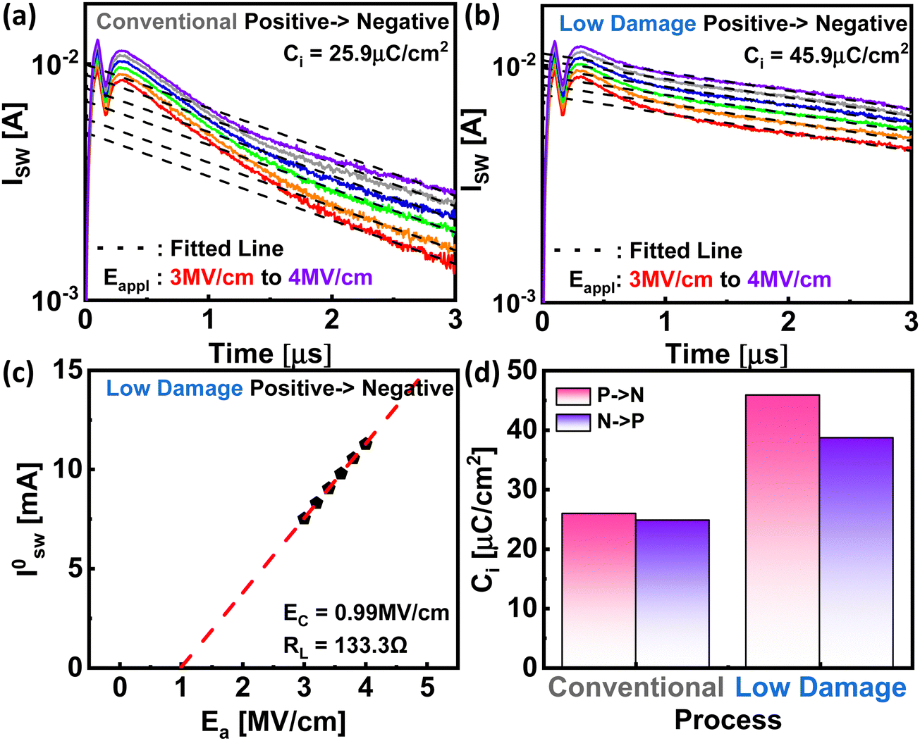 | ||
| Fig. 3 Pulse switching characteristics in ferroelectric capacitors. Transient domain switching currents Isw(t) for capacitors with (a) conventional and (b) low-damage processes, showing initial charging and discharging cycles followed by polarization switching. The low-damage process exhibits a more gradual current decay, indicating higher interfacial capacitance (Ci) and improved polarization retention. (c) Plot of initial polarization switching current (I0sw) versus applied field (Ea), used to deduce Ci. A steeper slope for the low-damage process suggests a thinner and more effective interfacial layer, leading to reduced operational voltage and enhanced retention stability. (d) Comparison of Ci values when using negative (pink) and positive (purple) read pulses, showing consistently higher Ci values in the low-damage processed device across both pulse types. | ||
Fig. 3(c) presents the relationship between I0sw and Ea, from which the Ci is deduced by evaluating the slope of the graph and x-axis intercept. When employing both a negative read pulse (pink) and a positive read pulse (purple), the low-damage processed device consistently demonstrated higher Ci values. (Fig. 3(d)) The pronounced slope associated with the polarization switching current suggests an enhancement in the interfacial capacitance for capacitors fabricated using the low-damage process, implying a comparatively thinner interfacial layer than that formed by conventional metallization. This interfacial layer, often a result of non-stoichiometric compound formation, becomes critically impactful with diminishing ferroelectric thickness, potentially leading to retention degradation and increased operational voltage.
Furthermore, pulse-switching characteristics were analyzed across wake-up cycles to ascertain the Ci value. Utilization of the low-damage process exhibited a stable Ci value up to 107 cycles, contrasting with the significant wake-up behavior seen in the conventional process (ESI,† Fig. S1). This observation aligns with the trend of increasing polarization with cycling as shown in Fig. 2, suggesting that defects within the interfacial layer, particularly oxygen vacancies, migrate or diffuse under field cycling, thereby restructuring the built-in field. The increase in Ci value is attributed to domain depinning or phase-transition-induced reduction of the dead layer. Beyond 107 cycles, a decrease in Ci values was observed in both samples, attributed to further defect generation. Milan Pešić et al. reported through simulations that field cycling in a TiN/HfO2/TiN stack MFM capacitor induces accelerated oxygen vacancy formation at the TiOx interface towards the electrode. These oxygen vacancy defects increase non-stoichiometric films at the interface, thereby diminishing the Ci value.
Unlike single-crystal ferroelectrics, which typically conform to the Kolmogorov–Avrami–Ishibashi (KAI) model,51 the switching behavior in polycrystalline hafnia-based ferroelectrics can be effectively modeled using the nucleation limited switching (NLS) approach.52,53 This model enables the analysis of domain sizes and defects within the ferroelectric layer.
Fig. 4(a) and (b) illustrate the ΔP(t)/2Ps values for MFM capacitors processed through conventional and low-damage processes, respectively. These graphs plot the change in polarization as a function of both the magnitude and width of the applied switching pulses, with detailed methodologies described in ESI,† Fig. S2. The device utilizing the low-damage process exhibits a pronounced, steep slope in the switching time versus the normalized polarization graph, suggesting a localized, concentrated switching event. Conversely, the device processed using conventional techniques shows a gentler slope, indicating a more dispersed polarization switching across the ferroelectric layer. This dispersion correlates with the slopes observed near the coercive field (Ec) in the P–E curve depicted in Fig. 1(a), further implying that multiple domains are simultaneously switched in the low-damage processed device compared to the conventional processed device.
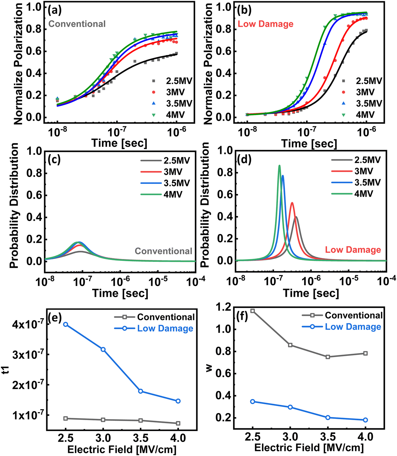 | ||
| Fig. 4 Analysis of polarization switching using the nucleation limited switching (NLS) model in polycrystalline hafnia-based ferroelectric devices. Polarization change (ΔP(t)/2Ps) as a function of switching pulse characteristics for MFM capacitors processed through (a) conventional and (b) low-damage processes. The steep slope in the low-damage device suggests localized, concentrated switching events, while the gentler slope in the conventional device indicates more dispersed domain switching. Lorentzian distribution functions corresponding to the fitted result for MFM capacitor with (c) conventional process and (d) low damage process demonstrating a sharply defined polarization distribution in the low-damage process compared to a broader, more gradual distribution in the conventional process. These patterns reflect the concentrated versus dispersed domain activities within the ferroelectric layer. (e) Extracted parameter t1, indicating the average domain nucleation time. Higher t1 values in the low-damage process suggest reduced disorder and fewer defects that promote early polarization switching, leading to improved device stability and performance. (f) Distribution of the domain size (w values) within the films, showing a narrower distribution indicating larger domain sizes in the low-damage process. Conversely, larger w values in the conventional process suggest smaller domain sizes and more restricted domain-wall propagation due to microstructural disorders. | ||
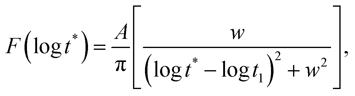
The fitting of polarization data to the NLS model is governed by the following equations:
 | (3) |
 | (4) |
t1 is the mean distribution value. This model captures the diverse nucleation times for each domain, offering a stark contrast to the more uniform switching mechanisms described by the KAI model for single crystals. The results, presented in Fig. 4(c) and (d), show a sharply defined distribution for the low-damage process, reinforcing the hypothesis that switching is highly localized. Conversely, a broader distribution observed in the conventional processed device indicates a more gradual and widespread domain switching.
The extracted parameter t1, displayed in Fig. 4(e), reveals an increased value in the device employing the low-damage process, suggesting a reduction in the disorder-induced local fields that typically promote early polarization switching under weaker electric fields.54 These local fields, arising from defects such as oxygen vacancies, interfacial imperfections, and domain boundaries, are mitigated in the low-damage process.
Furthermore, the parameter w from the distribution, depicted in Fig. 4(f), provides additional information about the domain size distribution within the films. A smaller w value denotes a narrower distribution of domain switching times, which correlates with larger domain sizes. Devices utilizing the conventional process exhibited larger w values, indicating smaller domain sizes and more restricted domain-wall propagation due to the aforementioned microstructural disorders. Conversely, the low-damage process, by minimizing these defects, supports the growth of larger and more uniformly distributed domains across the ferroelectric film. These findings underscore the critical role of film processing techniques in determining the microstructural and electrical properties of hafnia-based ferroelectric devices. By optimizing the processing conditions to reduce microstructural disorders, the low-damage process not only enhances the domain size but also promotes a more homogeneous domain distribution, crucial for the development of high-performance ferroelectric devices.
To investigate the leakage current characteristics attributed to defects, we conducted measurements of the current density–voltage (J–E) characteristics for MFM capacitors fabricated using both conventional and low-damage processes. These measurements spanned temperatures from 298 K to 358 K, in increments of 15 K, as shown in Fig. 5(a) and (b). In both sample sets, an increase in leakage current was observed with rising bias voltage and temperature, indicative of field-enhanced thermal emission of electrons. Remarkably, devices employing the low-damage process exhibited leakage currents approximately two orders of magnitude lower across all tested temperatures compared to their conventional counterparts.
 | ||
| Fig. 5 Leakage current analysis of MFM capacitors using the Poole–Frenkel emission model. Current density–voltage (J–E) characteristics of MFM capacitors at temperatures ranging from 298 K to 358 K for devices processed through (a) conventional and (b) low-damage processes, respectively. Graphs show an increase in leakage current with rising bias voltage and temperature, with the low-damage process devices exhibiting significantly lower leakage currents by approximately two orders of magnitude across all temperatures. Poole–Frenkel plots demonstrating the linear dependency of log(J/E) on the electric field (E) for both (c) conventional and (d) low-damage processed capacitors. These plots are used to analyze the thermally stimulated emission of electrons across the interface and within the dielectric. (e) and (f) Graphs depicting the variation of parameter b(T) as a function of q/kT, where b(T) is derived from the slope of the Poole–Frenkel plots and is used to calculate the barrier height Φt of the trap states. The results show barrier heights of 0.39 eV for conventional and 0.64 eV for low-damage processed devices, indicating deeper trap depths and reduced defect presence in the low-damage devices. | ||
The leakage mechanism was analyzed using the Poole–Frenkel emission model, which posits that thermally excited electrons from a metal layer transit into the dielectric without encountering significant energy barriers at the interface and are subsequently moderated by traps within the dielectric. The leakage current density, governed by this model, is expressed as:
 | (5) |
Fig. 5(c) and (d) display the Poole–Frenkel plots for the MFM capacitors processed via conventional and low-damage techniques, respectively. The characteristic linear dependency of log(J/E) on E confirms the Poole–Frenkel emission of the leakage current, described by:
 | (6) |
 | (7) |
 | (8) |
As depicted in Fig. 5(e) and (f), b(T) is plotted as a function of q/kT. Utilizing eqn (8), the barrier height Φt was derived from the slope of the b(T) versus q/kT plot. The fitting results indicated Φt values of 0.39 eV for devices processed using the conventional method and 0.64 eV for those using the low-damage process. The disparity in trap depths is attributed to the different defect profiles in these films, including oxygen vacancies, grain boundaries, and the presence of carbon, hydrogen, and nitrogen atoms, which can form traps. According to the Poole–Frenkel model, which favors the predominance of the shallowest trap, the low-damage process effectively minimizes the formation of such shallow traps, manifesting only deeper traps.
Origin of the excellent ferroelectricity of the low-damage process ferroelectric capacitor
In this investigation, a combination of X-ray diffraction (XRD), high-resolution transmission electron microscopy (HR-TEM), and X-ray photoelectron spectroscopy (XPS) depth profile analyses was employed to discern the physical mechanisms underpinning the superior performance of the ferroelectric capacitor fabricated using the low-damage process. The crystallographic diversity of HZO includes monoclinic (P21/c space group), tetragonal (P42/nmc space group), and orthorhombic (Pbca space group) phases. The ferroelectric behavior in polycrystalline HZO thin films is predominantly linked to the stabilization of the polar orthorhombic phase (Pca21), a finding supported by decades of extensive research. Grazing incidence X-ray diffraction (GIXRD) was utilized to examine the crystalline phases present (ESI,† Fig. S3). Notably, the GIXRD patterns at 2θ = 30.5° demonstrated the coexistence of the 110° phase—indicative of ferroelectricity—and the 101t phase, associated with a non-polar state. Although the intensity ratio of these phases can shift the peak positions, comparative analysis of the XRD spectra from the two samples showed no significant alterations at 30.5 degrees, indicating the stability of the crystal phases across different processing methods.Furthermore, to elucidate the impact of oxygen vacancies on the electrochemical properties of HZO thin films, electron energy loss spectroscopy (EELS) spectral imaging was conducted, specifically targeting the O K edge. Fig. 6(a) and (b) display the EELS spectra from the low-damage and conventional samples, respectively, captured vertically from the top to the bottom of the films as depicted in Fig. 6(c) and (d). The O K energy-loss near-edge structure (ELNES) in HZO is characterized by a double-peak profile, labeled a (around ∼534 eV) and b (∼538 eV), with peak a's intensity and sharpness being particularly sensitive to the crystallinity and oxygen vacancy content within the HfO2 matrix. Given that both sets of HZO films were subjected to identical thermal conditions, any deviations observed in the O K ELNES are primarily attributed to differences in oxygen vacancy concentrations or defects induced during the deposition of the top TiN layer.
 | ||
| Fig. 6 Characterization of oxygen vacancy distribution and microstructural quality in HZO thin films. Maps of the a/b ratio for HZO samples processed using (a) low-damage and (b) conventional processes, reconstructed through nonlinear least squares (NLLS) fitting of acquired EELS spectral imaging (SI) datasets. The low-damage process shows a non-uniform distribution with reduced oxygen vacancy concentrations towards the film's surface, suggesting effective control over defect generation during the deposition process. Average OK EELS spectrum of the HZO film area from the (c) low-damage process sample, and from (d) the conventional process sample. Colored rectangles in each map correspond to the colors used in the spectra graphs, indicating the location-specific spectral data. The color scale bar below indicates the range of measured a/b ratios at the OK edge. | ||
To quantitatively assess the presence of oxygen vacancies within these films, the relative intensities of peak a within the O K ELNES were analyzed using a nonlinear least squares (NLLS) method to calculate the b/a ratio across the film's profile.55 This b/a ratio acts as an indicator of oxygen vacancy content, where higher ratios indicate increased vacancy presence due to the relative reduction in peak a's intensity. Remarkably, the analysis revealed a significant decrease in the content of oxygen vacancies or defects in samples processed with minimized damage. Unlike the uniform distribution observed in conventional samples, a spatially non-uniform distribution of oxygen vacancies was identified in the low-damage samples, with vacancies preferentially aligning along the [00−1] crystallographic direction and exhibiting reduced concentrations toward the film's surface. These observations are corroborated by X-ray Photoelectron Spectroscopy (XPS) results, further substantiating the spatial variation in oxygen vacancy distribution within these engineered thin films (ESI,† Fig. S4). In addition, we employed scanning transmission electron microscopy (STEM) and geometric phase analysis (GPA) to compare the microstructural quality of ferroelectric films produced by low-damage and conventional metallization processes, observing that the low-damage process results in less strain and fewer dislocations (ESI,† Fig. S5).
Excellent reliability characteristics of the low-damage process ferroelectric capacitor
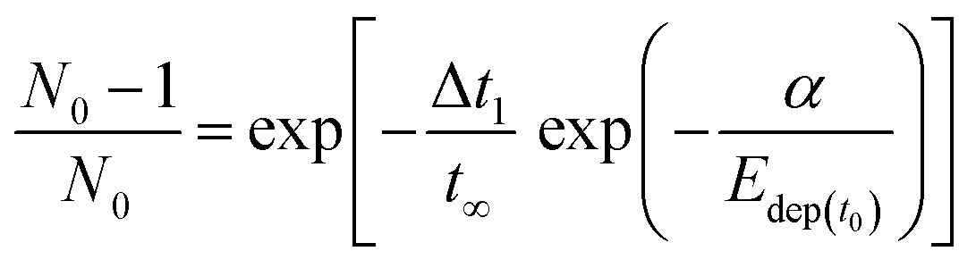
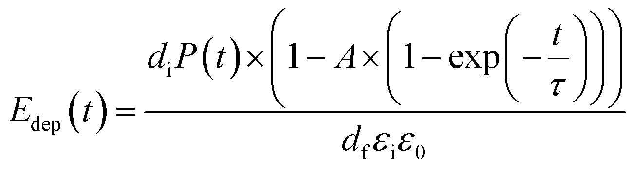
Retention challenges in ultra-thin ferroelectric films are considered a principal barrier to the widespread adoption of ferroelectric random access memory (FeRAM). It has been observed that a significant fraction of retention losses transpire within the initial sub-second period, with comparatively minor degradation occurring over longer durations (t > 1 s).56 The primary mechanism attributed to short-term polarization loss is the depolarization field, while long-term retention losses are predominantly associated with imprint phenomena.57 This description underscores the impact of depolarization within the first few seconds of retention loss. The mathematical expression for the depolarization field, | (9) |
This depolarization field, Edep, originates from incomplete charge screening, primarily due to the finite screening length within the metal electrodes58 and the presence of an interface layer.59 In scenarios where complete screening is achieved, the internal field within the ferroelectric material is nullified. For a capacitor comprised solely of ferroelectric material, electrode charges fully compensate the polarization, resulting in no residual field within the ferroelectric under zero bias. Consequently, increased polarization screening correlates with reduced depolarization fields and improved retention characteristics.
To assess the impact of the depolarization field on retention loss, the device's retention was evaluated over a timeframe extending from 20 nanoseconds to 10 seconds. Initially, devices were subjected to a wake-up process at room temperature, involving 1000 cycles of electric field application at a frequency of 100 kHz. Subsequently, a pulse of −1.75 V amplitude and 10 µs width was employed to induce unidirectional switching of the ferroelectric material, followed by the application of a pulse of 1.75 V amplitude and 10 µs width after intervals ranging from 10 ns to 10 s. The current response to the second pulse comprises both the switching and non-switching components of the ferroelectric material, whereas the response to the third pulse contains only the non-switching component. By subtracting the current induced by the third pulse from that induced by the second pulse, we isolate and quantify the contribution from the remnant polarization. This analytical method allows for a precise assessment of the ferroelectric material's retention characteristics by focusing solely on the remnant polarization, effectively filtering out noise and other non-relevant electrical responses.
Our investigation reveals that devices employing a low-damage process retain over 90% of initial polarization after 10 seconds, in contrast to conventional process devices, which maintain only 40% after the same duration. (Fig. 7(a)) To elucidate these observations, we refined a previous retention model based on the premise that depolarization-induced back-switching occurs on a domain-by-domain basis within the ferroelectric layer, which is conceptualized as being divisible into a multitude of regions (N0, with N0 ≫ 1). The depolarization field opposes the polarization in the ferroelectric layer, leading to back-switching of domains and a reduction in net polarization over time. To model the retention behavior, we consider that the ferroelectric capacitor can be divided into N0, each capable of independent back-switching due to the depolarization field. The back-switching of these regions over time causes a gradual decrease in the total polarization P(t). The model suggests that the reverse switching of these regions through nucleation and growth of reverse domains is an independent process for each region, causing a gradual decrease in residual polarization and consequently in the depolarization field as modeled by Lou's feedback equation.60
 | ||
| Fig. 7 Retention characteristics and modeling in ferroelectric capacitors. (a) Graph showing retention percentages over 10 seconds for devices processed with both conventional and low-damage methods. The low-damage devices retain over 90% of initial polarization, significantly outperforming conventional devices, which maintain only about 40%. (b) Schematic of the equivalent circuit used to model charge screening effects in ferroelectric capacitors. This model helps illustrate how charge injection at the interface layer influences the depolarization field and retention characteristics. (c) Model fitting result depicting the moderated depolarization field over time, demonstrating the effectiveness of the charge screening mechanism in reducing polarization loss over short and extended periods. (d) Detailed parameters from the model fitting, including the intrinsic switching time (t∞), activation field (α), and time constant (τ). These parameters show the differences in retention behavior between low-damage and conventional processes, with a significant reduction in the interfacial layer resistance in the low-damage devices leading to enhanced retention performance. | ||
We start with the fully polarized state at t = t0 (immediately after the removal of the external poling field). The probability that a single region has not back-switched after a time interval Δtn is given by:
 | (10) |
 | (11) |
 | (12) |
 | (13) |
As each region back-switches, the overall polarization decreases, and thus the depolarization field reduces according to eqn (9). This introduces a feedback mechanism into the system, as the depolarization field depends on P(t), which changes over time due to back-switching.
Previous models, which overlooked the effects of screening polarization, invariably overestimated the depolarization field and consequently exaggerated the predicted retention loss. To rectify this, our updated model incorporates the dynamics of charge injection following polarization reversal, which initiates screening of the polarization at the interface layer. This screening, triggered by either the depolarization field or an internal field, underscores that insufficient initial charge injection leads to a pronounced depolarization field. Accordingly, the duration of charge injection significantly influences the magnitude of the depolarization field, thereby affecting retention positively. The model has been visually conceptualized through an equivalent circuit, wherein Ri denotes the resistance encountered by charge injection at the interface, and Cf signifies the capacitance of the ferroelectric element. (Fig. 7(b)) This formulation enables a depiction of charge screening via a simple RC model, leading to a revised equation for the depolarization field that accounts for charge screening effects as follows.
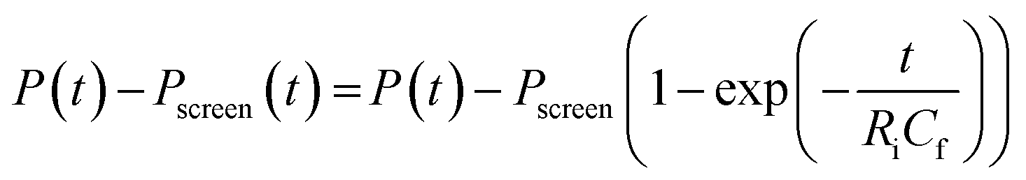 | (14) |
The screening charge builds up at the interface, reducing the effective depolarization field. By introducing this charge screening effect, we’ve adjusted the depolarization field equation to reflect a more accurate depiction of retention behavior.
 | (15) |
By incorporating charge screening, we account for the reduction of the depolarization field over time, which slows down the back-switching process and improves retention.
The adjusted formula shows a moderated depolarization field over time due to the screening charge, leading to a slower rate of polarization decrease (Fig. 7(c)). The detailed parameters utilized for the fitting of our model are delineated in Fig. 7(d), highlighting the derived values of intrinsic switching time (t∞), activation field (α), and time constant (τ). Remarkably, τ exhibited a significant discrepancy between devices, being calculated at 9 µs for those subjected to a low-damage process, as opposed to 700 µs for devices manufactured via conventional methodologies. This difference is attributed primarily to the resistance at the interface layer (Ri), given that the ferroelectric capacitor (Cf) remains consistent across both device types due to the uniform thickness and material used. The marked variance in τ thus suggests a pronounced reduction in the interfacial layer for low-damage processed devices, inferred from considerations of tunneling resistance, which is dependent on the thickness and material of the barrier. This reduction in the interfacial layer is critical, as it directly contributes to the superior short-term retention characteristics observed in ultra-thin ferroelectric films processed with the low-damage technique. Such an approach effectively mitigates the growth of the interfacial layer, which is pivotal in preserving the ferroelectric properties necessary for reliable FeRAM operation. Furthermore, an exhaustive examination of long-term retention characteristics corroborates the enhanced performance of the latter, as detailed in ESI,† Fig. S6.
To ascertain the efficacy of the low-damage metallization process for FeRAM technology, we investigated its impact on the sensing margin, a critical performance parameter. Fig. 8(a) and (b) outline the pulse scheme utilized for stress application and subsequent readout. This scheme involved a stress pulse to polarize the ferroelectric material, followed by a readout pulse to assess the polarization state. The memory window, crucial for state-of-the-art embedded DRAM (eDRAM) technology, is defined by the charge differential between the read bit 1 and read bit 0 pulses, which should ideally exceed 50 fC µm−2 as per industry benchmarks.
 | ||
| Fig. 8 Sensing margin and reliability testing in ferroelectric capacitors. Schematic diagrams showing the pulse scheme used for (a) stress application and (b) readout in ferroelectric capacitors. A stress pulse polarizes the material, and a subsequent readout pulse assesses the polarization state, illustrating how the memory window is determined by the charge differential between the read bit 1 and read bit 0 pulses. (c) Endurance cycling and (d) retention characteristics of ferroelectric capacitors processed via conventional and low-damage methods, demonstrating their ability to endure over 1010 cycles. Retention characteristics were measured at 358 K after 107 cycling. (e) Statistical analysis of the sensing margin for conventional devices, displaying the distribution of sensing margin values across multiple devices (N = 34). The histogram illustrates the variability in sensing margin due to process-induced defects and inconsistencies. (f) Statistical analysis of the sensing margin for low-damage devices, showing a narrower distribution and higher average sensing margin compared to conventional devices. The reduced variance indicates improved uniformity and consistency in device performance resulting from the low-damage metallization process. | ||
Fig. 8(c) and (d) illustrate the endurance cycling and retention characteristics of the ferroelectric capacitors, key indicators of device reliability and performance under repeated use. By applying bipolar pulses with a magnitude of 3.5 MV cm−1 and a duration of 10 µs, we evaluated the memory window across numerous cycles. Both devices demonstrated endurance exceeding 1010 cycles, as shown in Fig. 8(c). Retention tests were conducted at 358 K and involved 107 bipolar cycles to wake up the devices before measurement. The memory window for the device employing the conventional process was observed to exceed 200 fC µm−2. Conversely, the memory window for the same device under a short retention time displayed less than 100 fC µm−2 due to substantial polarization switching triggered by a strong depolarization field, indicative of a low-quality surface state as detailed in Fig. 7. In contrast, the device processed using the low-damage method exhibited superior non-volatility, maintaining its performance over a projected 10-year lifespan, attributable to an enhanced memory window and robust retention characteristics.
To thoroughly assess the performance of the memory window in both conventional and low-damage treated devices, we employed a cumulative distribution function (CDF) analysis. Fig. 8(e) presents the memory window distribution for conventional devices, while Fig. 8(f) shows the corresponding distribution for low-damage treated devices. For this statistical examination, we calculated the mean and standard deviation of the memory window across a large number of measured devices (n = 34). The memory window represents the difference in charge storage between the high and low polarization states. The lower percentiles and upper percentiles (depicted by the black line) were used to highlight the spread of the data across different devices. In both figures, the memory window data are plotted as a function of CDF, with the mean and standard deviation values explicitly displayed. The results show a mean memory window of 82.7 fC µm−2 with a standard deviation of 3.9 fC µm−2 for conventional devices and a significantly improved mean of 342 fC µm−2 with a reduced standard deviation of 3.2 fC µm−2 for low-damage devices. The lower and upper percentile lines closely follow the reference line, indicating that the data are well-distributed without significant outliers. The smaller standard deviation in the low-damage treated devices suggests improved uniformity in the memory window across devices, which can be attributed to the more controlled and less damaging processing environment. This tighter distribution is essential for applications that require consistent performance, as it reduces the risk of variability that could compromise device reliability.
To assess the electrical characteristics of FeRAM at the circuit level, we utilized non-volatile memory simulator (NVSim), a tool renowned for its efficacy in simulating non-volatile memory systems.61 This simulation aimed to compare the performance of MFM capacitors fabricated via conventional and low-damage processes.
Fig. 9(a) illustrates the schematic of the FeRAM read-out operation, highlighting the charge sharing mechanism between the bit line and the MFM capacitor, critical for distinguishing the memory states. As depicted in Fig. 9(b), the memory states, C0 and C1, represent data 0 and data 1, respectively. The C0 state is characterized solely by the Ps value, whereas the C1 state comprises both the 2Pr and the Ps value. The sensitivity of the FeRAM read-out is quantified by the bit line sensing voltage (ΔVBL), calculated as follows:
 | (16) |
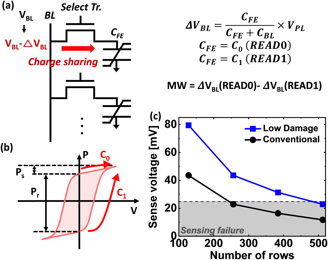 | ||
| Fig. 9 NVSim analysis of FeRAM read-out operation and bit line sensing voltage. (a) Schematic of the FeRAM read-out operation detailing the charge sharing mechanism between the bit line and the MFM capacitor, which is crucial for distinguishing the memory states C0 and C1 in ferroelectric random access memory systems. (b) Illustration of the memory states C0 and C1, where C0 is characterized by the polarization saturation (Ps) value and C1 includes both the double remnant polarization (2Pr) and Ps value. (c) Graph showing the bit line sensing voltage (ΔVBL) across different numbers of rows in memory arrays for capacitors fabricated using both conventional and low-damage processes. The graph highlights the superior performance of the low-damage process in maintaining higher ΔVBL, which is critical for the reliability and functionality of high-density memory arrays. The decreasing trend in ΔVBL as the number of rows increases demonstrates the challenges in scaling and the comparative advantages of the low-damage process. | ||
Conclusion
Throughout this investigation, we have thoroughly analyzed the benefits of the low-damage metallization process in enhancing the properties of ferroelectric capacitors, specifically those using hafnia-based ferroelectric materials. This advanced processing technique significantly impacts the overall performance and reliability of ferroelectric random access memory (FeRAM) devices, which are poised to overcome the limitations faced by traditional DRAM technologies.Firstly, the low-damage process was shown to effectively increase the sensing margin and memory window of FeRAM devices, crucial metrics for their application in high-density memory arrays. Our experimental results demonstrated that capacitors fabricated with this process maintain high polarization values and exhibit reduced wake-up effects, thereby ensuring stable and reliable memory performance over extended periods. This is a marked improvement over capacitors manufactured using conventional processes, where poorer interface quality and higher defect densities lead to performance degradation.
Furthermore, through advanced characterization techniques such as X-ray diffraction, electron energy loss spectroscopy, and high-resolution transmission electron microscopy, we have identified that the superior performance of low-damage process devices is largely due to the minimized formation of detrimental interfacial layers and defect structures. This fine control over the material properties at the nanoscale ensures that the essential characteristics of ferroelectricity are preserved, even under the demanding conditions imposed by modern electronic applications.
The integration of these ferroelectric capacitors with existing CMOS technologies, as explored through simulations with non-volatile memory simulator (NVSim), indicates that the low-damage process not only supports the scalability of ferroelectric memories but also aligns with the industry's push towards higher density memory arrays. Even in high-density configurations, the detectable bit line sensing voltage further validates the utility of the process in enhancing device performance without compromising energy efficiency or operational voltage requirements.
Experimental methods
Device fabrication
p-Type Si substrates doped with boron were thermally oxidized to form a 3000 Å thick SiO2 film. Following this, a 100 nm thick layer of TiN was deposited using DC sputtering as the bottom electrode (BE). A HZO film was then deposited over the TiN layer using plasma-enhanced atomic layer deposition (PEALD) at 300 °C, keeping an Hf:Zr cycle ratio of 1:1. The top electrode (TE), a 10 nm thick TiN layer, was deposited over the HZO films utilizing the same deposition method at 300 °C without breaking the vacuum. Precursors such as tetrakis(ethylmethylamino)hafnium (TEMAHf) and tetrakis(ethylmethylamino)zirconium (TEMAZr) were used for the Hf and Zr sources, respectively, with TiCl4 for the Ti source. Oxygen (O2) gas was used as the oxygen source and ammonia (NH3) as the nitriding source. Following the electrode formation, layers of 10 nm Ti and 30 nm Pt were sequentially evaporated using an electron beam under a shadow mask. The patterned TiN TE was then selectively etched using a NH4OH:H2O2:H2O (1:1:5) solution at 37 °C with Pt serving as the hard mask. For crystallization, the HZO films were subjected to rapid thermal annealing (RTA) at 600 °C for 10 seconds in a nitrogen atmosphere, ensuring the transformation from the amorphous deposited layers to their polycrystalline ferroelectric phase.
Electrical characterization
The ferroelectric characteristics of the films were assessed using a semiconductor parameter analyzer (4200A-SCS, Keithley). High-speed measurements were conducted by the application of trapezoidal pulses (rise and fall time: 10 ns, pulse width: 10 µs) using a 4225-PMU (Keithley Instruments), a pulse generator (81110A, Agilent), and a device current waveform analyzer (CX3324A, Keysight).Material analysis
The crystallographic characteristics and residual stresses of HZO thin films were assessed using grazing incidence X-ray diffraction (GIXRD) conducted on a Rigaku D/MAX-2500 diffractometer. To probe the compositional details, particularly the presence of oxygen vacancies, quantitative analysis of sub-oxide ratios (HfO2−x and ZrO2−x) at the interfaces of the HZO films was carried out using X-ray photoelectron spectroscopy (XPS) with a K-alpha Thermo VG Scientific instrument. In-depth chemical characterization was performed via XPS depth profiling utilizing an Al Kα dual anode radiation source (hν = 1486.6 eV). Systematic etching of the films at three-second intervals using an Ar+ ion beam exposed the subsurface layers. Binding energies were standardized using the C-1s peak at 284.8 eV. The core-level spectra for Hf-4f and Zr-3d were meticulously deconvoluted into Gaussian peaks to determine the relative fractions of sub-oxides within the films. Additionally, the microstructural properties of the films were examined through high-resolution transmission electron microscopy (HR-TEM) and scanning transmission electron microscopy (STEM) using a Titan Cubed G2 60-300 FEI instrument. High-angle annular dark-field scanning transmission electron microscopy (HAADF-STEM) was also employed to provide detailed structural insights into the films.Data availability
The datasets used and/or analyzed during the current study are available from the corresponding author on reasonable request.Conflicts of interest
There are no conflicts to declare.Acknowledgements
This work was supported by the NRF grant funded by the Korea government (MSIT) (no. RS-2023-00260527). This work was also supported by K-CHIPS (Korea Collaborative & High-tech Initiative for Prospective Semiconductor Research) (1415187390, 00231985, 23005-30FC), (2410000582, 00406007, 24051-15TC) and (1415187675, 00235655, 23006-15TC) funded By the Ministry of Trade, Industry & Energy (MOTIE, Korea).References
- S. U. Sharath, S. Vogel, L. Molina-Luna, E. Hildebrandt, C. Wenger, J. Kurian, M. Duerrschnabel, T. Niermann, G. Niu and P. Calka, Control of switching modes and conductance quantization in oxygen engineered HfOx based memristive devices, Adv. Funct. Mater., 2017, 27(32), 1700432 CrossRef.
- P. Buragohain, A. Erickson, T. Mimura, T. Shimizu, H. Funakubo and A. Gruverman, Effect of Film microstructure on domain nucleation and intrinsic switching in ferroelectric Y: HfO2 Thin Film Capacitors, Adv. Funct. Mater., 2022, 32(9), 2108876 CrossRef CAS.
- B. Zeng, C. Liu, S. Dai, P. Zhou, K. Bao, S. Zheng, Q. Peng, J. Xiang, J. Gao and J. Zhao, Electric field gradient-controlled domain switching for size effect-resistant multilevel operations in HfO2-based ferroelectric field-effect transistor, Adv. Funct. Mater., 2021, 31(17), 2011077 CrossRef CAS.
- H. Y. Yoong, H. Wu, J. Zhao, H. Wang, R. Guo, J. Xiao, B. Zhang, P. Yang, S. J. Pennycook and N. Deng, Epitaxial ferroelectric Hf0.5Zr0.5O2 thin films and their implementations in memristors for brain-inspired computing, Adv. Funct. Mater., 2018, 28(50), 1806037 CrossRef.
- F. Xue, Y. Ma, H. Wang, L. Luo, Y. Xu, T. D. Anthopoulos, M. Lanza, B. Yu and X. Zhang, Two-dimensional ferroelectricity and antiferroelectricity for next-generation computing paradigms, Matter, 2022, 5(7), 1999–2014 CrossRef CAS.
- M. H. Park, Y. H. Lee, T. Mikolajick, U. Schroeder and C. S. Hwang, Review and perspective on ferroelectric HfO2-based thin films for memory applications, MRS Commun., 2018, 8(3), 795–808 CrossRef CAS.
- M. Pešić, F. P. G. Fengler, L. Larcher, A. Padovani, T. Schenk, E. D. Grimley, X. Sang, J. M. LeBeau, S. Slesazeck and U. Schroeder, Physical mechanisms behind the field-cycling behavior of HfO2-based ferroelectric capacitors, Adv. Funct. Mater., 2016, 26(25), 4601–4612 CrossRef.
- Z. Li, J. Wu, X. Mei, X. Huang, T. Saraya, T. Hiramoto, T. Takahashi, M. Uenuma, Y. Uraoka and M. Kobayashi, A 3D Vertical-Channel Ferroelectric/Anti-Ferroelectric FET With Indium Oxide, IEEE Electron Device Lett., 2022, 43(8), 1227–1230 CAS.
- M. Hoffmann, A. J. Tan, N. Shanker, Y.-H. Liao, L.-C. Wang, J.-H. Bae, C. Hu and S. Salahuddin, Fast read-after-write and depolarization fields in high endurance n-type ferroelectric FETs, IEEE Electron Device Lett., 2022, 43(5), 717–720 CAS.
- F. Mo, Y. Tagawa, C. Jin, M. Ahn, T. Saraya, T. Hiramoto and M. Kobayashi, Low-voltage operating ferroelectric FET with ultrathin IGZO channel for high-density memory application, IEEE J. Electron Devices Soc., 2020, 8, 717–723 CAS.
- Z. Liang; K. Tang; J. Dong; Q. Li; Y. Zhou; R. Zhu; Y. Wu; D. Han and R. Huang In A novel high-endurance FeFET memory device based on ZrO2 anti-ferroelectric and IGZO channel, 2021 IEEE International Electron Devices Meeting (IEDM), IEEE: 2021; pp 17.3.1-17.3.4.
- J. Hwang, S. Lim, G. Kim, S.-O. Jung and S. Jeon, Non-volatile majority function logic using ferroelectric memory for logic in memory technology, IEEE Electron Device Lett., 2022, 43(7), 1049–1052 CAS.
- D. Das, P. V. Ravindran, C. Park, N. Tasneem, Z. Wang, H. Chen, W. Chern, S. Yu, S. Datta, A. Khan and A. Ge-Channel, Ferroelectric Field Effect Transistor with Logic-Compatible Write Voltage, IEEE Electron Device Lett., 2022, 44(2), 257–260 Search PubMed.
- J. Hwang, H. Joh, C. Kim, J. Ahn and S. Jeon, Monolithically Integrated Complementary Ferroelectric FET XNOR Synapse for the Binary Neural Network, ACS Appl. Mater. Interfaces, 2024, 16(2), 2467–2476 CrossRef CAS.
- N. Feng, H. Li, L. Zhang, N. Ji, F. Zhang, X. Zhu, Z. Shang, P. Cai, M. Li, R. Wang, R. Huang and A. Physics-based, Dynamic Compact Model of Ferroelectric Tunnel Junctions, IEEE Electron Device Lett., 2022, 44(2), 261–264 Search PubMed.
- J. Hwang, Y. Goh and S. Jeon, Effect of insertion of dielectric layer on the performance of Hafnia ferroelectric devices, IEEE Trans. Electron Devices, 2020, 68(2), 841–845 Search PubMed.
- Y. Goh; J. Hwang; M. Kim; M. Jung; S. Lim; S.-O. Jung and S. Jeon In High performance and self-rectifying hafnia-based ferroelectric tunnel junction for neuromorphic computing and TCAM applications, 2021 IEEE International Electron Devices Meeting (IEDM), IEEE: 2021; pp 17.2. 1-17.2. 4.
- J. Hur, C. Park, G. Choe, P. V. Ravindran, A. I. Khan and S. Yu, Characterizing HfO2-Based Ferroelectric Tunnel Junction in Cryogenic Temperature, IEEE Trans. Electron Devices, 2022, 69(10), 5948–5951 CAS.
- S. S. Cheema, N. Shanker, C. H. Hsu, A. Datar, J. Bae, D. Kwon and S. Salahuddin, One nanometer HfO2-based ferroelectric tunnel junctions on silicon, Adv. Electron. Mater., 2022, 8(6), 2100499 CrossRef CAS.
- J. Hwang, Y. Goh and S. Jeon, Physics, Structures, and Applications of Fluorite-Structured Ferroelectric Tunnel Junctions, Small, 2024, 20(9), 2305271 CrossRef CAS.
- J. Wu, F. Mo, T. Saraya, T. Hiramoto, M. Ochi, H. Goto and M. Kobayashi, Monolithic integration of oxide semiconductor FET and ferroelectric capacitor enabled by Sn-doped InGaZnO for 3-D embedded RAM application, IEEE Trans. Electron Devices, 2021, 68(12), 6617–6622 CAS.
- J. Okuno; T. Kunihiro; K. Konishi; H. Maemura; Y. Shuto; F. Sugaya; M. Materano; T. Ali; K. Kuehnel and K. Seidel In SoC compatible 1T1C FeRAM memory array based on ferroelectric Hf0.5Zr0.5O2, 2020 IEEE Symposium on VLSI Technology, IEEE: 2020; pp 1-2.
- K. Tahara; K. Toprasertpong; Y. Hikosaka; K. Nakamura; H. Saito; M. Takenaka and S. Takagi In Strategy toward HZO BEOL-FeRAM with low-voltage operation (≤ 1.2 V), low process temperature, and high endurance by thickness scaling, 2021 Symposium on VLSI Technology, IEEE: 2021; pp 1-2.
- M. Jung, V. Gaddam and S. Jeon, A review on morphotropic phase boundary in fluorite-structure hafnia towards DRAM technology, Nano Convergence, 2022, 9(1), 44 CrossRef CAS PubMed.
- F. Palumbo, C. Wen, S. Lombardo, S. Pazos, F. Aguirre, M. Eizenberg, F. Hui and M. Lanza, A review on dielectric breakdown in thin dielectrics: silicon dioxide, high-k, and layered dielectrics, Adv. Funct. Mater., 2020, 30(18), 1900657 CrossRef CAS.
- M. Pešić, M. Hoffmann, C. Richter, T. Mikolajick and U. Schroeder, Nonvolatile random access memory and energy storage based on antiferroelectric like hysteresis in ZrO2, Adv. Funct. Mater., 2016, 26(41), 7486–7494 CrossRef.
- F. Ali, T. Ali, D. Lehninger, A. Sünbül, A. Viegas, R. Sachdeva, A. Abbas, M. Czernohorsky and K. Seidel, Fluorite-Structured Ferroelectric and Antiferroelectric Materials: A Gateway of Miniaturized Electronic Devices, Adv. Funct. Mater., 2022, 32(27), 2201737 CrossRef CAS.
- Y. Goh, J. Hwang, Y. Lee, M. Kim and S. Jeon, Ultra-thin Hf0.5Zr0.5O2 thin-film-based ferroelectric tunnel junction via stress induced crystallization, Appl. Phys. Lett., 2020, 117(24), 242901 CrossRef CAS.
- D. Zhao, T. Lenz, G. H. Gelinck, P. Groen, D. Damjanovic, D. M. de Leeuw and I. Katsouras, Depolarization of multidomain ferroelectric materials, Nat. Commun., 2019, 10(1), 2547 CrossRef PubMed.
- Y. Lee, Y. Goh, J. Hwang, D. Das and S. Jeon, The influence of top and bottom metal electrodes on ferroelectricity of hafnia, IEEE Trans. Electron Devices, 2021, 68(2), 523–528 CAS.
- P. Yuan, B. Wang, Y. Yang, S. Lv, Y. Wang, Y. Xu, P. Jiang, Y. Chen, Z. Dang and Y. Ding, Enhanced Remnant Polarization (30 µC cm−2) and Retention of Ferroelectric Hf0.5Zr0.5O2 by NH3 Plasma Treatment, IEEE Electron Device Lett., 2022, 43(7), 1045–1048 CAS.
- Y. Goh, J. Hwang, M. Kim, Y. Lee, M. Jung and S. Jeon, Selector-less ferroelectric tunnel junctions by stress engineering and an imprinting effect for high-density cross-point synapse arrays, ACS Appl. Mater. Interfaces, 2021, 13(49), 59422–59430 CrossRef CAS PubMed.
- M. Kim, Y. Goh, J. Hwang and S. Jeon, Enabling large ferroelectricity and excellent reliability for ultra-thin hafnia-based ferroelectrics with a W bottom electrode by inserting a metal-nitride diffusion barrier, Appl. Phys. Lett., 2021, 119(26), 262905 CrossRef CAS.
- Y. Goh, J. Hwang and S. Jeon, Excellent reliability and high-speed antiferroelectric HfZrO2 tunnel junction by a high-pressure annealing process and built-in bias engineering, ACS Appl. Mater. Interfaces, 2020, 12(51), 57539–57546 CrossRef CAS PubMed.
- H. Joh, M. Jung, J. Hwang, Y. Goh, T. Jung and S. Jeon, Flexible ferroelectric hafnia-based synaptic transistor by focused-microwave annealing, ACS Appl. Mater. Interfaces, 2021, 14(1), 1326–1333 CrossRef PubMed.
- J. Hwang, M. Kim, M. Jung, T. Kim, Y. Goh, Y. Lee and S. Jeon, Relatively low-k ferroelectric nonvolatile memory using fast ramping fast cooling annealing process, IEEE Trans. Electron Devices, 2022, 69(6), 3439–3445 CAS.
- J. Hwang, Y. Goh and S. Jeon, Effect of forming gas high-pressure annealing on metal-ferroelectric-semiconductor hafnia ferroelectric tunnel junction, IEEE Electron Device Lett., 2020, 41(8), 1193–1196 Search PubMed.
- X. Lyu; M. Si; X. Sun; M. Capano; H. Wang and P. Ye In Ferroelectric and anti-ferroelectric hafnium zirconium oxide: Scaling limit, switching speed and record high polarization density, 2019 Symposium on VLSI Technology, IEEE: 2019; pp T44-T45.
- S. Oh, H. Kim, A. Kashir and H. Hwang, Effect of dead layers on the ferroelectric property of ultrathin HfZrOx film, Appl. Phys. Lett., 2020, 117(25), 252906 CrossRef CAS.
- Y. Cheng, Z. Gao, K. H. Ye, H. W. Park, Y. Zheng, Y. Zheng, J. Gao, M. H. Park, J.-H. Choi and K.-H. Xue, Reversible transition between the polar and antipolar phases and its implications for wake-up and fatigue in HfO2-based ferroelectric thin film, Nat. Commun., 2022, 13(1), 645 CrossRef CAS.
- T. Schenk, U. Schroeder, M. Pešić, M. Popovici, Y. V. Pershin and T. Mikolajick, Electric field cycling behavior of ferroelectric hafnium oxide, ACS Appl. Mater. Interfaces, 2014, 6(22), 19744–19751 CrossRef CAS.
- M. Hoffmann, U. Schroeder, T. Schenk, T. Shimizu, H. Funakubo, O. Sakata, D. Pohl, M. Drescher, C. Adelmann and R. Materlik, Stabilizing the ferroelectric phase in doped hafnium oxide, J. Appl. Phys., 2015, 118(7), 1–9 CrossRef.
- J. Hwang; C. Kim; H. Shin; H. Kim; S.-H. K. Park and S. Jeon In Ultra-high Tunneling Electroresistance Ratio (2 × 10⁴) & Endurance (10 8) in Oxide Semiconductor-Hafnia Self-rectifying (1.5 × 10³) Ferroelectric Tunnel Junction, 2023 IEEE Symposium on VLSI Technology and Circuits (VLSI Technology and Circuits), IEEE: 2023, pp 1–2.
- H. Shi, H. Huang, J. Bao, J. Liu, P. S. Ho, Y. Zhou, J. T. Pender, M. D. Armacost and D. Kyser, Role of ions, photons, and radicals in inducing plasma damage to ultra low-k dielectrics, J. Vac. Sci. Technol., B: Nanotechnol. Microelectron.: Mater., Process., Meas., Phenom., 2012, 30(1), 1–9 Search PubMed.
- J. Bao, H. Shi, J. Liu, H. Huang, P. Ho, M. Goodner, M. Moinpour and G. Kloster, Mechanistic study of plasma damage of low k dielectric surfaces, J. Vac. Sci. Technol., B: Microelectron. Nanometer Struct.--Process., Meas., Phenom., 2008, 26(1), 219–226 CrossRef CAS.
- T. Czerwiec and D. Graves, Mode transitions in low pressure rare gas cylindrical ICP discharge studied by optical emission spectroscopy, J. Phys. D: Appl. Phys., 2004, 37(20), 2827 CrossRef CAS.
- R. Cui, R. Han, K. Yang, W. Zhu, Y. Wang, Z. Zhang and J. Ouyang, Diagnosis of helicon plasma by local OES, Plasma Sources Sci. Technol., 2020, 29(1), 015018 CrossRef CAS.
- J. Lee, K. Yang, J. Y. Kwon, J. E. Kim, D. I. Han, D. H. Lee, J. H. Yoon and M. H. Park, Role of oxygen vacancies in ferroelectric or resistive switching hafnium oxide, Nano Convergence, 2023, 10(1), 55 CrossRef CAS PubMed.
- H. J. Kim, M. H. Park, Y. J. Kim, Y. H. Lee, T. Moon, K. Do Kim, S. D. Hyun and C. S. Hwang, A study on the wake-up effect of ferroelectric Hf0.5Zr0.5O2 films by pulse-switching measurement, Nanoscale, 2016, 8(3), 1383–1389 RSC.
- S. Zhukov, Y. A. Genenko, O. Hirsch, J. Glaum, T. Granzow and H. von Seggern, Dynamics of polarization reversal in virgin and fatigued ferroelectric ceramics by inhomogeneous field mechanism, Phys. Rev. B: Condens. Matter Mater. Phys., 2010, 82(1), 014109 CrossRef.
- A. Kolmogorov, Statistical theory of nucleation processes, Izu. Akad. Nauk SSSR, 1937, 3, 355–366 Search PubMed.
- N. Gong, X. Sun, H. Jiang, K. Chang-Liao, Q. Xia and T. Ma, Nucleation limited switching (NLS) model for HfO2-based metal-ferroelectric-metal (MFM) capacitors: Switching kinetics and retention characteristics, Appl. Phys. Lett., 2018, 112(26), 262903 CrossRef.
- M. Kobayashi, J. Wu, Y. Sawabe, S. Takuya and T. Hiramoto, Mesoscopic-scale grain formation in HfO2-based ferroelectric thin films and its impact on electrical characteristics, Nano Convergence, 2022, 9(1), 50 CrossRef CAS.
- T. Y. Lee, K. Lee, H. H. Lim, M. S. Song, S. M. Yang, H. K. Yoo, D. I. Suh, Z. Zhu, A. Yoon and M. R. MacDonald, Ferroelectric polarization-switching dynamics and wake-up effect in Si-doped HfO2, ACS Appl. Mater. Interfaces, 2018, 11(3), 3142–3149 CrossRef.
- P. Pujar, H. Cho, Y.-H. Kim, N. Zagni, J. Oh, E. Lee, S. Gandla, P. Nukala, Y.-M. Kim and M. A. Alam, An Aqueous Route to Oxygen-Deficient Wake-Up-Free La-Doped HfO2 Ferroelectrics for Negative Capacitance Field Effect Transistors, ACS Nano, 2023, 17(19), 19076–19086 CrossRef CAS PubMed.
- J.-G. Yoon, B. Kang, J. Kim, T. Noh, T. Song, Y. Lee and J. Lee, Mechanism of Charge Retention Loss in Ferroelectric Pt/Pb (Zr, Ti) O3/Pt Capacitors and Its Relation to Fatigue and Imprint, Integr. Ferroelectr., 2003, 53(1), 401–411 CAS.
- J. Mohan, Y. C. Jung, H. Hernandez-Arriaga, J.-H. Kim, T. Onaya, A. Sahota, S. M. Hwang, D. N. Le, J. Kim and S. J. Kim, Relaxation Induced by Imprint Phenomena in Low-Temperature (400 °C) Processed Hf0.5Zr0.5O2-Based Metal-Ferroelectric-Metal Capacitors, ACS Appl. Electron. Mater., 2022, 4(4), 1405–1414 CrossRef CAS.
- C. T. Black and J. J. Welser, Electric-field penetration into metals: consequences for high-dielectric-constant capacitors, IEEE Trans. Electron Devices, 1999, 46(4), 776–780 CrossRef CAS.
- A. Kashir, H. Kim, S. Oh and H. Hwang, Large remnant polarization in a wake-up free Hf0.5Zr0.5O2 ferroelectric film through bulk and interface engineering, ACS Appl. Electron. Mater., 2021, 3(2), 629–638 CrossRef CAS.
- X. Lou, Polarization retention on short, intermediate, and long time scales in ferroelectric thin films, J. Appl. Phys., 2009, 105(9), 094107 CrossRef.
- X. Dong, C. Xu, Y. Xie and N. P. Jouppi, Nvsim: A circuit-level performance, energy, and area model for emerging nonvolatile memory, IEEE Trans. Comput.-Aided Des. Integr. Circuits System., 2012, 31(7), 994–1007 Search PubMed.
Footnote |
| † Electronic supplementary information (ESI) available. See DOI: https://doi.org/10.1039/d4tc02460e |
| This journal is © The Royal Society of Chemistry 2025 |