
 Open Access Article
 This Open Access Article is licensed under a Creative Commons Attribution-Non Commercial 3.0 Unported Licence
Unmasking the magic of magic blue in perovskite doping†
Zuzanna
Molenda
 ab,
Guillaume
Wantz
a,
Sylvain
Chambon
a,
Dario M.
Bassani
b and
Lionel
Hirsch
*a
ab,
Guillaume
Wantz
a,
Sylvain
Chambon
a,
Dario M.
Bassani
b and
Lionel
Hirsch
*a
aUniv. Bordeaux, CNRS, Bordeaux INP, IMS, UMR 5218, F-, 33400, Talence, France. E-mail: lionel.hirsch@ims-bordeaux.fr
bUniv. Bordeaux, CNRS, Bordeaux INP, ISM UMR 5255, F-, 33400, Talence, France
First published on 12th September 2024
Abstract
The broader utilization of perovskite semiconductors in electronic devices is constrained by the inherent challenge of doping these materials. Magic blue (tris(4-bromophenyl) ammoniumyl hexachloroantimonate) is a cationic salt which, once introduced in a polycrystalline film of a methylammonium lead iodide (CH3NH3PbI3 or MAPI) perovskite, increases the conductivity up to 30 times and shifts the Fermi level by about 100 meV towards the valence band. The latter is confirmed via surface potential measurements using Kelvin probe and ultraviolet photoelectron spectroscopy. The photoluminescence quenching of the doped samples confirms the presence of an excess of free charge carriers, while the optical bandgap remains unchanged. The doping mechanism most likely resembles molecular charge transfer doping, with the electron transfer from MAPI to the ammoniumyl cation occurring at grain boundaries of the polycrystalline perovskite film.
1. Introduction
Metal halide perovskites (MHPs) are promising candidates for preparing semiconductors for next generation electronic devices, with solar cells as their prime example.1–6 Perovskite-based solar cells and LEDs have attained efficiencies close to their thermodynamic limits7,8 using charge selective contacts that allow mimicking the p–i–n or n–i–p device structure by employing contacts of different work functions and charge selective interlayers. The devices that employ classic semiconductors (Si, GaAs, etc.) introduce p- and n-type dopants to achieve charge selectivity and generate a built-in potential. Perovskite doping would thereby allow simplifying device fabrication processes and open new application possibilities, such as field effect transistors, in which well-defined n- and p-type zones are essential. Other advantages of this class of semiconductors include facile synthesis, inexpensive precursors, high defect tolerance9 and bandgap tunability.Perovskite doping, however, must overcome more obstacles than those faced by classical semiconductors, notably due to the ionic character of the perovskite crystal and the electroneutrality of the precursor solutions. This implies that any heterovalent dopant is accompanied by a requisite number of counter ions that cancels out the potential doping effect. In addition, heterovalent dopants are unlikely to be incorporated in the crystal structure of the perovskite. So far, to the best of our knowledge, only one report of substitutional doping using a heterovalent element has been reported,10 using Sm2+ to replace Pb2+ during the crystallization step, followed by its spontaneous oxidation to Sm3+. This results in the release of an electron to the conduction band of the material, leading to n-type doping. This approach requires a careful selection of the dopant, which must be metastable at the oxidation state +2 to substitute Pb2+ and stable at +3 for n-type doping and +1 for p-type doping. The radius of the doping ion should also be the closest possible to the one of the substituted metal.
Among the recent reports on perovskite doping, the most common approach is inspired by the field of organic semiconductors and is based on electron transfer from the perovskite to the dopant for p-type and from the dopant to the perovskite for n-type11–16 doping. Molecular charge transfer doping involves adding a compound whose LUMO energy level is below that of the HOMO or valence energy (EV) of the host for p-type. This induces electron transfer from the EV to the LUMO level, depleting the EV of electrons which therefore increases the hole density and shifts the Fermi level (EF) towards EV. The opposite is true for n-type doping. The dopant is typically an organic molecule much larger than the perovskite unit cell. Thus, the dopant is not incorporated within the perovskite crystalline domains and is instead located at grain boundaries or at the surface of the film. This type of doping has met with some success,12,14 notably for the p-type doping of CH3NH3Pb0.5Sn0.5I3, using tetrafluorotricyanoquinine (F4TCNQ).11 This dopant possesses a LUMO level at −5.24 eV that is well-suited for mixed-metal perovskites possessing high EV. Efficient charge transfer is manifested with a conductivity increase of around 5 orders of magnitude upon doping. However, the same approach is inefficient for CH3NH3PbI3 as its EV is higher, rendering electron transfer less likely. Considering that to date only lead-based perovskites exhibit reasonable device stability and efficiency, most doping studies should focus on these materials.
A recently published work shows both p- and n-type molecular dopants of the FA0.75Cs0.25Pb(I0.92Br0.08)3, introduced by the co-evaporation method.15 However, as reported by the authors, it is difficult to achieve doping for methylammonium-containing perovskites, as the MAI precursor has been proven to be difficult to evaporate reliably due to its high vapor pressure and thermal instabilities.17–19 Therefore, identifying a transvelsal p-type dopant, suitable for many perovskite formulations and solution-processable, is still of significant importance.
Tris(4-bromophenyl) ammoniumyl hexachloroantimonate, also called magic blue (MB), has recently experienced a renaissance as a dopant for organic semiconductors.20–24 For instance, Feaugas et al.25 used it as a dopant for the PTQ10:ITIC-4F blend, leading to an increase in conductivity and work function (WF) for dopant concentrations >10% (molar ratio). The doped layer serves as an efficient hole transporting layer, avoiding the use of hygroscopic PEDOT:PSS. Lee et al.26 showed that MB can be incorporated between the organic spacers in the butylammonium–methylammonium lead iodide (BA2MAn−1PbnI3n+1) 2D Ruddelsen–Poppers perovskite. The study, although primarily centred on the 2D structure, opens a gateway to broader explorations within the domain of 3D perovskites. Herein, we report our investigation of the use of MB to dope MAPI, a 3D perovskite. Our findings not only shed light on the unique doping mechanisms in the 3D context, but also hint at potential applications and considerations for the 3D counterparts.
2. Methods
2.1. Materials
Methylammonium iodide (CH3CN3I, >4 N) was purchased from GreatCell Solar Materials. All the following precursors and solvents were purchased from Merck and stored in a glove box under an inert atmosphere: lead(II) iodide (PbI2, 99.999%, perovskite grade), tris(4-bromophenyl)ammoniumyl hexachloroantimonate ([(4-BrC6H4)3N]SbCl6, technical grade) and N,N-dimethylformamide, anhydrous (98.8%).2.2. Substrates
Glass substrates with patterned gold electrodes were used for the conductivity measurements. Glass substrates covered with a thin layer of ITO (10 Ω sq−1) were used for the surface potential difference measurements (Kelvin probe) and ultraviolet photoelectron spectroscopy (UPS).2.3. Sample fabrication
The substrates were cleaned in a sonication bath first with Hellmanex™ III solution (Sigma Aldrich) and in DI water for 15 minutes each, and then in isopropanol (4 N) for 10 min. Subsequently, they were treated with UV-ozone for 15 minutes. Sample fabrication was performed under a controlled nitrogen atmosphere in a glove box. The perovskite precursor solutions consisted of 1.5 M PbI2 and 1.5 M MAI dissolved in DMF by stirring at 60 °C for around 20 min. The MB was dissolved in DMF with concentrations of 50 or 200 mg mL−1 by energetic shaking at RT right before adding the appropriate amount to the perovskite solutions in order to obtain 0.5 mL solutions with the MB/perovskite molar ratios of 0, 0.1%, 0.2%, 0.5%, 1% and 5%. The solutions were filtered through a 0.45 μm PTFE filter and spin coated on appropriate substrates at a spin rate of 3000 rpm for 30 s. After 5 s, 0.3 mL of diethyl ether was dropped onto the spinning substrate. The samples were then annealed on a hot plate for 10 min at 100 °C. The perovskite film thickness was around 600 nm. A 200 mg mL−1 MB solution was used to fabricate bare MB films by spin coating at 1000 rpm for 30 s. The films were then dried on a hot plate at 100 °C for 10 min. The resulting films were around 20 nm thick.2.4. Characterization
Conductance was measured between two symmetric Ti/Au electrodes (10 and 50 nm, respectively) with the distance 200 μm between them, deposited on the glass substrates using the electron beam evaporator. The perovskite layer was then spin coated on top of the electrodes. Conductivity was calculated from the IV curves of the 250 nm thick film spin-coated on the glass substrate with gold electrodes thermally evaporated on the top. The data were collected using a Keithley 4200 source meter unit (SMU). The samples were scanned from −1 V to 1 V at a rate of 5 mV s−1. The WF was measured using a Kelvin probe station from Besocke Delta Phi. Absorbance and photoluminescence spectra were recorded using a Shimadzu UV-3600 Plus UV-Vis-NIR spectrophotometer or a Photon Technology International setup, model: P21LRXS-LNN-NS-17, respectively. A Bruker Innova NanoScope instrument was used in tapping mode to obtain AFM images of the sample's surface. UPS was performed with a PHOIBOS 100 hemispherical energy analyzer equipped with a SPECS UVS 10/35 light source. Conductance measurements were performed in a glovebox. Ultraviolet photoelectron spectra were obtained under vacuum with the samples transferred using a nitrogen-filled transfer box which was only opened in the measurement chamber when sufficient vacuum was obtained. AFM and surface potential difference measurements were performed in air. Absorption and PL spectra were obtained on encapsulated samples.3. Results and discussion
The MB p-type doping was performed on 3D MAPI perovskite thin films as these have been widely studied. As a first assessment of the changes of the charge carrier density, we compared the conductivity of the undoped polycrystalline MAPI film with those of MB-doped films with a concentration of 0.1–5%. A conductivity increase is observed even for the lowest concentration used (Fig. 1) with an average of nearly 16-fold increase (from 11.4 ± 1.8 nS cm−1 to 180.3 ± 42.7 nS cm−1) and a maximum of 30-fold increase for 1% MB (from 8 nS cm−1 for the undoped to 240 nS cm−1 for 1% MB). At doping concentrations greater than 1%, the conductivity stabilizes, indicating a probable limit for this system. | ||
| Fig. 1 Conductivity as a function of doping concentration. | ||
To confirm the change in the majority carrier type, the WF of the undoped and doped MAPI, as well as that of the MB layer alone, was determined from the secondary cut-off of the UPS. The WF of the undoped MAPI film is 4.45 eV and increases to 4.57 eV for the 1% doping. This trend is confirmed by the surface potential measurements using a Kelvin probe, even though the values are higher by 0.5 eV for the perovskite samples and 0.2 eV for the MB film. This discrepancy stems probably from different ambient (air for the Kelvin probe vs. vacuum for the UPS), therefore traces of oxygen or water could adsorb to the sample surface, increasing its WF. Additionally, Kelvin probe is known to be sensitive to surface impurities and MB undergoes slow oxidative dimerization in the solid to form products that are also strong oxidants.27 Nevertheless, both UPS and Kelvin probe confirm the increase of the WF of the doped perovskite upon doping. The WF of the MB at the level of 5.7 eV is in agreement with a previous study by Feaugas et al.25
In order to confirm that the MB doping does not affect the bandgap of the perovskite, the absorbance spectra of the doped and undoped samples were compared. All the spectra are typical for MAPI, with comparable absorbance in the measured region. The bandgap (Eg) determined from the Tauc plots is between 1.62 and 1.63 eV. A small bandgap widening (∼10 meV) might be a result of the filling the shallow traps, just above the EV, by the excess of holes, upon doping. For 5% of MB, the Eg increases to 1.66 eV. This result shows that the conductivity increase cannot be due to the presence of additional electronic states within the bandgap, nor due to the bandgap narrowing due to defects or lattice distortion.
Doping may be evidenced from the increase of the free charge carrier density, which may be indirectly deduced from photoluminescence (PL) measurements. The PL spectra of the undoped and doped MAPI are shown in Fig. 4. The maximum PL intensity falls at 765 nm for all the samples and this is in agreement with the bandgap value of MAPI. The average PL signal is almost 3 times less intense upon doping with 0.1% MB and 7 and 6.5 times less intense for the doping concentrations of 0.5% and 1%, respectively. Our results are consistent with what is usually observed in doped semiconductors. Due to the presence of free charge carriers (here free holes), the lifetime shortening of minority carriers leads to a strong quenching of the luminescence.28–30 For 5% MB, two weak peaks can be observed, one at 756 nm, belonging to MAPI, and another at 793 nm, that belongs to MB (ESI†). This information, together with the “saturation” of conductivity for 5% MB and the shift of the absorption edge, points to a possible phase separation for the highest doping concentrations.
Ultraviolet photoelectron spectroscopy (UPS) allows investigation of the electronic properties of a semiconductor at its bandgap edges. Fig. 5a shows the onset of the valence energies for the doped and undoped samples. It can be seen that the energy with respect to the Fermi level (E w.r.t. EF) decreases by 0.1 eV upon doping with MB at 0.1% and 1%. This result is consistent with the increase of the WF found from the UPS cutoff and surface potential difference measurements (Fig. 2). Both HOMO and LUMO levels, together with the unaltered Eg, are presented in Fig. 5b, where the shift of the EF of the perovskite thin film upon doping with MB can be clearly observed.
 | ||
| Fig. 2 UV-vis absorption spectra and Tauc plots is shown in the inset. | ||
UPS analysis was also carried-out for a thin film of pure MB. The latter evidences MB's strong electron-accepting character consistent with a high EA. The energy level of the singly occupied molecular orbital (SOMO) determined from UPS (ca. 5.45 eV, see Fig. 3) is not far from the value of the EA estimated by Zhang et al. using cyclic voltammetry (5.5 eV).31 This suggests that ionization of MB occurs from the SOMO or that its energy level is close to that of the highest fully-occupied molecular orbital from which ionization occurs (Fig. S3, ESI†).32 The doping process of MAPI is therefore proposed to occur through electron transfer from the perovskite valence band (Ev = −5.3 eV) to the partially-filled SOMO of the MB, leading to p-type doping of the perovskite. The driving force for electron transfer may be estimated to be ca. −0.3 eV from the difference in ionization potential of MAPI and the EA of MB. In this context, the doping mechanism exhibits similarities to molecular charge transfer doping previously reported by Euvrard et al.11 AFM images of the doped vs. undoped MAPI show that doping results in a modest decrease of the grain size (Fig. S2, ESI†). Taking into account the size of the MB molecule, as well as the ionic character of the perovskite crystal, it is very likely that the dopant is located at the grain boundaries. This would limit electron transfer doping by MB to the interfacial intergrain region. The roll-off of the conductivity observed upon increasing the dopant level may therefore reflect the localized nature of the doping as well as the formation of reduced MB (an electrical insulator) in the intergrain region.
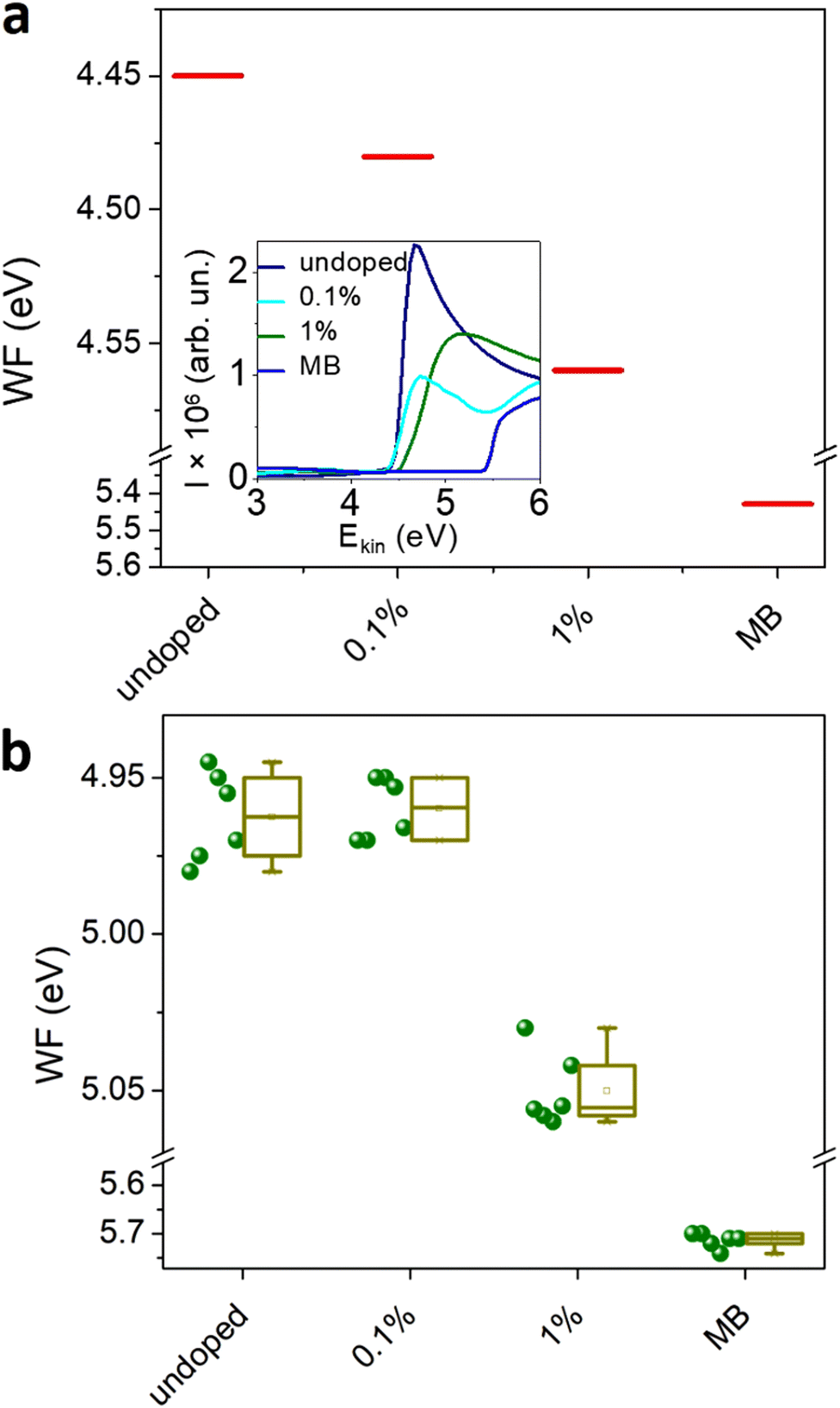 | ||
| Fig. 3 WF determined from (a) UPS secondary cut-off and (b) surface potential difference measurement, using a Kelvin probe. | ||
 | ||
| Fig. 4 (a) Photoluminescence as a function of the doping concentration. (b) PL intensity as a function of the doping concentration. | ||
 | ||
| Fig. 5 (a) Valence band region of the UPS spectra for undoped and doped MAPI. (b) EF shift upon doping with MB as well as the SOMO and EF of a MB thin film. The SOMO level of MB is estimated from UPS assuming that it is the highest (partly) occupied molecular orbital. Ec and Ev represent the energy of the conduction and valence band of MAPI, respectively. Filled states are black, empty blue, and EF red. | ||
4. Conclusions
We demonstrate a simple, spin-coating route for MAPI p-type doping, where tris(4-bromophenyl) ammoniumyl hexachloroantimonate, commonly known as magic blue, is blended into a polycrystalline perovskite film. The doping mechanism resembles the molecular charge transfer doping, where electron transfer takes place from the perovskite valence band to the HOMO level of the MB, rendering the perovskite p-type. The quenching of the MAPI's photoluminescence suggests the presence of free charges. The UPS measurement confirmed the shift of the MAPI's EF towards the EV by around 0.1 eV.We believe that these results can shed light on how a careful selection of the dopant can influence and optimize the performance and properties of perovskite semiconductors, thereby advancing the development of more efficient and stable electronic devices. This still understudied field is soon expected to be fluorishing, considering the possibility of the development of MHPs towards energy-effective electronics.
Author contributions
GW proposed the dopant. ZM planned and performed the experiments, analysed the data and wrote the first draft of this article. All the authors participated in constructive discussions and the final version of this article.Data availability
The data supporting this article have been included as part of the ESI.†Conflicts of interest
There are no conflicts of interest to declare.Acknowledgements
The Agence Nationale de la Recherche (HYPERSOL project no. ANR-18-CE05-0021-01) and the Region Nouvelle Aquitaine (STRIPE project no. 2019-1R1M08) are gratefully acknowledged for their financial support. UPS analyses were performed at the ELORPrintTec facility with the help of Roland Lefèvre.References
- E. H. Anaraki, A. Kermanpur, L. Steier, K. Domanski, T. Matsui, W. Tress, M. Saliba, A. Abate, M. Grätzel, A. Hagfeldt and J.-P. Correa-Baena, Energy Environ. Sci., 2016, 9, 3128–3134 RSC.
- D. B. Khadka, Y. Shirai, M. Yanagida, J. W. Ryan and K. Miyano, J. Mater. Chem. C, 2017, 5, 8819–8827 RSC.
- D. Barrit, P. Cheng, M. C. Tang, K. Wang, H. Dang, D. M. Smilgies, S. Liu, T. D. Anthopoulos, K. Zhao and A. Amassian, Adv. Funct. Mater., 2019, 29, 1807544 CrossRef CAS.
- X. Bao, Y. Wang, Q. Zhu, N. Wang, D. Zhu, J. Wang, A. Yang and R. Yang, J. Power Sources, 2015, 297, 53–58 CrossRef CAS.
- J. V. Patil, S. S. Mali and C. K. Hong, ACS Sustainable Chem. Eng., 2020, 8, 16364–16371 CrossRef CAS.
- Z. Molenda, S. Chambon, D. M. Bassani and L. Hirsch, Eur. J. Inorg. Chem., 2021, 2533–2538 CrossRef CAS.
- J. Park, J. Kim, H. S. Yun, M. J. Paik, E. Noh, H. J. Mun, M. G. Kim, T. J. Shin and S. I. Seok, Nature, 2023, 616, 724–730 CrossRef CAS PubMed.
- M. A. Green, E. D. Dunlop, J. Hohl-Ebinger, M. Yoshita, N. Kopidakis, K. Bothe, D. Hinken, M. Rauer and X. Hao, Prog. Photovoltaics Res. Appl., 2022, 30, 687–701 CrossRef.
- D. H. Fabini, R. Seshadri and M. G. Kanatzidis, MRS Bull., 2020, 45, 467–477 CrossRef.
- Z. Molenda, B. Politi, R. Clerc, M. Abbas, S. Chambon, D. M. Bassani and L. Hirsch, Mater. Horiz., 2023, 10, 2845–2853 RSC.
- J. Euvrard, O. Gunawan, X. Zhong, S. P. Harvey, A. Kahn and D. B. Mitzi, Mater. Adv., 2021, 2, 2956–2965 RSC.
- N. K. Noel, S. N. Habisreutinger, A. Pellaroque, F. Pulvirenti, B. Wenger, F. Zhang, Y. H. Lin, O. G. Reid, J. Leisen, Y. Zhang, S. Barlow, S. R. Marder, A. Kahn, H. J. Snaith, C. B. Arnold and B. P. Rand, Energy Environ. Sci., 2019, 12, 3063–3073 RSC.
- D. Parobek, B. J. Roman, Y. Dong, H. Jin, E. Lee, M. Sheldon and D. H. Son, Nano Lett., 2016, 16, 7376–7380 CrossRef CAS PubMed.
- E. A. Gaulding, J. Hao, H. S. Kang, E. M. Miller, S. N. Habisreutinger, Q. Zhao, A. Hazarika, P. C. Sercel, J. M. Luther and J. L. Blackburn, Adv. Mater., 2019, 31, 1–9 CrossRef PubMed.
- T. Schramm, M. Deconinck, R. Ji, E. Siliavka, Y. J. Hofstetter, M. Löffler, V. V. Shilovskikh, J. Brunner, Y. Li and S. Bitton, et al. , Adv. Mater., 2024, 2314289 CrossRef CAS PubMed.
- Q. Ou, Y. Zhang, Z. Wang, J. A. Yuwono, R. Wang, Z. Dai, W. Li, C. Zheng, Z. Q. Xu, X. Qi, S. Duhm, N. V. Medhekar, H. Zhang and Q. Bao, Adv. Mater., 2018, 30, 1–10 Search PubMed.
- J. Ávila, C. Momblona, P. P. Boix, M. Sessolo and H. J. Bolink, Joule, 2017, 1, 431–442 CrossRef.
- S. Wang, L. K. Ono, M. R. Leyden, Y. Kato, S. R. Raga, M. V. Lee and Y. Qi, J. Mater. Chem. A, 2015, 3, 14631–14641 RSC.
- E. J. Juarez-Perez, Z. Hawash, S. R. Raga, L. K. Ono and Y. Qi, Energy Environ. Sci., 2016, 9, 3406–3410 RSC.
- S. Oh, P. H. Nguyen, T. M. Tran, A. J. DeStefano, K. Tagami, D. Yuan, A. Nikolaev, M. Condarcure, S. Han and J. R. de Alaniz, et al. , J. Mater. Chem. C, 2023, 11, 15435–15442 RSC.
- K. Singh, A. A. Mohapatra, D. Giri, C. Gangadharappa, S. Jhulki, S. Barlow, S. R. Marder, A. Ghosh, S. Patil and N. Chauhan, ACS Appl. Electron. Mater., 2023, 5, 6765–6777 CrossRef CAS.
- D. W. Burke, R. R. Dasari, V. K. Sangwan, A. K. Oanta, Z. Hirani, C. E. Pelkowski, Y. Tang, R. Li, D. C. Ralph and M. C. Hersam, et al. , J. Am. Chem. Soc., 2023, 145, 11969–11977 CrossRef CAS PubMed.
- S.-W. Kim, H. Jung, M. S. Okyay, H.-J. Noh, S. Chung, Y. H. Kim, J.-P. Jeon, B. M. Wong, K. Cho and J.-M. Seo, et al. , Angew. Chem., Int. Ed., 2023, 62, e202310560 CrossRef CAS PubMed.
- A. I. Hofmann, R. Kroon, S. Zokaei, E. Järsvall, C. Malacrida, S. Ludwigs, T. Biskup and C. Müller, Adv. Electron. Mater., 2020, 6, 1–8 Search PubMed.
- F. Feaugas, T. Nicolini, G. H. Roche, L. Hirsch, O. J. Dautel and G. Wantz, Sol. RRL, 2023, 7, 1–8 Search PubMed.
- J. Lee, K.-Y. Baek, J. Lee, H. Ahn, Y. Kim, H. Lim, Y. Kim, J. Woo, S. D. Stranks and S. K. Lee, et al. , Adv. Funct. Mater., 2023, 2302048 CrossRef CAS.
- M. R. Talipov, M. M. Hossain, A. Boddeda, K. Thakur and R. Rathore, Org. Biomol. Chem., 2016, 14, 2961–2968 RSC.
- M. Liu, A. H. Kitai and P. Mascher, J. Lumin., 1992, 54, 35–42 CrossRef CAS.
- D. Kouyate, J. C. Ronfard-Haret, P. Valat, J. Kossanyi, U. Mammel and D. Oelkrug, J. Lumin., 1990, 46, 329–337 CrossRef CAS.
- M. Leroux, N. Grandjean, B. Beaumont, G. Nataf, F. Semond, J. Massies and P. Gibart, Phys. Status Solidi B, 1999, 216, 605–608 CrossRef CAS.
- S. Zhang, H. M. Hill, K. Moudgil, C. A. Ritcher, A. R. Hight Walker, S. Barlow, S. R. Marder, C. A. Hacker and S. J. Pookpanratana, Adv. Mater., 2018, 30, 1802991 CrossRef PubMed.
- S. Kasemthaveechok, L. Abella, J. Crassous, J. Autschbach and L. Favereau, Chem. Sci., 2022, 13, 9833–9847 RSC.
Footnote |
| † Electronic supplementary information (ESI) available. See DOI: https://doi.org/10.1039/d4tc02149e |
| This journal is © The Royal Society of Chemistry 2024 |