
Observation of the planar Hall effect in the quasi-two-dimensional topological insulator candidate Ni3Bi2Se2†
Yuzhe
Ma
ab,
Wen
Sun
ab,
Qiunan
Xu
c,
Xinming
Wang
bd,
Aisha
Aqeel
efg and
Guowei
Li
 *ab
*ab
aCAS Key Laboratory of Magnetic Materials and Devices, Ningbo Institute of Materials Technology and Engineering, Chinese Academy of Sciences, Ningbo 315201, China. E-mail: liguowei@nimte.ac.cn
bUniversity of Chinese Academy of Sciences, 19 A Yuquan Rd, Shijingshan District, Beijing 100049, China
cQingdao Institute for Theoretical and Computational Sciences Shandong University, Qingdao 266237, China
dPublic Technical Service Center, Ningbo Institute of Materials Technology and Engineering, Chinese Academy of Sciences, Ningbo 315201, China
ePhysics Department, Technical University of Munich, Garching, Germany
fMunich Center for Quantum Science and Technology (MCQST), Munich, Germany
gInstitute of Physics, University of Augsburg, Augsburg, Germany
First published on 19th July 2024
Abstract
The observation of the planar Hall effect (PHE) sheds light on the spin textures and topological characteristics of materials, indicating potential applications in quantum computing and electronic devices. However, in bulk single crystals of topological insulators (TIs), where chiral anomaly is absent and the contribution of topological surface states can be overlooked, the origin of the PHE remains elusive. Here, we have obtained high-quality single crystals of Ni3Bi2Se2 and systematically investigated their magneto-electric transport properties. The ordinary Hall resistivity reveals the simultaneous presence of electrons and holes. A π-period PHE, which depends on the relative angle with the driving electric and magnetic fields, has been observed, indicating the breaking of mirror reflection symmetry. The angular dependence of in-plane anisotropic magnetoresistance and the field-dependent PHE signal underscore the critical role of anisotropic orbital magnetoresistance. Our findings offer a platform for deepening our understanding of the PHE and its underlying mechanisms in TIs.
 Guowei Li | Guowei Li is currently a principal investigator at the Ningbo Institute of Materials Technology & Engineering, Chinese Academy of Sciences, and the head of the Magnetic Materials for Energy Conversion group. He received his PhD degree from the University of Groningen in 2016 and subsequently served as a post-doctoral fellow and a group leader at the Max Planck Institute for Chemical Physics of Solids. His expertise and interests primarily focus on the growth of topological/magnetic single crystals, spin chemistry, and topological catalysis. In 2024, he was awarded a leadership position in the Max Planck Partner Group. |
Introduction
In-plane anisotropic magnetoresistance (PAMR) and the planar Hall effect (PHE) refer to the variations in the in-plane longitudinal and transverse resistivity of a material, respectively, as a function of the angle between the in-plane current and the magnetic field. These phenomena have widespread application in tunneling magnetoresistive devices, magnetic sensors, and spintronic devices.1–4 The remarkable advancements in the field of topological quantum matter over the last two decades have sparked significant interest in investigating these effects. In topological semimetals exhibiting a chiral anomaly, chiral charges are transferred between two Weyl nodes of opposite chirality when the electric and magnetic fields are coplanar. The PHE manifests with an increasing magnetic field and has also been considered as additional evidence for identifying the Weyl/Dirac nature of materials, alongside negative magnetoresistance (NMR).5–11 To date, such phenomena have been documented in various topological semimetals, including ZrTe5,12 GdPtBi,7 WTe2,10 VAl3,13 and so on.14,15 Additionally, several other physical mechanisms have been proposed to explain the PHE, such as spin–orbit coupling, in-plane orbital magnetoresistance anisotropy, and anisotropic magnetic backscattering.In contrast, topological insulators (TIs) do not inherently exhibit a chiral anomaly, presenting a significant opportunity to unravel the origin of the PHE. However, the observation of the PHE and its origin within these materials remain obscure. Taskin et al. suggested that the PHE in TIs could be due to the anisotropic scattering rate, which stems from the anisotropic polarization of magnetic impurities.16 However, Zheng et al. proposed that the PHE mainly comes from anisotropic backscattering, which arises from the tilt of the Dirac cone with nonlinear momentum terms induced by an in-plane magnetic field.17 Beyond this, a quasi-classical theory related to Boltzmann transport equations was proposed, which indicates that the PHE signal can be induced by the Berry curvature of the conduction band in three-dimensional (3D) TIs even without chiral anomaly.18 Recent research on Bi1.1Sb0.9Te2S has shown that the spin-momentum locking surface states of the TI are crucial for the PHE, which can be attributed to the differential backscattering forbiddance for Dirac fermions of varying spins under a planar magnetic field.19 Given the theoretical propositions and their associated controversies, there is a pressing need to investigate new potential TI materials that exhibit the PHE.
Compounds with the chemical formula M3A2B2 (where M = Ni, Co, Rh, Pd, and Pt; A = In, Tl, Sn, Pb, and Bi; B = S and Se) have garnered substantial interest for their complex topological nature and unique physical properties. Examples include the ferromagnetic Weyl semimetal Co3Sn2S2, notable for its exceptionally large anomalous Hall conductivity, PHE, and NMR.20–23 The kagome metals Ni3In2S2 and Pd3Bi2S2 are recognized for their infinite Dirac nodal lines, extraordinarily high mobility, and magnetoresistance (MR).24–26 Given these precedents, the parkerite compound Ni3Bi2Se2 has captured our interest because of the observation of superconductivity.27 More recently, it has been predicted to exhibit a 3D topological insulator phase.28,29 Moreover, first-principles calculations predict that Ni3Bi2Se2 exhibits a three-dimensional strong TI phase with Z2 invariants (1;111) (Table S1, ESI†). This is distinct from the two-dimensional topological insulator with a corresponding Chern invariant.30,31 This makes it a promising platform for investigating the PHE and other exotic physical phenomena, such as topological superconductivity.
In this study, we have successfully synthesized Ni3Bi2Se2 single crystals using the Bi flux method and have comprehensively characterized their transport properties. The MR demonstrates notable anisotropy, reaching 12% for the magnetic field perpendicular (B⊥) to the ab plane and approximately 1% for the magnetic field parallel (B‖) to the ab plane, under a 9 T magnetic field at 2 K with the current flowing within the ab plane. Additionally, a distinct PHE signal with π periodicity was observed when the external magnetic field was applied in a coplanar orientation with the current in the ab plane. Further analysis indicates that the PHE is primarily due to the anisotropy of the in-plane orbital magnetoresistance.
Experimental details
Ni3Bi2Se2 single crystals were synthesized using a flux growth method, utilizing excess Bi as the flux. The starting materials consisted of Ni powder (99.99% purity), Bi shot (99.99% purity), and Se powder (99.99% purity), which were measured in a molar ratio of 1![[thin space (1/6-em)]](https://www.rsc.org/images/entities/char_2009.gif) :3:1.2. These materials were placed into a fritted alumina crucible set (referred to as a Canfield Crucible Set)32 and then sealed in a fused quartz tube under a partial argon pressure. The tube was subsequently heated to 1000 °C over 6 hours, maintained at this temperature for 20 hours, then cooled to 900 °C over 4 hours and held at this temperature for 10 hours. Following this, it was slowly cooled to 550 °C at a rate of 3 °C/hour. At this temperature, the remaining liquid was separated from the crystals through a centrifugation process.33
:3:1.2. These materials were placed into a fritted alumina crucible set (referred to as a Canfield Crucible Set)32 and then sealed in a fused quartz tube under a partial argon pressure. The tube was subsequently heated to 1000 °C over 6 hours, maintained at this temperature for 20 hours, then cooled to 900 °C over 4 hours and held at this temperature for 10 hours. Following this, it was slowly cooled to 550 °C at a rate of 3 °C/hour. At this temperature, the remaining liquid was separated from the crystals through a centrifugation process.33
The crystal structure of the as-grown single crystals was determined using a Bruker D8 ADVANCE diffractometer (Cu Kα radiation, λ = 1.54178 Å) operating at a voltage of 40 kV and a current of 40 mA at 293 K. The single crystal X-ray diffraction (SXRD) data of Ni3Bi2Se2 were collected using a Bruker D8 VENTURE single crystal diffractometer with multilayer monochromatized Mo Kα radiation (λ = 0.71073 Å) at 223 K, and the crystal structure was solved by direct methods and refined by the full-matrix least-squares method on F2 with the SHELXL software.34,35 The composition characterization was carried out using a scanning electron microscope (SEM, ZEISS EVO18) equipped with an energy-dispersive X-ray spectroscopy (EDX) detector. For each of the two crystals from the same batch, 5 spots in different regions were measured, and the composition homogeneity of the crystal was determined by elemental mapping. The X-ray photoelectron spectroscopy (XPS) spectra were obtained using an X-ray photoelectron spectrometer (Axis Ultra DLD, Kratos). The resistivity, MR, and ordinary Hall effect measurements were performed using the standard six-probe technique in a physical property measurement system (PPMS, quantum design). The angle-dependent out-plane and in-plane transport measurements (i.e., angular magnetoresistance (AMR), PHE, and PAMR) were carried out using a PPMS by using a rotation option. The rotator inset was used to tilt the angle between the magnetic field and the current. To eliminate the effect of non-uniform thickness, samples for all measurements were cleaved from grown thicker crystals using a bistoury. The electronic band structures are theoretically studied using the Vienna Ab initio Simulation Package36 based on density functional theory. The exchange–correlation potential was the generalized gradient approximation of the Perdew–Burke–Ernzerhof functional, and the cutoff energy was 400 eV. The k-mesh in the self-consistent process was 8 × 8 × 8.
Results and discussion
Millimeter-sized crystals with a silver-gray color were obtained, as illustrated in the inset of Fig. 1a. X-Ray diffraction (XRD) analysis indicates that Ni3Bi2Se2 crystallizes in a parkerite-type structure, adopting the centrosymmetric monoclinic space group C2/m (Fig. 1b). This structure is characterized by its pseudo-two-dimensional nature, forming a 3D framework through Ni–Bi (dNi–Bi = 2.75–2.87 Å) and Ni–Se (dNi–Se = 2.30–2.32 Å) bonds, which are stacked in the direction perpendicular to the ab plane. Within this structure, Ni atoms are coordinated by Se and Bi atoms, with Ni–Ni bonding creating one-dimensional chains along the a-axis. The X-ray diffraction pattern of the single crystal at room temperature is shown in Fig. 1a, with all peaks indexed by (00l) reflections, indicating the ab plane as the exposed surface. The lattice parameters, determined from SXRD data, are a = 11.1858(5) Å, b = 8.1601(5) Å, c = 8.0756(5) Å, and Z = 4, which align well with previous reports.27 More detailed single crystal structure data are given in Tables S2–S5 (ESI†). The EDX spectrum suggests that the atomic ratio of Ni:Bi:Se (42.76%:28.72%:28.52%) in the as-grown Ni3Bi2Se2 closely approximates the stoichiometric ratio (Fig. S1a, ESI†). Scanning electron microscopy images and elemental mapping reveal a uniform distribution of Ni, Bi, and Se within the crystal (Fig. S1b and Table S6, ESI†). Additionally, the XPS survey spectra (Fig. S2, ESI†) exhibit peaks at 853.5 eV (Ni 2p), 159.7 eV (Bi 4f), and 54.1 eV (Se 3d), demonstrating the presence of Ni, Bi, and Se in the Ni3Bi2Se2 single crystal, which are consistent with the results of EDX and SXRD.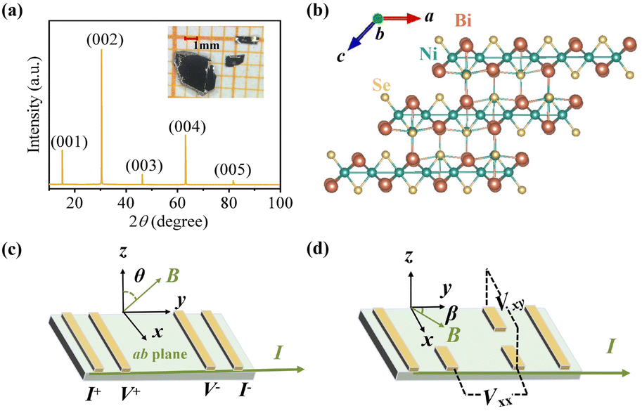 | ||
| Fig. 1 (a) The X-ray diffraction pattern of the Ni3Bi2Se2 crystal showing (00l) (l = integer) diffraction peaks, and the upper inset shows the optical image of the Ni3Bi2Se2 single crystal. (b) The schematic crystal structure of Ni3Bi2Se2. (c) The device configuration for out-of-plane transport measurement. (d) The schematic of the experimental configuration for the PHE and PAMR measurement. | ||
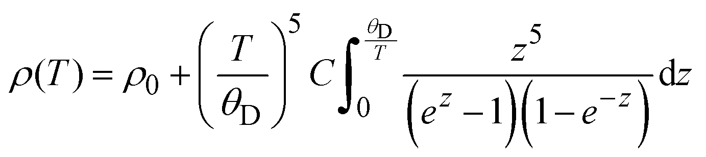
Angle-dependent out-of-plane (Fig. 1c) and in-plane (Fig. 1d) transport measurements were performed on a single crystal. Fig. 2a displays the temperature-dependent resistivity of the Ni3Bi2Se2 single crystal in the absence of a magnetic field. The resistivity shows metallic-like behaviour with a residual-resistance ratio (RRR) (ρ300K/ρ2K) of approximately 5, comparable to that observed in other parkerite-type compounds.37,38 This metallic-like behavior in topological insulators has been identified in several materials, such as TaSe3, CaBi2, and others, which is often attributed to the small energy gap.39–42 Quantitatively, the resistivity in the temperature range of 20–300 K can be accurately described using the Bloch–Grüneisen (BG) model (eqn (1)), as depicted by the red solid line in Fig. 2a. This suggests that electron–phonon interaction is the primary scattering mechanism:
 | (1) |
 | ||
| Fig. 2 (a) The temperature-dependent resistivity of the Ni3Bi2Se2 single crystal measured with the I‖ab plane. The red solid line indicates the fitting by the BG model for T ≥ 20 K. The inset shows the enlargement of low-temperature (2 K < T < 20 K) resistivity and the corresponding fitting. (b) The MR as a function of the magnetic field at different temperatures with I‖ab for the B⊥ab plane. (c) The magnetic field-dependent MR of the Ni3Bi2Se2 single crystal at different angles at 2 K. (d) The angle-dependent AMR at 2 K under different magnetic fields presented by a polar plot. (e) The magnetic field-dependent ordinary Hall resistivity at different temperatures. (f) The temperature-dependent carrier concentrations (nh and ne) and mobilities (μh and μe) were obtained from the two-band fitting. | ||
To explore the in-plane transport properties, we systematically rotated the crystal clockwise in the xy plane under various magnetic fields to induce the PHE and PAMR, respectively. The magnetic field and current were aligned parallel to the single crystal's ab plane, with the angle between the magnetic field and the current defined as β. It is important to note that the observed PHE curves could be a composite of the planar Hall signal and the ordinary Hall signal, due to the potential out-of-plane component of the magnetic field. We assessed the planar Hall resistivity under both positive and negative fields and determined the average data. Moreover, misalignment in the transverse Hall-bar setup can lead to the appearance of both in-plane and out-of-plane longitudinal resistivity components.13,47 Upon measuring several samples, we observed that the peaks and valleys of the PHE curves are positioned near 135°(315°) and 45°(225°), respectively, as shown in Fig. S4 (ESI†). This indicates that the contribution from the out-of-plane longitudinal resistivity component can be considered negligible. Furthermore, the in-plane longitudinal resistivity component can be ruled out using the formula [ρxy(β) + ρxy(π − β)]/2. In addition, the PHE and the PAMR phenomenon were repeatable for different samples, see Fig. S5 (ESI†).
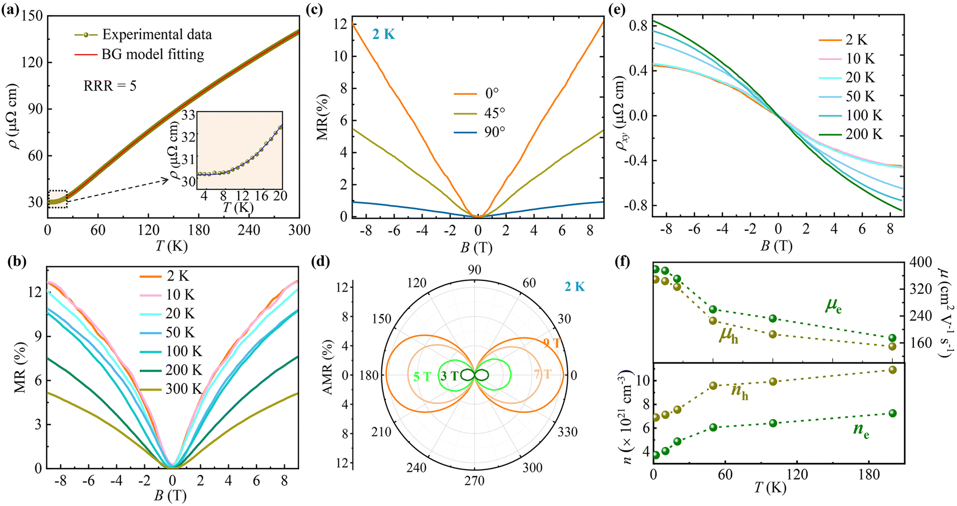
The angle-dependent intrinsic PHE under various magnetic fields is presented in Fig. 3a. It was observed that the PHE curve distinctly displays π periodicity with respect to the angle β. This behavior can be interpreted under the theory of the PHE:18,48
| ρPHExy = −Δρsinβcosβ | (2) |
 | ||
| Fig. 3 (a) The angle-dependent planar Hall resistivity and the corresponding fitting curves under different magnetic fields at 2 K. (b) The magnetic-field-dependent amplitude of the PHE extracted by fitting the curves in (a) via theoretical equations. (c) The PHE data and the corresponding fitting curves at various temperatures under 9 T. (d) The temperature-dependent amplitude of the PHE extracted from the fitted curves in (c). | ||
Indeed, several mechanisms, apart from the chiral anomaly,51 have been identified to contribute to the observed PHE, including anisotropic orbital magnetoresistance arising from Fermi pocket anisotropy, topological surface states characterized by spin-momentum locking,18,52,53 and anisotropic magnetic scattering.54 Given that Ni3Bi2Se2 is a non-magnetic material, the possibility of magnetic scattering contributing to the PHE can be excluded. Furthermore, the higher carrier density (Fig. 2f) suggests that the surface states of this material are likely submerged within the bulk, implying a minimal or even a negligible influence of topological surface states on its transport properties. The small or negligible topological surface states can also be reflected in the electronic band structure of Ni3Bi2Se2 (Fig. S6, ESI†). The bulk states with no global band gap and wide fluctuations will cover the surface state when projected the band structure onto the surface. At the same time, the DOS of the bulk state is far greater than the DOS of the surface state. Consequently, the origin of the PHE in this context requires further examination and clarification.
The angle-dependent in-plane resistivity under varying magnetic fields at 2 K is depicted in Fig. 4a. The in-plane resistivity adheres to a strict cos2β tendency with a period of π and can be accurately modeled using the equation provided (eqn (3)), as represented by the blue solid lines:
| ρxx = ρ⊥ − Δρcos2β | (3) |
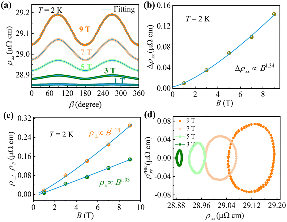 | ||
| Fig. 4 (a) The angle dependence of planar resistivity under different magnetic fields at T = 2 K. (b) Magnetic field dependence of resistivity amplitude extracted from the fitting curves in (a), and the solid curve is the power law fitting result. (c) Magnetic field dependence of ρ⊥ and ρ‖ at 2 K. The blue line represents the power law fitting results. (d) Parametric plots of the planar Hall resistivity and planar resistivity showing the orbits at 2 K. | ||
It has been observed that the resistivity gradually increases with increasing magnetic fields when B is parallel to I (β = 0° or 180°), a finding consistent with those presented in Fig. 2c and in contradiction to the NMR typically associated with the chiral anomaly. The obvious in-plane anisotropy in Ni3Bi2Se2 may be ascribed to the anisotropic Fermi surface induced by in-plane anisotropy of the crystal structure, as depicted in Fig. S7 (ESI†). The amplitudes of in-plane resistivity, extracted from Fig. 4a, are plotted as a function of the magnetic field in Fig. 4b and can be well-fitted by the relationship Δρxx ∝ B1.34. This is similar to the fitting results from the Δρyx − B curve (Fig. 3b), affirming the reliability of our measurements and analysis. Fig. 4c presents the parameters related to ρ‖ and ρ⊥ at 2 K, derived from the fitting results using eqn (3). For B parallel to I, ρ‖ exhibits a slight increase with an intensifying magnetic field. Conversely, a noticeable enhancement in ρ⊥ is observed when B is perpendicular to the I plane, indicating the potential presence of orbital magnetoresistance in the Ni3Bi2Se2 single crystal, primarily originating from the anisotropy of transport parameters such as effective mass, scattering time, and mobility.55
For a deeper analysis of the potential physical mechanism underlying the PHE signal, we plotted the amplitude of the PHE against the in-plane resistivity of the Ni3Bi2Se2 crystal under various magnetic fields and β as a parameter (Fig. 4d). The plots exhibit a “shock-wave” pattern and expand in the form of prolate ellipsoids towards larger resistivity values. Typically, in compounds where the pure chiral anomaly dominates, the orbit size increases more towards larger ρxx with an increasing magnetic field, due to the pumping of quasi-particles between Landau levels of opposite chirality. The parametric plot pattern usually displays concentric circles that expand uniformly with increasing fields due to the equilibrium effect of quasi-particle scattering between the charge and chiral pockets, observed in materials like GdPtBi, Na3Bi, etc.7 In the case of the anisotropic orbital magnetoresistance mechanism, when the magnetic field is in-plane, the orbit starts with a small ρxx and gradually expands to a larger ρxx with increasing magnetic fields, forming a shock wave shape. Thus, the shock-wave pattern observed in our sample further supports the hypothesis that the PHE may be attributed to anisotropic orbital magnetoresistance.
To date, while the PHE curves seem to align well with equations associated with the chiral anomaly, all indications, such as the absence of negative magnetoresistance and the shock wave pattern, suggest that the chiral anomaly does not primarily account for the PHE signal. Instead, anisotropic orbital magnetoresistance appears to play a significant role in the PHE observed in the Ni3Bi2Se2 single crystal. Additionally, Nandy et al. posited that the presence of surface-state transport in topological insulators is not a prerequisite for the occurrence of the PHE, which may instead be driven by the Berry curvature of the conduction band. To unequivocally ascertain the origin of the PHE signal, further studies are warranted. These should include the calculations of the electronic band structure, investigation of the morphology and anisotropy of the Fermi pockets in Ni3Bi2Se2, and experiments focusing on the PHE phenomenon in thin films of varying thicknesses and orientations.
Conclusions
In this study, we provide a comprehensive analysis of the transport properties of the topological insulator candidate Ni3Bi2Se2 single crystal. The ordinary Hall measurements highlight the simultaneous presence of both electrons and holes within the crystal. Furthermore, we observed a significant PHE and PAMR with a π period, occurring concurrently under coplanar electric and magnetic fields. The parametric plot reveals a shock-wave pattern, indicating that the observed PHE in Ni3Bi2Se2 primarily arises from in-plane orbital magnetoresistance, as opposed to the chiral anomaly typically associated with NMR. Our results lay the groundwork for further theoretical exploration of the PHE in topological insulators, which is crucial not only for uncovering new physical mechanisms but also for the development of potential applications.Author contributions
Yuzhe Ma: data curation, investigation, methodology, validation, and writing – original draft; Wen Sun: methodology and writing – review and editing; Qiunan Xu: methodology and formal analysis; Xinming Wang: methodology; Aisha Aqeel: methodology and writing – review and editing; Guowei Li: conceptualization, supervision, funding acquisition, and writing – review and editing.Data availability
The data supporting this article have been included as part of the ESI.†Conflicts of interest
There are no conflicts to declare.Acknowledgements
This work was financially supported by the National Natural Science Foundation of China (52271194), the Ningbo Yongjiang Talent Introduction Programme (2022A-090-G), and the Hundred Talents Programs in the Chinese Academy of Science. G. Li thanks for the support from the Max Planck Partner Group program.References
- H. X. Tang, R. K. Kawakami, D. D. Awschalom and M. L. Roukes, Phys. Rev. Lett., 2003, 90, 107201 CrossRef CAS PubMed.
- L. Fina, X. Marti, D. Yi, J. Liu, J. H. Chu, C. Rayan-Serrao, S. Suresha, A. B. Shick, J. Zelezny, T. Jungwirth, J. Fontcuberta and R. Ramesh, Nat. Commun., 2014, 5, 4671 CrossRef PubMed.
- J. Zhou, W. Zhang, Y.-C. Lin, J. Cao, Y. Zhou, W. Jiang, H. Du, B. Tang, J. Shi, B. Jiang, X. Cao, B. Lin, Q. Fu, C. Zhu, W. Guo, Y. Huang, Y. Yao, S. S. P. Parkin, J. Zhou, Y. Gao, Y. Wang, Y. Hou, Y. Yao, K. Suenaga, X. Wu and Z. Liu, Nature, 2022, 611, E1 CrossRef CAS PubMed.
- W. Ai, F. Chen, Z. Liu, X. Yuan, L. Zhang, Y. He, X. Dong, H. Fu, F. Luo, M. Deng, R. Wang and J. Wu, Nat. Commun., 2024, 15, 1259 CrossRef CAS PubMed.
- J. Xiong, S. K. Kushwaha, T. Liang, J. W. Krizan, M. Hirschberger, W. Wang, R. J. Cava and N. P. Ong, Science, 2015, 350, 413–416 CrossRef CAS PubMed.
- X. Huang, L. Zhao, Y. Long, P. Wang, D. Chen, Z. Yang, H. Liang, M. Xue, H. Weng, Z. Fang, X. Dai and G. Chen, Phys. Rev. X, 2015, 5, 031023 Search PubMed.
- S. Liang, J. Lin, S. Kushwaha, J. Xing, N. Ni, R. J. Cava and N. P. Ong, Phys. Rev. X, 2018, 8, 031002 CAS.
- S. Nandy, G. Sharma, A. Taraphder and S. Tewari, Phys. Rev. Lett., 2017, 119, 176804 CrossRef CAS PubMed.
- H. Li, H.-W. Wang, H. He, J. Wang and S.-Q. Shen, Phys. Rev. B, 2018, 97, 201110 CrossRef CAS.
- P. Li, C. Zhang, Y. Wen, L. Cheng, G. Nichols, D. G. Cory, G.-X. Miao and X.-X. Zhang, Phys. Rev. B, 2019, 100, 205128 CrossRef CAS.
- Q. Liu, F. Fei, B. Chen, X. Bo, B. Wei, S. Zhang, M. Zhang, F. Xie, M. Naveed, X. Wan, F. Song and B. Wang, Phys. Rev. B, 2019, 99, 155119 CrossRef CAS.
- P. Li, C. H. Zhang, J. W. Zhang, Y. Wen and X. X. Zhang, Phys. Rev. B, 2018, 98, 121108 CrossRef CAS.
- R. Singha, S. Roy, A. Pariari, B. Satpati and P. Mandal, Phys. Rev. B, 2018, 98, 035110 CrossRef.
- L. M. Schoop, M. N. Ali, C. Strasser, A. Topp, A. Varykhalov, D. Marchenko, V. Duppel, S. S. Parkin, B. V. Lotsch and C. R. Ast, Nat. Commun., 2016, 7, 11696 CrossRef CAS PubMed.
- L. M. Schoop, F. Pielnhofer and B. V. Lotsch, Chem. Mater., 2018, 30, 3155–3176 CrossRef CAS.
- A. A. Taskin, H. F. Legg, F. Yang, S. Sasaki, Y. Kanai, K. Matsumoto, A. Rosch and Y. Ando, Nat. Commun., 2017, 8, 1340 CrossRef CAS PubMed.
- S.-H. Zheng, H.-J. Duan, J.-K. Wang, J.-Y. Li, M.-X. Deng and R.-Q. Wang, Phys. Rev. B, 2020, 101, 041408 CrossRef CAS.
- S. Nandy, A. Taraphder and S. Tewari, Sci. Rep., 2018, 8, 14983 CrossRef CAS PubMed.
- B. Wu, X.-C. Pan, W. Wu, F. Fei, B. Chen, Q. Liu, H. Bu, L. Cao, F. Song and B. Wang, Appl. Phys. Lett., 2018, 113, 011902 CrossRef.
- D. F. Liu, A. J. Liang, E. K. Liu, Q. N. Xu, Y. W. Li, C. Chen, D. Pei, W. J. Shi, S. K. Mo, P. Dudin, T. Kim, C. Cacho, G. Li, Y. Sun, L. X. Yang, Z. K. Liu, S. S. P. Parkin, C. Felser and Y. L. Chen, Science, 2019, 365, 1282 CrossRef CAS PubMed.
- E. Liu, Y. Sun, N. Kumar, L. Muechler, A. Sun, L. Jiao, S.-Y. Yang, D. Liu, A. Liang, Q. Xu, J. Kroder, V. Suess, H. Borrmann, C. Shekhar, Z. Wang, C. Xi, W. Wang, W. Schnelle, S. Wirth, Y. Chen, S. T. B. Goennenwein and C. Felser, Nat. Phys., 2018, 14, 1125 Search PubMed.
- Shama, R. K. Gopal and Y. Singh, J. Magn. Magn. Mater., 2020, 502, 166547 CrossRef CAS.
- S.-Y. Yang, J. Noky, J. Gayles, F. K. Dejene, Y. Sun, M. Dorr, Y. Skourski, C. Felser, M. N. Ali, E. Liu and S. S. P. Parkin, Nano Lett., 2020, 20, 7860–7867 CrossRef CAS PubMed.
- T. Zhang, T. Yilmaz, E. Vescovo, H. X. Li, R. G. Moore, H. N. Lee, H. Miao, S. Murakami and M. A. McGuire, npj Comput. Mater., 2022, 8, 2201 Search PubMed.
- H. Fang, M. Lyu, H. Su, J. Yuan, Y. Li, L. Xu, S. Liu, L. Wei, X. Liu, H. Yang, Q. Yao, M. Wang, Y. Guo, W. Shi, Y. Chen, E. Liu and Z. Liu, Sci. China Mater., 2023, 66, 2032–2038 CrossRef CAS.
- Shama, R. K. Gopal, G. Sheet and Y. Singh, Sci. Rep., 2021, 11, 12618 CrossRef CAS PubMed.
- T. Sakamoto, M. Wakeshima and Y. Hinatsu, J. Condens. Matter Phys., 2006, 18, 4417–4426 CrossRef CAS PubMed.
- M. G. Vergniory, L. Elcoro, C. Felser, N. Regnault, B. A. Bernevig and Z. Wang, Nature, 2019, 566, 480–485 CrossRef CAS PubMed.
- T. Zhang, Y. Jiang, Z. Song, H. Huang, Y. He, Z. Fang, H. Weng and C. Fang, Nature, 2019, 566, 475–479 CrossRef CAS PubMed.
- D. Xiao, M.-C. Chang and Q. Niu, Rev. Mod. Phys., 2010, 82, 1959 CrossRef CAS.
- S. Wang, P. Zhang, C. Ren, H. Tian, J. Pang, C. Song and M. Sun, J. Supercond. Novel Magn., 2019, 32, 2947–2957 CrossRef CAS.
- P. C. Canfield, T. Kong, U. S. Kaluarachchi and N. H. Jo, Philos. Mag., 2016, 96, 84–92 CrossRef CAS.
- P. C. Canfield, Rep. Prog. Phys., 2020, 83, 016501 CrossRef CAS PubMed.
- X.-L. Chen, J.-K. Liang and C. Wang, Acta Phys. Sin., 1995, 4, 259 CAS.
- G. M. Sheldrick, Acta Crystallogr., Sect. C: Struct. Chem., 2015, 71(1), 3–8 Search PubMed.
- G. Kresse and J. Furthmüller, Phys. Rev. B: Condens. Matter Mater. Phys., 1996, 54, 11169 CrossRef CAS PubMed.
- T. Sakamoto, M. Wakeshima, Y. Hinatsu and K. Matsuhira, Phys. Rev. B: Condens. Matter Mater. Phys., 2007, 75, 060503 CrossRef.
- Z. Y. Zhang, M. Ikeda, M. Utsumi, Y. Yamamoto, H. Goto, R. Eguchi, Y. F. Liao, H. Ishii, Y. Takabayashi, K. Hayashi, R. Kondo, T. C. Kobayashi and Y. Kubozono, Inorg. Chem., 2024, 63, 2553–2561 CrossRef CAS PubMed.
- S. Nie, L. Xing, R. Jin, W. Xie, Z. Wang and F. B. Prinz, Phys. Rev. B, 2018, 98, 125143 CrossRef CAS.
- W. Xia, X. Shi, Y. Zhang, H. Su, Q. Wang, L. Ding, L. Chen, X. Wang, Z. Zou, N. Yu, L. Pi, Y. Hao, B. Li, Z. Zhu, W. Zhao, X. Kou and Y. Guo, Phys. Rev. B, 2020, 101, 155117 CrossRef CAS.
- Q. Jiang, D. Wang, Z. Liu, Z. Jiang, H. Qian, X. Shen, A. Li, D. Shen, S. Qiao and M. Ye, Phys. Rev. B, 2021, 104, 245112 CrossRef CAS.
- Y. Ma, Y. Wang and G. Wang, Phys. Scr., 2023, 98, 015002 CrossRef CAS.
- J. M. Ziman, Electrons and Phonons: The Theory of Transport Phenomena in Solids, Oxford University Press, 2001 Search PubMed.
- Y. Ma, Y. Wang and G. Wang, EPL, 2022, 138, 36003 CrossRef CAS.
- S. Sasmal, R. Mondal, R. Kulkarni, A. Thamizhavel and B. Singh, J. Condens. Matter Phys., 2020, 32, 335701 CrossRef CAS PubMed.
- Z. Hou, Y. Wang, E. Liu, H. Zhang, W. Wang and G. Wu, Appl. Phys. Lett., 2015, 107, 202103 CrossRef.
- H. Li, H.-W. Wang, H. He, J. Wang and S.-Q. Shen, Phys. Rev. B, 2018, 97, 201110(R) CrossRef.
- M. Wu, D. Tu, Y. Nie, S. Miao, W. Gao, Y. Han, X. Zhu, J. Zhou, W. Ning and M. Tian, Nano Lett., 2022, 22, 73–80 CrossRef CAS PubMed.
- N. Zhang, G. Zhao, L. Li, P. Wang, L. Xie, B. Cheng, H. Li, Z. Lin, C. Xi, J. Ke, M. Yang, J. He, Z. Sun, Z. Wang, Z. Zhang and C. Zeng, Proc. Natl. Acad. Sci. U. S. A., 2020, 117, 11337–11343 CrossRef CAS PubMed.
- A. A. Burkov, Phys. Rev. B, 2017, 96, 041110(R) CrossRef.
- S. Liang, J. Lin, S. Kushwaha, J. Xing, N. Ni, R. J. Cava and N. P. Ong, Phys. Rev. X, 2018, 8, 031002 CAS.
- A. Sulaev, M. Zeng, S.-Q. Shen, S. K. Cho, W. G. Zhu, Y. P. Feng, S. V. Eremeev, Y. Kawazoe, L. Shen and L. Wang, Nano Lett., 2015, 15(3), 2061–2066 CrossRef CAS PubMed.
- W. Rao, Y.-L. Zhou, Y.-J. Wu, H.-J. Duan, M.-X. Deng and R.-Q. Wang, Phys. Rev. B, 2021, 103, 155415 CrossRef CAS.
- H. X. Tang, R. K. Kawakami, D. D. Awschalom and M. L. Roukes, Phys. Rev. Lett., 2003, 90, 107201 CrossRef CAS PubMed.
- S. Roy, R. Singha, A. Ghosh and P. Mandal, Phys. Rev. Mater., 2021, 5, 064203 CrossRef CAS.
Footnote |
| † Electronic supplementary information (ESI) available: Fig. S1–S7: EDX spectrum and elemental mapping images, XPS spectra, ordinary Hall resistivity, planar Hall resistivity, the electronic band structure and the schematic single crystal of Ni3Bi2Se2. Tables S1–S6: the parities for each time reversal invariant momentum, crystallographic data, and EDX experimental data in Ni3Bi2Se2 single crystal. CCDC 2367489. For ESI and crystallographic data in CIF or other electronic format see DOI: https://doi.org/10.1039/d4tc01382d |
| This journal is © The Royal Society of Chemistry 2024 |