
 Open Access Article
 This Open Access Article is licensed under a
 Creative Commons Attribution 3.0 Unported Licence
Infiltration issues in printed mesoporous carbon perovskite solar cells: a troubleshooting guide
C. A.
Worsley
 *,
T.
Dunlop
,
S. J.
Potts
,
R.
Bolton
,
E.
Jewell
and
T. M.
Watson
*
*,
T.
Dunlop
,
S. J.
Potts
,
R.
Bolton
,
E.
Jewell
and
T. M.
Watson
*
Swansea University, Fabian way, Neath, SA18EN, Northern Ireland, UK. E-mail: c.a.worsley@swansea.ac.uk; t.m.watson@swansea.ac.uk
First published on 24th May 2024
Abstract
Printed mesoscopic carbon perovskite solar cells (CPSCs) represent a potential frontrunner to perovskite commercialisation due to their inherent stability and easily scaled fabrication methods. Devices consist of three screen printed mesoporous layers of TiO2, ZrO2 and carbon, which are subsequently infiltrated with perovskite. It is well established that complete infiltration, or filling, of the base TiO2 layer is key to achieving peak performance and reproducibility in both lab-scale devices and modules. A thorough understanding of the factors influencing infiltration is therefore essential for both lab-scale research and scale-up. TiO2 infiltration is easily examined by optical microscopy through the glass substrate. This work identifies common characteristic infiltration defects at multiple scales, caused by specific issues in the manufacturing process such as mesh marking, printing issues, contaminant damage and environmental fluctuations. Likely causes and potential solutions are presented for each type of defect, to produce a troubleshooting reference resource for tackling this problem at multiple scales. This should help enhance lab-scale reproducibility providing a simple method for quality control in future large-scale ventures.
Introduction
Since their advent in 2009, perovskite solar cells have quickly evolved to produce champion PCEs of 25.6%, surpassing that of many commercially available silicon modules.1,2 Amenable to solution-based processing, perovskites therefore represent an exciting opportunity for developing low-cost thin film photovoltaics.However, champion efficiencies are generally attained at small scale and achieved using non-scalable techniques such as spin coating.2 Additionally, devices are prone to degradation on exposure to light, water, and oxygen.3–5 This is particularly pertinent in the case of high-performance planar devices, which frequently rely on expensive and unstable hole transport materials such as SPIRO-OMeTAD to achieve peak performance.6,7
Mesoporous carbon perovskite solar cells (CPSCs) represent a more stable, scalable alternative to planar architectures. Despite historically exhibiting much lower PCEs than planar architectures, champion device performance has risen dramatically in recent years to a record of 19%.8,9
Devices consist of three screen printed mesoporous layers of TiO2, ZrO2 and carbon, which are subsequently infiltrated with perovskite precursor.10 The lack of an expensive organic hole transport material reduces the manufacturing cost and improves stability, which is further enhanced by the thick hydrophobic carbon back electrode.11,12 Incorporating 4-aminovaleric acid, which passivates surface defects and inhibits MAI loss by sitting at grain boundaries has enabled these devices to pass stringent IEC61215:2016 standards, highlighting their resilience under environmental stress.13–15
However, perhaps the main advantage of these cells is the ease of large-scale fabrication. Screen printing is already industrially available at multiple scales using relatively low-cost equipment.16 As such, 220 cm2 active area modules of over 9% PCE have already been presented in the literature.17
One of the key requirements for producing high-performing CPSCs is achieving complete infiltration, or filling, of the base TiO2 layer.18–21 Unfilled, perovskite free voids at the base of the stack represent areas of poor perovskite–electrode contact, producing low currents and limited charge extraction, as well as reducing light absorption.18,21 Stability is also impacted, as poor stack filling has been linked with high defect density, producing increased recombination and decreased lifetime.18–20
Infiltration issues can present at multiple scales, from visually obvious defects to micron-scale voids. Even devices that appear uniform to the naked eye may therefore present differently once examined with a microscope. Recent work quantified the base infiltration of TiO2 layers using optical microscopy and paired image analysis, to find that the proportion of uninfiltrated TiO2 strongly correlated with performance.22 This quick and non-destructive method could therefore be used for PCE prediction of devices or modules.
Determining the root cause of poor infiltration can be extremely complex. Devices are usually fabricated in ambient conditions and infiltration is influenced by many different factors, including solvent viscosity, crystallisation time, and layer roughness.17 As such, inter-batch variations are often blamed on the ambient nature of the fabrication process. Developing a thorough understanding of the causes and presentation of different types of infiltration defect will allow for targeted problem solving upon experiencing these issues.
This work presents common characteristic infiltration defects observed in CPSCs. The presentation and likely cause of each problem is discussed, and potential methods for remedying each issue are identified, with the aim of producing a reference resource of methods for targeting these problems in both lab-scale devices and modules. Linked with specific manufacturing issues, each defect type can be reduced or prevented by addressing problems in the fabrication process. This should help both researchers and future scaled initiatives in achieving more reproducible infiltration and performance.
Results and discussion
This work will present several characteristic infiltration problems commonly observed in CPSCs along with their likely cause and potential solutions. It should be noted that although discussion will be mostly in the context of devices, the causes and solutions presented are equally applicable to modules.For quick identification of problems, Fig. 1 shows a diagrammatic representation of identified common, characteristic infiltration defects observed at the micro (blue) and macro (green) scale in CPSCs, alongside checks for potential causes. Each issue will be discussed in greater detail in a following subsection, with a final section covering causes of low performance in the absence of defects.
 | ||
| Fig. 1 Diagrams of common large (green text box, (iii)–(v)) and small-scale (blue text box, (i), (ii) and (vi)) infiltration issues in cells and modules, alongside likely causes and suggested checks. Each defect is discussed seperately in the relevant numbered section below. | ||
Note that each defect type can appear at a range of scales, and poorly infiltrated devices often exhibit many defects – sometimes with a combination of many types. The specific impact on device performance will therefore be highly dependent on defect size, spread, and prevalence. The effect on performance may also vary depending on perovskite formulation. Thus, it is not possible to provide a representative or accurate value for the performance increase attained by removing a given defect type, as its negative impact will be different in each cell. Specific performance data is not therefore presented in this work, instead focusing on the specific manufacturing issues that cause these characteristic defects and how to overcome them.
Recent work has found that device performance is intrinsically linked to the proportion of uninfiltrated, perovskite free TiO2 observable through the glass substrate, where it was found that even a small increase in uninfiltrated area from 0.16% to 1.17% reduced PCE from 14.88% to 12.36%.22 Critically, PCE losses increased more drastically as uninfiltrated area increased.
Therefore, should readers wish to predict or compare the potential detrimental impact of a given defect type in their unique device or module, optical examination of the uninfiltrated area produced by each defect type could be employed. This can be done through qualitative examination, or quantitatively using image analysis.22 Note that the specific effect of uninfiltrated area (and thus a given defect) on performance may vary with perovskite precursor formulation, stack composition, or layer thicknesses.
Issue (i) contamination
Often (but not always) visible at the macro-scale, contaminants and solvent damage produce similar issues in completed devices, producing uneven defects of varied size, sometimes with a distinctive ‘halo’ or ringed surrounding pattern (Fig. 2). In the case of physical contaminants, a particle can be present at the defect centre, whereas solvent contamination issues are particle free. Particles will be visible through the glass substrate if the associated contamination is under, in, or on the TiO2 print. Particle contamination of the ZrO2 and carbon may also result in defects, but the given particle is unlikely to be visible through the glass substrate. | ||
| Fig. 2 Optical images of infiltration defects caused by solvent droplet damage and particle contamination. | ||
While solvent damage can be easily prevented through careful handling of liquids around printed stacks (especially when wet), physical contamination can be more persistent depending on the source. Wet and dry printed layers, screens and printing equipment should all be stored under covers to protect from dust and other airborne particulates. Placing wet films in areas of high airflow is not advised, as it can prevent film settling/slumping and increase the likelihood of particle contamination.
Upon observing these defects in cells or modules, pastes, screens, and printing equipment should be carefully inspected for particles or blockages. Blocked screens require cleaning, while contaminated pastes should be disposed of. If equipment and materials appear clean, the printing, film relaxation/slumping, annealing and storage areas should be wiped down to eliminate the source of particles, and storage procedures reviewed where necessary.
Issue (ii) micron sized, evenly spaced defects
Perhaps the most characteristic defects are those caused by mesh marks; troughs or peaks at the surface of a screen printed layer. Mesh marks occur due to ink filaments forming at mesh crossover sections as the screen separates from the substrate during printing. This produces round, evenly spaced infiltration defects in the finished device. Usually present across a large area, these features are obvious when examining the infiltrated TiO2 layer with an optical microscope (Fig. 3a–c). Critically, mesh marks in the ZrO2 or carbon print can cause infiltration defects at the base of the TiO2. (Fig. 3a–c) shows optical microcopy images of infiltrated TiO2 layers from three devices, which respectively show evidence of TiO2, ZrO2 and carbon related mesh mark infiltration defects. | ||
| Fig. 3 Optical images of infiltrated TiO2 in devices showing mesh mark defects from (a) TiO2, (b) ZrO2, and (c) carbon screens. (d)–(f) Show diagrams of mesh dimensions of TiO2, ZrO2 and carbon screens respectively, with circles representing cross sections where an infiltration issue is present in the device. (g) Shows mesh types and calculated gap size for each layer. | ||
As presented in Fig. 3, observed infiltration defects will correspond with the mesh dimensions of the relevant screen. Therefore, if different screens have been used for TiO2, ZrO2 and carbon, defect spacing can be measured to conclude in which layer the problematic marks reside. For example, the small defects in Fig. 3a must correspond with those from the TiO2 layer, as this was the only deposition where a fine mesh was used (Fig. 3c). Note that defects may only appear (or be more severe) at alternate cross sections, as is the case in Fig. 3b and c. If similar mesh screens are used for different layers, the problematic layer can be identified using WLI (white light interferometry) of any remaining uninfiltrated devices single prints (Fig. 3b).
Crucially, marks in a given layer are not necessarily due to printer setup issues in that layer. For example, it has been shown that slight increases in ZrO2 roughness can cause severe increases in marking of the subsequent carbon print.22 Therefore, the topology of all layers (in an uninfiltrated sample) should be examined upon observing mesh marking to ascertain the root cause of the problem.
As mesh marks are caused by ink filamentation during printing, printer setup and ink formulation are critical to their prevention. Printer setup techniques to avoid mesh marking include using the minimum printable squeegee pressure or switching to a finer mesh.22,23 It should be noted that not all pastes are suitable for fine mesh screens- for example, the large graphite flakes in carbon inks are likely to cause blockages. A flow coat print regime, where paste is spread over the screen before a single squeegee pass can also reduce marking. Unless pastes are considerably viscous, a print–print (or two squeegee passes) is not likely required and unnecessarily increases the risk of severe marking.22,23 Alternatively, pastes can be altered to reduce filamentation by lowering viscosity and/or elasticity.23 This can be achieved with careful dilution or by changing the amount or type of binders used.22
To avoid any detriment to device performance, film thickness and topography should be checked after any alteration to printer setup, regime, or ink formulation.
Issue (iii) gradient infiltration
Clear colour intensity gradients across the active area are indicative of printing inconsistencies such as uneven thickness or topology. Print variation in any layer can produce infiltration issues, although the thicker ZrO2 and carbon are more likely to cause problems, as precursor must travel further to penetrate these films. This can occur across the width of a single cell or module, or across several cells when printing small-scale devices. Such films then cause large performance variations within a batch of cells, or decreased power output and performance in a module.Sub-optimal printer setup is usually the cause of these issues, although glass warping can also cause similar problems. Consequently, it may be a more prevalent issue in more manual screen-printing equipment, as advanced machines will be able to detect screen, squeegee or substrate misalignment. As shown in Fig. 4a, uneven squeegee or flow coat setup can produce thickness variation across the print. In extreme cases, one side of the print will be extremely thick (limiting infiltration), and the other thin with pronounced mesh marking (as depicted in Fig. 4a). Note that small inconsistencies in the ZrO2 can cause large problems in the subsequent carbon print, so sub-optimal inhomogeneous carbon prints may not be a consequence of printer setup during carbon deposition.22
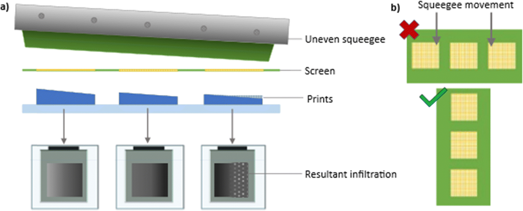 | ||
| Fig. 4 (a) Diagrammatic representation of the consequences of uneven squeegee pressure and its resultant impact on device infiltration. Note that mesh marking defects in real samples will only be visible via optical microscopy. (b) Screen alignment to limit horizontal print variations. | ||
In the case of glass warping, observed infiltration gradients will align with the substrate warp, with areas further from the screen usually producing thicker prints, and areas closer to the screen producing thinner ones (sometimes accompanied by mesh marking).
It is advisable to retain an uninfiltrated device stack from each print batch, as print thicknesses or substrate warp can be then examined with profilometry, while white light interferometry provides quick topological data. Infiltrated devices are more difficult: although mesh marking problems can be observed through the glass substrate, cross sectional analysis may be required to examine thickness across the printed layer.
Careful setup and pressure monitoring can help prevent squeegee related issues. Changing screen designs to limit the horizontal print width (depicted in Fig. 4b) can also improve uniformity and batch variation. In the case of glass warping, ramped heating and cooling steps for blocking layer spraying and each high temperature anneal can help minimise these issues.
Issue (iv) extreme infiltration variation between cells in a single print batch, not linked to position on the print bed/large grey or yellow areas in otherwise well infiltrated modules.
Crystallisation speed is well documented to impact infiltration, with longer crystallisation times having been found to improve the infiltration of perovskite precursors based on a variety of solvents. This means that inconsistencies in temperature or airflow during infiltration or annealing can produce very different infiltration depending on the position of the device on the hot plate or oven (Fig. 5a and b). This is the case even where the print quality is consistent across the batch or module. Unless care is taken to note the hot plate position of each device during annealing, the infiltration variation across a batch may appear random. It is therefore advisable to examine each device upon removal from the hot plate or oven after annealing and note the position of any which exhibit obvious infiltration issues. | ||
| Fig. 5 Diagrammatic representation of (a) an unevenly heating hot plate and (b) resultant impact on device infiltration. Depicted in (c) is a photograph of damage on a 30 × 30 cm2 module caused by heating elements and airflow during perovskite annealing. | ||
This issue can occur at multiple scales and using different equipment setup. For example, Fig. 5c shows a 30 × 30 cm2 module annealed on a conveyor dryer. Through the glass substrate, greyish white and yellow defects can be seen, impacting multiple cells. The grey or white perovskite free voids indicate an infiltration issue caused by fast crystallisation and high airflow, whereas the yellow areas show accelerated degradation due to uneven heating. On examination of equipment, the yellow defects corresponded with overhead heating elements in the dryer and the white and grey with areas of high airflow.
A simple partial cover was thus applied, to protect the module surface while allowing sufficient solvent removal. This completely eliminated the defects, as shown in Fig. 6.
 | ||
| Fig. 6 Photographs of 519 cm2 active area modules with (RHS) and without (LHS) a cover during perovskite annealing. (i) Back electrode, (ii) through glass substrate, (iii) magnified with applied colour filter to highlight infiltration problems. | ||
Issues (v) and (vi) random void or crystallite spacing at micro or macro-scale
Perhaps the most difficult to diagnose is when devices present with apparently random infiltration issues spread. As shown in Fig. 7a, this can appear at multiple scales with extreme variation in the shape and distribution of observed defects. | ||
| Fig. 7 (a) Optical microscopy images of randomly distributed infiltration defects at different scales. (b) Diagrammatic representation and example photograph of (i) impeded infiltration and (ii) preferential surface growth. (c) The impact of crystallisation speed with each mechanism. | ||
There exist two distinct mechanisms that can cause these problems, depicted in Fig. 7b. Impeded infiltration (Fig. 7b(i)) occurs when precursor cannot effectively reach the base of the stack, while preferential surface growth (Fig. 7b(ii)) is seen when nucleation and crystal growth occurs more favourably atop or within the carbon layer, reducing crystal formation in the small pores of the TiO2 electrode. Both mechanisms can also occur concurrently: e.g. upon applying a new precursor formulation that favours surface crystal growth to a batch of cells with thick, rough carbon prints.
Example photographs of devices with particularly severe infiltration issues caused by each mechanism are shown in Fig. 7b. It should be noted that although the devices in the example look very different, they are not characteristic of the associated infiltration issue: without further examination or specific knowledge of the given sample, is not possible to tell visually which mechanism is present.
The causative mechanism can sometimes be identified through monitoring perovskite crystallisation speed across a batch and subsequently examining infiltration. To induce different crystallisation speeds, samples can be deliberately annealed at different temperatures. In the case of impeded infiltration, the best infiltration will be attained in devices that crystallised slowly, as the precursor had more time to percolate the stack. Conversely, with preferential surface growth the best infiltration will present in rapidly crystallised devices, as the infiltrated precursor rapidly forms small grains within the TiO2 pores instead of slowly growing larger grains at the carbon electrode. If both issues are present, crystallisation speed will likely have little impact on infiltration.
Impeded infiltration can be caused by anything that can restrict the flow of precursor through the stack. This includes increased print roughness or thickness, horizontal graphite flake alignment, insufficient binder removal during annealing and increased precursor viscosity. The problem can then be exacerbated by suboptimal annealing conditions such as high temperatures or surface airflow.
Severe issues are usually caused by multiple concurrent problems acting in tandem. Fig. 8 shows images of TiO2 infiltration from two devices from the same print batch, (a) annealed on the hot plate and (b) under a partial cover to limit surface airflow. Reducing surface airflow has produced better infiltration in sample b, revealing mesh marking defects that were not observable in the more sparsely filled sample a. Both issues (high surface airflow and mesh marking) therefore require resolving to ensure high-quality infiltration.
 | ||
| Fig. 8 Optical microscopy images of two devices with impeded infiltration, (a) annealed on an open hot plate and (b) under a partial cover. (b) Reveals mesh marks not observed. | ||
To help resolve severe impeded infiltration, the following steps can be taken:
• Consider depositing a larger volume of perovskite precursor to increase the overall crystallisation time.
• Examine the annealing environment for potential exposure of samples to high airflow or high temperature. Partial covers can reduce surface airflow, and lower annealing temperatures may assist infiltration. If a solvent is poorly wetting or particularly viscous, a specially designed cover may be necessary to achieve acceptable infiltration.24
• Examine any better infiltrated areas for evidence of problems such as mesh marking. Minor mesh marking (especially in the TiO2 layer) should not cause extreme infiltration issues by itself, so evidence of this any layer is unlikely to be the sole cause.
• Check any uninfiltrated prints for defects such as increased layer roughness or extreme thickness. If no uninfiltrated stacks from the relevant printing batches remain, cross sectional imaging may provide some insight into layer thickness or roughness.
• Place carbon prints directly on the hot plate after printing and infiltrate precursor directly after annealing the carbon layer to minimize horizontal settling of graphite plates.
• Consider methods to reduce precursor viscosity or improve wetting. This could entail heating the precursor, incorporating a solvent additive, or reducing precursor concentration. Bear in mind that heating can induce precipitation in some precursors, and so is not always a suitable method.25
Preferential surface growth is more associated with the perovskite precursor itself. Changes in formulation that limit nucleation and favour large grain growth, such as introducing highly coordinating precursor solvents may therefore produce this problem. Poorly dissolved or precipitated precursors may also induce surface growth, with undissolved particulates or precipitated crystallites deposited atop the stack acting as nucleation sites.
To help resolve preferential surface growth, the following methods can be trialled:
• Consider depositing a smaller amount of precursor, to limit the amount at the device surface.
• Replace top-down drop casting with edge infiltration, depositing precursor at the ZrO2 edges and allowing capillary action to drive device filling.
• Consider molecular additives that promote nucleation within the stack, such as 5-aminovaleric acid. Note that additives can slow device response times and limit grain size.13,26,27
• Some work has shown that applying highly optimised covers extremely close (∼50 μm from the cell surface) can promote crystal growth within the stack, as the resultant high concentration of solvent vapour at the cell surface prevents surface growth. Note that such annealing processes are extremely long (∼20 hours) and can have extremely narrow processing windows.28
The impact of these changes will be highly dependent on the precise precursor formulation and device structure, and effectiveness may therefore be highly variable. A universal solution for preventing this infiltration issue in all CPSCs cannot therefore be presented.
Issue (vii) performance drops and hysteresis changes without infiltration problems
Upon experiencing benchmark performance drops without obvious infiltration issues, layer thickness in the relevant print batch should be examined. Sub optimally thin ZrO2 layers can lower benchmark performance and dramatically increase hysteresis, although it should be noted that the optimal ZrO2 thickness may vary depending on the perovskite composition.29–31Carbon layers are optimally of 10–20 μm thickness.32–34 Thin (<10 μm) carbon layers or blocking layers can cause overall benchmark performance losses as thinner layers are more resistive, and resultant devices suffer from poor charge extraction and increased recombination.32–34 Optimal blocking layer thickness is approximately 30 nm.34 Note that excessively thick (>75 nm) blocking layers can also cause extraction issues, with devices presenting a high shunt resistance.34
If any uninfiltrated samples remain, ZrO2 and carbon thickness can be examined with profilometry. Ideally, uninfiltrated samples should have a dried (i.e. not annealed) carbon layer for any thickness measurements. This is because the carbon layer post-annealing is mechanically fragile and easily damaged by profilometry or cross-sectional sample preparation. If only infiltrated samples are available, cross-sectional SEM is required.
Summary table
To aid in fast defect identification and prevention, a summary table is provided below. Defect types, scale and causes are highlighted alongside potential checks and solutions (Table 1).| Issue | Example | Scale | Cause | What to check | Potential solutions |
|---|---|---|---|---|---|
| Particle/solvent damage. |

|
Depends on the size of the particle/droplet. | Particle contaminant or solvent damage. | • Inspect paste, equipment, and storage areas for contamination. | • Replace bad paste, clean equipment, printing, slumping and storage areas. |
| • Droplet damage has no central particle. | • Ensure substrates are particle free before printing. | ||||
| • Cover prints when slumping and annealing. | |||||
| Mesh marking. |

|
Depends on screen mesh spacing and thread widths. | Filamentation during printing. Could be due to rough print in the layer below. | • Spacing corresponds with thread spacing of the relevant screen. May only appear at 2x spacing. | • Print using minimum effective squeegee pressure. |
| • Marks/roughness on affected print and the one underneath (WLI recommended). | • Trial a flow coat method. | ||||
| • Trial a finer mesh screen (may need multiple layers). | |||||
| • Slight dilution of very viscous pastes. | |||||
| Gradient infiltration. |

|
Macro-scale (mm–cm), across cell or module width/length. | Uneven printer setup or substrate warping. | • Printer setup. | • Careful printer setup. |
| • Glass substrate warping (profilometry recommended). | • Regularly change squeegees to minimise wear. | ||||
| • Reduce warp with slower ramps to all heating/cooling steps. | |||||
| Large module patches/extreme variation within a device batch. |

|
Scale variable, generally mm to cm. | Uneven heating or airflow during perovskite annealing/infiltration. | • If defects correspond to position on print bed, check printer setup. | • Ensure full binder removal during stack anneals. If unsure on removal temperatures, perform a TGA. |
| Incomplete binder removal. | • Check that paste and perovskite annealing hot plates/ovens are consistent and accurate. | • Apply a partial cover during perovskite annealing (limit airflow and protect from top-down heating elements). | |||
| • Prevent high airflow during perovskite annealing. | |||||
| Random void or crystal spacing. |

|
Very variable in scale and shape. | (i) Impeded infiltration. | • Does faster perovskite crystallisation reduce infiltration? | • Reduce perovskite annealing temperature or increase infiltration volume. |
| Well infiltrated sections may reveal other issues (e.g. mesh marking). | • Does precursor spread well upon deposition? (contact angle). | • Add/extend room temperature infiltration step (increase percolation time). | |||
| • Does cross sectional examination reveal a large number of horizontally aligned graphite flakes? | • Reduce precursor viscosity (change solvent mix or concentration). | ||||
| • Limit horizontal graphite:do not slump carbon layers and infiltrate immediately once cool. | |||||
| (ii) Preferential surface crystal growth. | • Does faster perovskite crystallisation increase infiltration? | • Increase perovskite annealing temperature or reduce infiltration volume. | |||
| Note: (i) and (ii) can occur concurrently. | • Consider additives that impact crystallisation (e.g. AVAI). | ||||
| • Try a low annealing cover, as in ref. 27. | |||||
| • Change carbon paste formulation. | |||||
Conclusion
Complete TiO2 infiltration is critical in CPSCs and modules to achieve high PCE and stability. However, as devices consist of multiple layers deposited in ambient conditions, identifying the causes of poor infiltration can be complex, challenging, and time consuming.This work highlights a number of characteristic TiO2 infiltration defects caused by specific issues in the manufacturing process such as mesh marking, printing issues, contaminant damage and environmental fluctuations. Likely contributing factors and potential solutions are presented alongside each identified issue, to produce a troubleshooting reference resource for tackling this problem in CPSCs and modules.
As defects are easily observed through the glass substrate either visually or with a microscope, the causes of poor infiltration can be quickly and non-destructively identified using low-cost equipment. This work therefore presents facile and low-cost solutions for monitoring and improving CPSC performance and reproducibility, ensuring quality control and preventing production bottlenecks in both research environments and future commercial ventures.
Experimental
Materials
PbI2 (99%, Sigma-Aldrich), MAI (CH3NH3I, anhydrous, Dyesol), 5-ammonium valeric acid iodide (5-AVAI, Dyesol), γ-valerolactone (GVL, Sigma Aldrich) and anhydrous MeOH (Sigma Aldrich) were used as received.For device stacks, titanium diisopropoxide bis (acetylacetonate) (TAA, 75% in IPA, Sigma-Aldrich), anhydrous 2-propanol (IPA, 99.5%, Sigma Aldrich), TiO2 paste (30NR-D, GreatCell Solar), ZrO2 paste (GreatCell Solar), carbon paste (Gwent electronic materials) and terpineol (95%, Sigma-Aldrich) were used as received.
Device fabrication
Substrates were washed with Hellmanex and deionised water, rinsed with acetone and IPA, and dried with N2. They were then placed in a Nano plasma system (Diener Electronics) and plasma cleaned for five minutes in an O2 environment. The substrate was heated to 300 °C on a hot plate and a compact TiO2 blocking layer deposited by spray pyrolysis of 0.2 M titanium di-isopropoxide-bis(acetylacetonate) in IPA.To form the mesoporous TiO2 layer, the titania paste (30NRD) was diluted 1![[thin space (1/6-em)]](https://www.rsc.org/images/entities/char_2009.gif) :1 by weight in terpineol, screen printed and sintered at 550 °C for 30 minutes after a slow ramp. Next, ZrO2 and carbon were printed and annealed at 400 °C for 30 minutes each. Layer thicknesses were 600–800 nm, ∼2.6 μm and ∼17 μm for TiO2, ZrO2 and carbon respectively. All layers were printed and annealed in ambient conditions.
:1 by weight in terpineol, screen printed and sintered at 550 °C for 30 minutes after a slow ramp. Next, ZrO2 and carbon were printed and annealed at 400 °C for 30 minutes each. Layer thicknesses were 600–800 nm, ∼2.6 μm and ∼17 μm for TiO2, ZrO2 and carbon respectively. All layers were printed and annealed in ambient conditions.
Devices were cooled to room temperature in ambient conditions (30–50% RH, 18–21 °C), before drop casting of 20 μl room temperature precursor onto the stack. Devices were left for fifteen minutes in ambient conditions after drop casting precursor to ensure adequate infiltration, before annealing on a hot plate for 1.5 h at 45 °C.
Contacts were applied with an ultrasonic solder at 180 °C. Humidity treatments were applied for 16 hours in a humidity oven at 25 °C and 70% RH and a subsequent 4–10 hours under vacuum before storage in an airtight box in dark ambient conditions. Non-treated devices were stored in an airtight box in ambient conditions once soldered.
Module fabrication
The interconnects between the cells were patterned using the scribing method.29 The P1 scribes in the FTO layer were created via a Nd:YVO4 laser. The substrates were then cleaned as per the cell fabrication method. The 30 cm × 30 cm FTO coated glass superstrate was heated to 300 °C on a hot plate and the compact TiO2 blocking layer was deposited by spray pyrolysis. The mesoporous layers were deposited with an ATMA 1400 semi-automatic screen-printing press. The measured mesoporous layer thicknesses were 0.8, 2 and 10 μm for TiO2, ZrO2 and carbon, respectively. The P2 and P3 scribes to create the interconnects in the other layers were conducted on a Workbee CNC instrument with a steel blade under 0.54 N mm−1 pressure, to mechanically create the patterns. The scribe widths measured 50 μm, 600 μm and 200 μm for P1, P2 and P3, respectively, resulting in an active area of 518 cm2 across 40 cells, with a geometric fill factor of around 80%. The length of each scribe is 272 mm, traversing the width of the relevant layer. The perovskite precursor was deposited via a LOCTITE 400D deposition robot at a speed of 12 m s−1 with a 12-gauge syringe tip at 1 bar of pressure, then cured in a Thieme conveyor dryer at 45 °C for 1.5 hours. Contacts were applied manually via ultrasonic soldering at 180 °C, wires were subsequently soldered to the contacts. Modules were stored in a blacked out, airtight box in ambient conditions once soldered.Device characterisation
Devices were unencapsulated during storage and testing, and stored in ambient conditions (18–20 °C, 30–60% RH) before and after all measurements.For IV testing the 1 cm2 active area was masked to 0.16 cm2 and placed under a fan for testing. A Keithley 2400 source meter and class AAA solar simulator (Newport Oriel Sol3A) at 1 sun were used, calibrated against a KG5 filtered silicon reference cell, Newport Oriel 91150-KG5. Devices were scanned at a rate of 0.126 V s−1 from Voc to Jsc and vice versa after a light soaking period of 180 s. For stabilised current measurements, devices were held at the maximum power point (as determined by the preceding IV scan) for a period of 200 s to account for slow device response times.
XRD measurements were performed on a Bruker D8 Discover diffractometer with a Bragg–Brentano geometry source and a Cu (λ = 1.54 Å) source was used to obtain 2θ scans between 10° and 65° using a step size of 0.03°. Devices were analysed the day after fabrication (after soldering), then subjected to HT or ambient storage before re-examination (18–20 °C, 30–60% RH).
Optical microscopy for infiltration comparison
The tested area of each device was marked with permanent marker before IV testing and optical analysis, to ensure the imaged and tested area were identical. Images were taken through the glass substrate of completed devices using a Zeiss Axio Observer ZIM inverted compound microscope. To improve contrast between infiltrated and uninfiltrated areas, darkfield imaging was used. Images were stitched using Zeiss control software, which was then analysed in Zeiss ZEN Blue software.Author contributions
Dr Carys Worsley: conceptualisation, data curation (lead), investigation (lead), methodology (lead), project administration, visualisation, writing (original draft and presentation, and review and editing (equal)). Dr Tom Dunlop: data curation (supporting), investigation (supporting), methodology (supporting), software (lead), resources (supporting). Dr Sarah-Jane Potts: investigation (supporting), methodology (supporting), verification (equal). Dr Rebecca Bolton: investigation (supporting), verification (equal). Dr Eifion Jewell: supervision (supporting), resources (supporting). Prof Trystan Watson: supervision (lead), resources (lead), writing (review and editing (equal)).Conflicts of interest
We have no conflict of interest to disclose. Data is available on request from the author.Acknowledgements
This work was made possible by support from the Royal Society International Collaboration award (ICA\R1\191321) and the Newton Fund Impact Scheme (541128962). Additional support was received via the EPSRC Programme Grant ATIP (Application Targeted and Integrated Photovoltaics) (EP/T028513/1), Innovate UK (920036) and the Prosperity Partnership (EP/X025217/1). Use and maintenance of the Zeiss Axio Observer was supported by the Advanced Imaging of Materials (AIM) core facility (EPSRC Grant No. EP/M028267/1), by the European Social Fund (ESF) through the European Union Convergence program administered by Welsh Government (80708), and a Welsh Government Enhanced Competitiveness Infrastructure Award.References
- NREL. Champion Photovoltaic Module Efficiency Chart | Photovoltaic Research | NREL. https://www.nrel.gov/pv/module-efficiency.html ( 2023).
- Y. Zhao, et al., Inactive (PbI2)2RbCl stabilizes perovskite films for efficient solar cells, Science, 2022, 377, 531–534 CrossRef CAS PubMed.
- Y. H. Kye, C. J. Yu, U. G. Jong, Y. Chen and A. Walsh, Critical Role of Water in Defect Aggregation and Chemical Degradation of Perovskite Solar Cells, J. Phys. Chem. Lett., 2018, 9, 2196–2201 CrossRef CAS PubMed.
- D. Bryant, et al., Light and oxygen induced degradation limits the operational stability of methylammonium lead triiodide perovskite solar cells, Energy Environ. Sci., 2016, 9, 1655–1660 RSC.
- P. Pollet, E. A. Davey, E. E. Ureña-Benavides, C. A. Eckert and C. L. Liotta, Solvents for sustainable chemical processes, Green Chem., 2014, 16, 1034–1055 RSC.
- F. M. Rombach, S. A. Haque and T. J. Macdonald, Lessons learned from spiro-OMeTAD and PTAA in perovskite solar cells, Energy Environ. Sci., 2021, 14, 5161–5190 RSC.
- E. Kasparavicius, et al., Oxidized Spiro-OMeTAD: Investigation of Stability in Contact with Various Perovskite Compositions, ACS Appl. Energy Mater., 2021, 4, 13696–13705 CrossRef CAS PubMed.
- S. M. P. Meroni, C. Worsley, D. Raptis and T. M. Watson, Triple-Mesoscopic Carbon Perovskite Solar Cells: Materials, Processing and Applications, Energies, 2021, 14, 386 CrossRef CAS.
- J. Liu, et al., Stratified Oxygen Vacancies Enhance the Performance of Mesoporous TiO2 Electron Transport Layer in Printable Perovskite Solar Cells, Small, 2023, 19, 2300737 CrossRef CAS PubMed.
- Z. Ku, Y. Rong, M. Xu, T. Liu and H. Han, Full printable processed mesoscopic CH3NH3PbI2/TiO2 heterojunction solar cells with carbon counter electrode, Sci. Rep., 2013, 3, 1–5 Search PubMed.
- E. Kobayashi, R. Tsuji, D. Martineau, A. Hinsch and S. Ito, Light-induced performance increase of carbon-based perovskite solar module for 20-year stability, Cell Rep. Phys. Sci., 2021, 2, 100648 CrossRef CAS.
- Y. Cai, L. Liang and P. Gao, Promise of commercialization: Carbon materials for low-cost perovskite solar cells, Chin. Phys. B, 2018, 27, 018805 CrossRef.
- A. Mei, et al., Stabilizing Perovskite Solar Cells to IEC61215:2016 Standards with over 9,000-h Operational Tracking, Joule, 2020, 4, 2646–2660 CrossRef CAS.
- C.-T. Lin, et al., Evidence for surface defect passivation as the origin of the remarkable photostability of unencapsulated perovskite solar cells employing aminovaleric acid as a processing additive, J. Mater. Chem. A, 2019, 7, 3006–3011 RSC.
- A. Mei, et al., A hole-conductor-free, fully printable mesoscopic perovskite solar cell with high stability, Science, 2014, 345, 295–298 CrossRef CAS PubMed.
- D. Pourjafari, et al., Strategies towards Cost Reduction in the Manufacture of Printable Perovskite Solar Modules, Energies, 2022, 15, 641 CrossRef CAS.
- C. Worsley, et al., Green solvent engineering for enhanced performance and reproducibility in printed carbon-based mesoscopic perovskite solar cells and modules, Mater. Adv., 2021, 3, 1125–1138 RSC.
- H. Lakhiani, et al., Variations of Infiltration and Electronic Contact in Mesoscopic Perovskite Solar Cells Revealed by High-Resolution Multi-Mapping Techniques, Adv. Funct. Mater., 2019, 29, 1900885 CrossRef.
- Y. Xiao, et al., Efficient Electron Transport Scaffold Made up of Submicron TiO2 Spheres for High-Performance Hole-Transport Material Free Perovskite Solar Cells, ACS Appl. Energy Mater., 2018, 1, 5453–5462 CAS.
- S. G. Hashmi, et al., Air Processed Inkjet Infiltrated Carbon Based Printed Perovskite Solar Cells with High Stability and Reproducibility, Adv. Mater. Technol., 2017, 2, 1600183 CrossRef.
- T. Dunlop, et al., Exploring the Infiltration Features of Perovskite within Mesoporous Carbon Stack Solar Cells Using Broad Beam Ion Milling, Materials, 2021, 14, 5852 CrossRef CAS PubMed.
- C. A. Worsley, et al., Quantifying Infiltration for Quality Control in Printed Mesoscopic Perovskite Solar Cells: A Microscopic Perspective, ACS Appl. Energy Mater., 2024, 7(5), 1938–1948 CrossRef CAS PubMed.
- S. J. Potts, C. Phillips, T. Claypole and E. Jewell, The effect of carbon ink rheology on ink separation mechanisms in screen-printing, Coatings, 2020, 10, 1–17 CrossRef.
- C. Ling, et al., Modeling and Balancing the Solvent Evaporation of Thermal Annealing Process for Metal Halide Perovskites and Solar Cells. Small, Methods, 2022, 6, 2200161 CAS.
- C. Worsley, et al., γ-Valerolactone: A Non-Toxic Green Solvent for Highly Stable Printed Mesoporous Perovskite Solar Cells, Energy Technol., 2021, 9, 2100312 CrossRef CAS.
- A. Pockett, et al., Origin of Exceptionally Slow Light Soaking Effect in Mesoporous Carbon Perovskite Solar Cells with AVA Additive. The, J. Phys. Chem. C, 2019, 123, 11414–11421 CrossRef CAS.
- S. Liu, et al., Highly oriented MAPbI3 crystals for efficient hole-conductor-free printable mesoscopic perovskite solar cells, Fundam. Res., 2022, 2, 276–283 CrossRef CAS.
- Y. Cheng, et al., Scalable In-Plane Directional Crystallization for The Printable Hole-Conductor-Free Perovskite Solar Cell Based on The Carbon Electrode, Adv. Energy Mater., 2023, 14, 2303988 CrossRef.
- T. Liu, et al., Critical parameters in TiO2/ZrO2/Carbon-based mesoscopic perovskite solar cell, J. Power Sources, 2015, 293, 533–538 CrossRef CAS.
- G. Syrrokostas, G. Leftheriotis, S. N. Yannopoulos and Y. Jianbo, Double-Layered Zirconia Films for Carbon-Based Mesoscopic Perovskite Solar Cells and Photodetectors, J. Nanomater., 2019, 2019, 8348237 Search PubMed.
- L. Wagner, et al., A 2D Model for Interfacial Recombination in Mesoscopic Perovskite Solar Cells with Printed Back Contact, Sol. RRL, 2021, 5, 2000595 CrossRef CAS.
- K. Li, et al., Dependence of power conversion properties of the hole-conductor-free mesoscopic perovskite solar cells on the thickness of carbon film, Org. Electron., 2018, 62, 298–303 CrossRef CAS.
- D. Raptis, et al., Scalable Screen-Printed TiO2 Compact Layers for Fully Printable Carbon-Based Perovskite Solar Cells, Solar, 2022, 2, 293–304 CrossRef.
- H. Liu, et al., Thickness-dependent photovoltaic performance of TiO2 blocking layer for perovskite solar cells, J. Alloys Compd., 2018, 736, 87–92 CrossRef CAS.
| This journal is © The Royal Society of Chemistry 2024 |