
 Open Access Article
 This Open Access Article is licensed under a
 Creative Commons Attribution 3.0 Unported Licence
A patterning technology of transfer-free graphene for transparent electrodes of near-ultraviolet light-emitting diodes†
Penghao
Tang
a,
Jie
Sun
 *bc,
Yu
Mei
a,
Zaifa
Du
d,
Aoqi
Fang
a,
Fangzhu
Xiong
a and
Weiling
Guo
*a
*bc,
Yu
Mei
a,
Zaifa
Du
d,
Aoqi
Fang
a,
Fangzhu
Xiong
a and
Weiling
Guo
*a
aKey Laboratory of Optoelectronics Technology, Beijing University of Technology, Beijing 100124, China. E-mail: guoweiling@bjut.edu.cn
bFujian Science & Technology Innovation Laboratory for Optoelectronic Information of China, and College of Physics and Information Engineering, Fuzhou University, Fuzhou 350100, China. E-mail: jie.sun@fzu.edu.cn
cQuantum Device Physics Laboratory, Department of Microtechnology and Nanoscience, Chalmers University of Technology, Gothenburg 41296, Sweden
dSchool of Physics and Electronic Information, Weifang University, Weifang 261061, China
First published on 6th June 2024
Abstract
Graphene is well known for its excellent physical and chemical properties and can be used in various fields. Its application technology has become an important direction of research. In this study, a patterning technology of transfer-free graphene is reported, and graphene transparent electrodes of near-ultraviolet light-emitting diodes (LEDs) are fabricated accordingly. In the scheme, Ni film plays the dual role of an etching mask and graphene growth catalyst, realizing the patterning growth of graphene. An SiO2 isolation layer is deposited between Ni and the substrate, avoiding the fusing of the substrate with Ni by the high temperature of graphene growth, which makes the method applicable to nominally any high temperature-compatible metal and semiconductor substrates. Both Ni and SiO2 are then removed, thus directly achieving a good contact between graphene and the substrate. The graphene transparent electrodes fabricated by this method greatly improves the performance of near-ultraviolet LEDs, which is even better than that of indium tin oxide (ITO) in the near-ultraviolet band based on the optical measurement results. This scheme avoids any possible damage and contamination of graphene in traditional transfer and lithography patterning processes, which is scalable and suitable for real applications.
1. Introduction
Graphene, the first known and most widely studied two-dimensional material, is applied in various fields1–6 such as light-emitting diode (LED) transparent electrodes. GaN-based LEDs have greatly promoted the development of lighting and display fields since their inception; however, they still face some problems. The difficulty of heavy doping of p-type GaN means that the conductivity of p-type GaN is so poor that the current cannot be effectively spread laterally, which affects the device performance of GaN-based LEDs;7,8 thus, transparent electrodes came into being. Indium tin oxide (ITO) is the most representative transparent electrode material widely used in various light-emitting devices.9–11 Compared with it, graphene has significantly higher transmittance in the ultraviolet band,12 has better performance on flexible substrates,13–15 and is more environmentally friendly because ITO contains the rare metal indium. In addition, with the development of graphene-doping technology and graphene composite electrodes, the photoelectric performance of graphene transparent electrodes has been further improved.16–19 Therefore, graphene has become one of the most promising transparent electrode materials.20–25Metals play a crucial catalytic role in the chemical vapor deposition (CVD) of graphene, greatly facilitating the growth of graphene.26–31 Taking Ni as an example,32 after the carbon source is cracked, C atoms enter the Ni layer and then precipitate, and eventually few layers graphene will be grown. Therefore, the as-grown graphene is virtually inseparable from the host metal. However, the graphene attached to the metal surface is usually difficult to use directly, which hinders the applications of graphene.
There are some solutions to this problem. The most common one is to transfer the graphene grown on the metal to the target substrate by wet or dry transfer, and then the graphene is patterned by lithography.12,22,33–37 However, contamination and damage may be introduced during the transfer and patterning process, which reduces the quality of graphene.
It is also possible to grow graphene directly on the target substrate, which is currently divided into two directions depending on whether metal catalysts are involved.
In the first scenario, if graphene is grown without a metal catalyst,38–45 the process will be simpler and the target substrate will not be contaminated by metal catalysts. Nevertheless, there are often more stringent growth conditions, such as higher temperatures and longer growth times. In most cases, graphene grown in this way is of lower quality than graphene with metal catalysis and requires subsequent lithography to achieve patterning.
The other method is to grow graphene on the target substrate with the help of a metal catalyst, which is usually deposited on the target substrate. Some groups grow graphene between the metal and the substrate or on the metal sidewall, achieving the direct growth of patterned graphene on the target substrate.46–52 In our previous studies, the metal catalysts were removed by evaporation42 or wet etching,53–56 so that the graphene on the metal “fell” on the target substrate, and then the transfer-free patterned graphene was obtained. In these reports, the target substrate is mostly a dielectric, which is in direct contact with the metal catalysts. However, semiconductors (such as GaN) or weakly catalytic metals (such as Au) may also require metal catalysts to help graphene grow on them. When the target substrate is one of these materials, if the above methods are followed, the substrate will be in direct contact with the metal catalysts. At a high temperature of CVD, the two materials may fuse with each other, impairing the properties of both.
Therefore, in this paper, we propose a transfer-free patterned graphene that can be applied to most substrates and fabricate GaN near-ultraviolet LEDs with graphene transparent electrodes. Ni film is used as an etching mask for LED mesh because of its high hardness and also as a catalyst to grow multi-layer graphene. The choice of multi-layer graphene instead of single-layer graphene is to ensure the continuity of graphene so that the performance of LEDs is more stable and excellent. Due to the catalysis of Ni, graphene will only grow on Ni but not GaN; thus, Ni can be patterned before graphene growth to obtain the patterned graphene. Between Ni and GaN, SiO2 is deposited to isolate Ni and GaN, preventing them from fusing with each other at a high temperature (650 °C) at which graphene is grown. The isolation effect of SiO2 has been analyzed in detail, which indicates that this method can be extended to metal, semiconductor, and dielectric substrates that can withstand approximately 650 °C temperature. Both Ni and SiO2 are removed in subsequent wet etching, and graphene “falls” on the substrate surface with the support of PMMA, achieving a good contact between graphene and GaN. The measurement results show that graphene has a good current expansion effect while having high transmittance, greatly improving the electrical and optical performance of LEDs. LEDs with ITO transparent electrodes were also fabricated and measured. Compared with the graphene LEDs, their electrical performance is better but the optical performance is worse, which is attributed to the fact that the transmittance of graphene in the ultraviolet band is much better than ITO. In short, this graphene growth and application technology has a simple process flow and high repeatability. It avoids additional transfer and patterning processes for graphene and is suitable for substrates of different materials, providing a more mature scheme towards the real application of graphene.
2. Results and discussion
Fig. 1 shows the schematic diagram of the process flow of the graphene transparent electrode LEDs (see Section 4 for experimental details). The figure mainly shows the three-dimensional schematic diagram of the chip and its corresponding cross-sectional diagram in different experimental stages, as well as the annotation of the process undertaken. Among them, “penetration etching” was invented by us,56 which refers to the passing of the etchant through PMMA and graphene, and the Ni layer and SiO2 layer are slowly etched away. Due to the close contact between some PMMA and n-GaN, the suspended PMMA and graphene after etching will “fall” on the sample surface without floating away in the solution. Then, the PMMA is removed after the graphene is in contact with the p-GaN, which realizes the shift of graphene from the Ni surface to the p-GaN surface.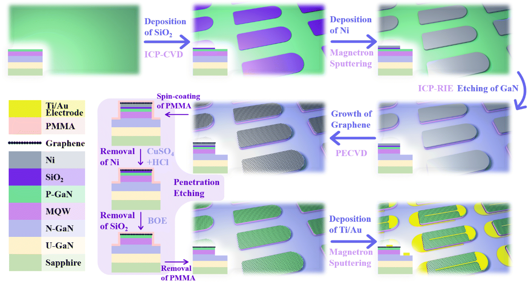 | ||
| Fig. 1 Schematic diagram of the process flow and chip structures of LEDs with transfer-free patterned graphene as transparent electrodes. Three-dimensional diagrams and cross-sectional diagrams are presented for clearer illustration. Abbreviations: ICP, inductively coupled plasma; CVD, chemical vapor deposition; RIE, reactive ion etching; PECVD, plasma enhanced chemical vapor deposition; BOE, buffered oxide etching; MQW, multiple quantum well. | ||
The fabricated devices were characterized by scanning electron microscopy (SEM) and energy dispersive spectrometry (EDS), as shown in Fig. 2 and Table 1. From the results, there are no Si or Ni elements in the sample; thus, it can be determined that SiO2 and Ni have been completely etched away even if they are wrapped in PMMA and graphene, which proves the effectiveness of penetration etching. Fig. 2b and c show the SEM images of graphene on LEDs (inlens mode). It can be seen that the mesa is completely covered with uniform graphene. The chiaroscuro pattern is observed due to slight differences in the number of layers of graphene in different locations. However, there are only slight differences in the Raman spectra of graphene at different locations (Fig. S1, ESI†), which may be due to the fact that small changes in the number of layers do not have a large impact on the Raman spectra of multilayer graphene (see below for a detailed analysis of the Raman spectra of graphene). Fig. 2c shows the edge area of the LED mesa. From left to right, they are the graphene on the mesa, n-GaN, and the N electrode of the LED. It can be seen that graphene is only present on the mesa, which indicates that transfer-free and patterned graphene has been directly obtained. By the circular transmission line model (CTLM) measurements,57,58 the sheet resistance of graphene was measured to be about 1255 Ω sq−1 (Fig. S2 and S3, ESI†), and the contact resistivity between graphene and p-GaN was measured to be about 0.3207 Ω cm2 (Fig. S4 and S5, ESI†). The measurement and calculation details are shown in the ESI.†
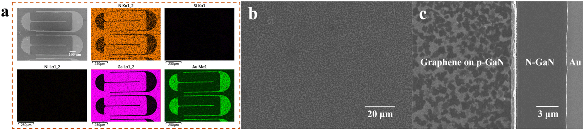 | ||
| Fig. 2 EDS and SEM characterizations of fabricated LEDs. (a) The distribution maps of different elements on the surface of LEDs. (b) SEM image of graphene on the LED mesa (inlens mode). (c) SEM image of the edge of the LED mesa (inlens mode). | ||
| C | N | Ga | Au | Si | Ni | |
|---|---|---|---|---|---|---|
| Weight% | 3.57 | 9.49 | 57.76 | 29.19 | — | — |
| Atom% | 15.22 | 34.72 | 42.46 | 7.6 | — | — |
The SiO2 isolation layer is crucial in this technology. To analyze its effects, graphene transparent electrode LEDs without the SiO2 isolation layer were fabricated for comparison. Fig. 3 shows the Raman characterization of graphene with and without the SiO2 isolation layer on devices at different stages. The characterization of graphene at different experimental stages is done to monitor the condition of graphene in “real time” to determine whether the quality of graphene is affected by penetration etching and the fabrication of metal electrodes. There are three common Raman characteristic peaks of graphene: D peak at 1350 cm−1, G peak at 1580 cm−1, and 2D peak at 2700 cm−1. The D peak is generally associated with the defects of graphene, and the higher its strength, the more defects in graphene. The number of graphene layers is usually estimated in terms of the 2D/G ratio and the shape of the peaks.59 Due to the disordered Raman peaks of GaN at 1000–1500 cm−1, for graphene on the surface of p-GaN, the Raman signal of GaN will be superimposed with that of graphene, resulting in interference; thus, the Raman spectrum of GaN is also shown in Fig. 3 for reference.
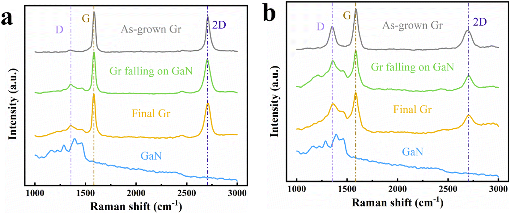 | ||
| Fig. 3 Raman spectra of graphene grown with (a) and without (b) isolation layer at different experimental stages. As-grown Gr: graphene grown on the surface of Ni; Gr falling on GaN: graphene that “falls” on the surface of GaN after penetration etching; final graphene: after the fabrication of electrodes, the final graphene on the LED. | ||
As can be seen from both the figures, there is almost no change in the Raman spectra of graphene before and after the penetration etching and electrode fabrication, indicating that the quality of graphene is hardly affected by these two steps. Compared to graphene with the isolation layer, graphene without the isolation layer has a significant D peak, which is almost half the height of the G peak, indicating that it has more defects. In addition, the intensity ratio of its 2D peak to G peak is much smaller, meaning that it has more layers. Both of them are multi-layer graphene. The graphene with the isolation layer is enough to fully conduct the current, while graphene with even more layers will block the light emitted by the LEDs. It is worth noting that the Raman spectra of graphene with the isolation layer is less affected by the GaN Raman signal. This is because its overall Raman signal intensity is much stronger than that of graphene without the isolation layer, and the Raman signal intensity of GaN in different areas is basically the same, which further proves that the quality of graphene with the isolation layer is better. Clearly, graphene with an SiO2 isolation layer has a great quality advantage, while for the sample without the isolation layer, there may be a reaction between GaN and Ni at high temperatures, which affects the catalytic performance of Ni in graphene growth.
Graphene with and without the isolation layer was characterized by transmission electron microscopy to explore their number of layers, as shown in Fig. 4. Fig. 4a is the high-resolution transmission electron microscopy (HRTEM) image of graphene with the isolation layer, and Fig. 4b is the corresponding selected area electron diffraction (SAED) image. By looking at the edges of graphene in HRTEM and the number of bright spots in SAED, it is speculated that the graphene may be five layers or more. The thickness of graphene was roughly estimated to be 2.7 nm by atomic force microscopy (AFM), as shown in Fig. S6 (ESI†). Fig. 4c is the HRTEM image of graphene without the isolation layer, and Fig. 4d is the corresponding SAED image. The diffraction spots can be seen to converge into rings; thus, it can be inferred that this graphene has more layers. It can be seen that the roughly estimated number of layers of the two graphenes is basically consistent with the results of Raman characterization.
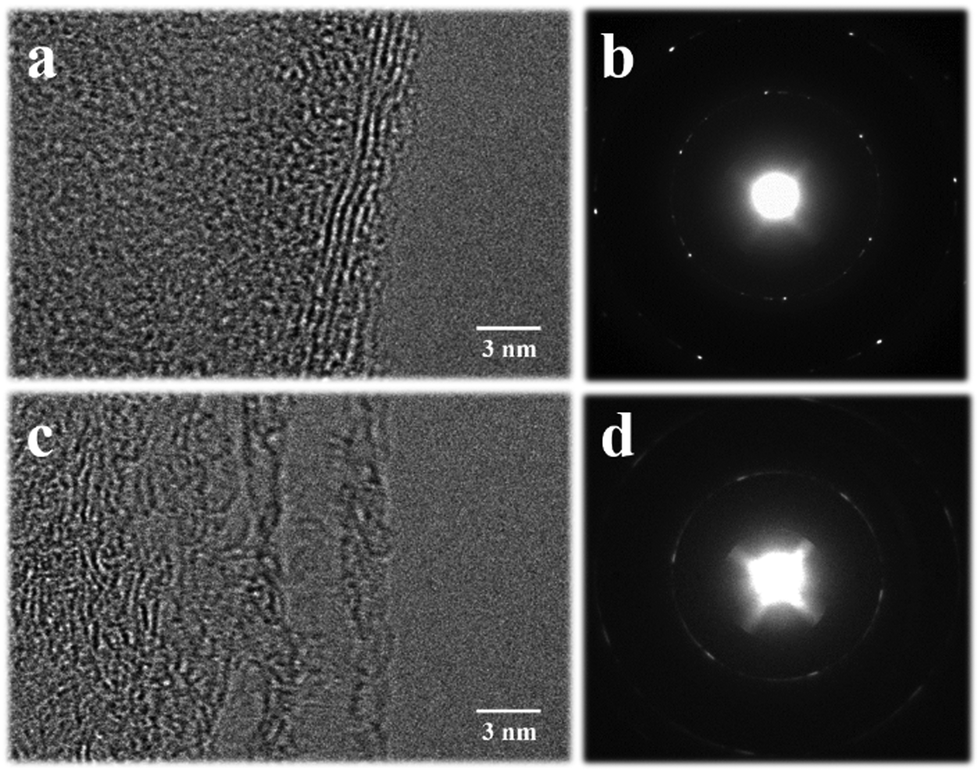 | ||
| Fig. 4 Transmission electron microscopy characterization of graphene with and without isolation layer. (a) and (b) HRTEM image and SAED image of graphene with the isolation layer. (c) and (d) HRTEM image and SAED image of graphene without the isolation layer. | ||
In our experiment, the growth process of graphene is mainly that the gaseous carbon source is pyrolyzed under high temperature and plasma, and then the carbon atoms forms graphene on the sample surface under metal catalysis. In order to further explore the specific effects of high temperature on Ni and GaN during the growth of graphene and the protective effect of SiO2 isolation layer, four samples were prepared on the same GaN epitaxial wafer, as shown in Fig. 5a. The focus here is on the interaction between GaN, Ni and SiO2 at high temperatures rather than graphene. If the sample surface is covered with graphene, it will be detrimental to our characterization of the sample surface. Therefore, the four samples were treated with PECVD under the conditions of growing graphene but without the carbon source, which provides a state that approximates graphene growth while preventing graphene from forming on the sample surface. Then, the Ni and SiO2 of sample 2 and the Ni of sample 4 were etched away. These four samples were characterized by SEM and EDS to observe Ni on samples 1 and 3 and GaN on samples 2 and 4. The penetration depth of EDS was 200 nm.
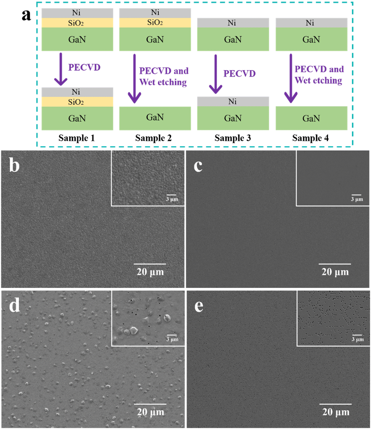 | ||
| Fig. 5 Four samples were prepared to explore the effect of 650 °C temperature on Ni and GaN as well as the isolation effect of SiO2. (a) The structural diagram and processing method of the samples. The thickness of the Ni layer is 250 nm, and the thickness of the SiO2 layer is 100 nm. (b)–(e) SEM images (SE2 mode) of samples 1–4 in sequence. | ||
Table 2 shows the percentage of elemental content in samples 1–4 characterized by EDS for the analysis of Ni and GaN. For samples with the SiO2 isolation layer, the Ni surface is uniformly gravel-like, which is a normal Ni annealed morphology (Fig. 5b). As can be seen from Fig. 5c, the surface of GaN protected by the isolation layer is very flat, and it can be considered that it has not suffered any damage during the entire process. However, for samples without the SiO2 isolation layer, irregular bumps and holes formed on the Ni surface (Fig. 5d), which is likely to introduce more defects on the grown graphene. More importantly, the EDS results indicate that the Ni in sample 3 has been mixed with Ga, which will affect the catalytic performance of Ni and reduce the quality of the grown graphene, consistent with the Raman results. This phenomenon can be attributed to the fact that when GaN and Ni are in direct contact at 650 °C, a portion of Ga atoms gradually diffuses into the Ni layer, resulting in Ga vacancies in GaN.60 After losing some Ga atoms, the N atoms become less stable, escaping from the sample surface in the form of N2 and forming small holes at the grain boundaries of Ni. In addition, as can be seen from Fig. 5e, the loss of N and Ga atoms leads to dense hexagonal holes on the GaN surface, which will greatly affect the performance of LEDs fabricated on this basis. It is worth noting that Al element was detected in the EDS characterization of sample 4 because there is an AlGaN electron blocking layer in addition to p-GaN in the 200 nm-thick surface layer of the GaN epitaxial wafer. The proportion of Al atoms is so low that no Al element is detected in sample 2, but Al is detected in sample 4 because the loss of some N and Ga atoms increases the proportion of Al atoms.
| Elements | Weight% | Atom% | ||||||
|---|---|---|---|---|---|---|---|---|
| SP 1 | SP 2 | SP 3 | SP 4 | SP 1 | SP 2 | SP 3 | SP 4 | |
| Abbreviation: SP, sample. | ||||||||
| C | 3.8 | 2.59 | 2.97 | 2.84 | 16.2 | 8.77 | 13.32 | 9.37 |
| N | — | 14.86 | — | 14.59 | — | 43.11 | — | 41.29 |
| Ni | 96.2 | — | 81.05 | — | 83.8 | — | 74.34 | — |
| Ga | — | 82.55 | 15.98 | 79.94 | — | 48.12 | 12.34 | 45.46 |
| Al | — | — | — | 2.64 | — | — | — | 3.88 |
Three-dimensional AFM images and roughness of the four samples are shown in Fig. 6. The characterization range of GaN (sample 2, 4) was selected as 5 μm × 5 μm, and the characterization range of Ni (sample 1, 3) was selected as 10 μm × 10 μm because Ni has a larger amplitude of morphological change. In order to facilitate the observation of the differences of GaN and Ni on different samples, the vertical scale of samples 1 and 3 is −80 to 110 nm, and the vertical scale of samples 2 and 4 is −20 to 15 nm. It can be seen that the AFM results and SEM results are basically consistent. In addition, the two-dimensional AFM images and the height profiles of the selected sections are shown in Fig. S7 (ESI†) in order to specify the height variation in detail.
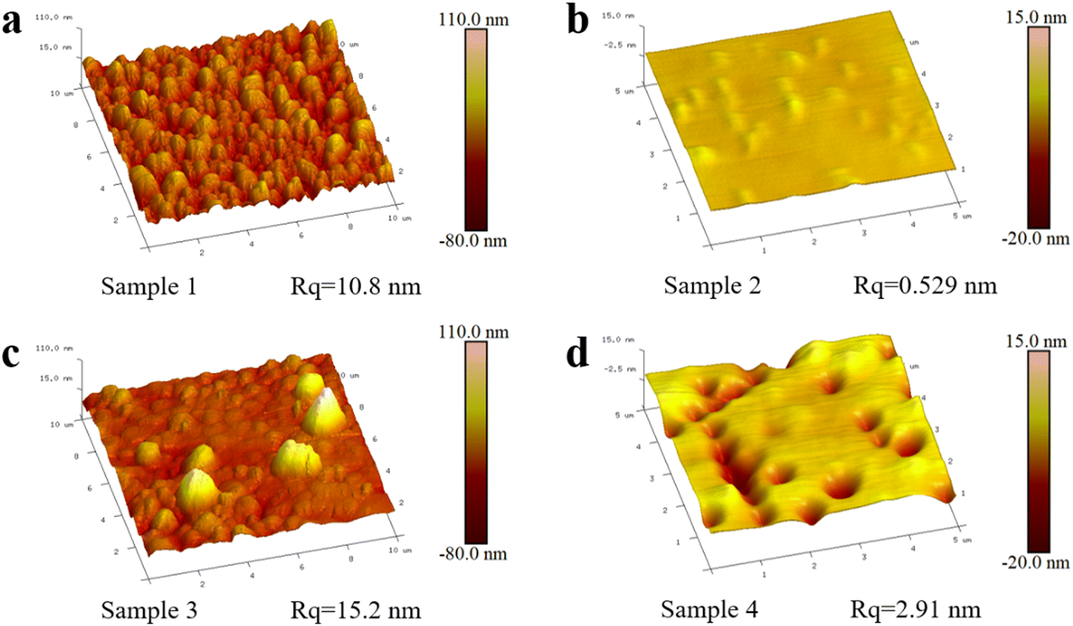 | ||
| Fig. 6 Three-dimensional AFM images and roughness of the four samples. (a) Sample 1. (b) Sample 2. (c) Sample 3. (d) Sample 4. | ||
In short, the SiO2 isolation layer greatly protects the catalytic ability of Ni and the integrity of the GaN substrate, which is the basis for the application of this technology to metal and semiconductor substrates.
In order to visually demonstrate the performance of the graphene transparent electrodes, LEDs with 70 nm-thick ITO transparent electrodes and LEDs without transparent electrodes were also fabricated for comparison. Fig. 7a shows the current–voltage characteristics of the LEDs, and the inset shows the current–voltage characteristics in the semi-log scale to facilitate the observation of the leakage current of LEDs. Fig. 7b shows the optical microscopy images of four LEDs at either 20 mA or 100 mA. The ideal turn-on voltage for the LEDs is approximately 2.8–2.9 V. It can be seen that the LEDs with ITO have almost no leakage current, reaching 100 mA at about 4.8 V, with excellent electrical performance, and the entire mesa emits bright light evenly. The graphene LEDs with an isolation layer also have no leakage current, but they need about 5.6 V to reach 100 mA, which indicates that the series resistance of the graphene LEDs is larger than that of ITO LEDs. Their luminous image is almost indistinguishable from that of LEDs with ITO, achieving a good current spreading. The LEDs without transparent electrodes have a leakage current of about 10 mA, and because there is no transparent electrode to provide current spreading, only the area connected to the metal electrodes can emit light, which leads to their extremely weak light so that only a faint “white light” can be seen in the luminous image, even at 100 mA. The leakage current generated by the graphene LEDs without the isolation layer is the largest of the four LEDs, and the discontinuous and uneven light emitting can be seen from the luminous image. According to the previous analysis, one reason for this phenomenon is the low quality of this graphene, and the more important reason may be that the p-GaN surface was damaged during graphene growth, which weakens the performance of the LEDs.
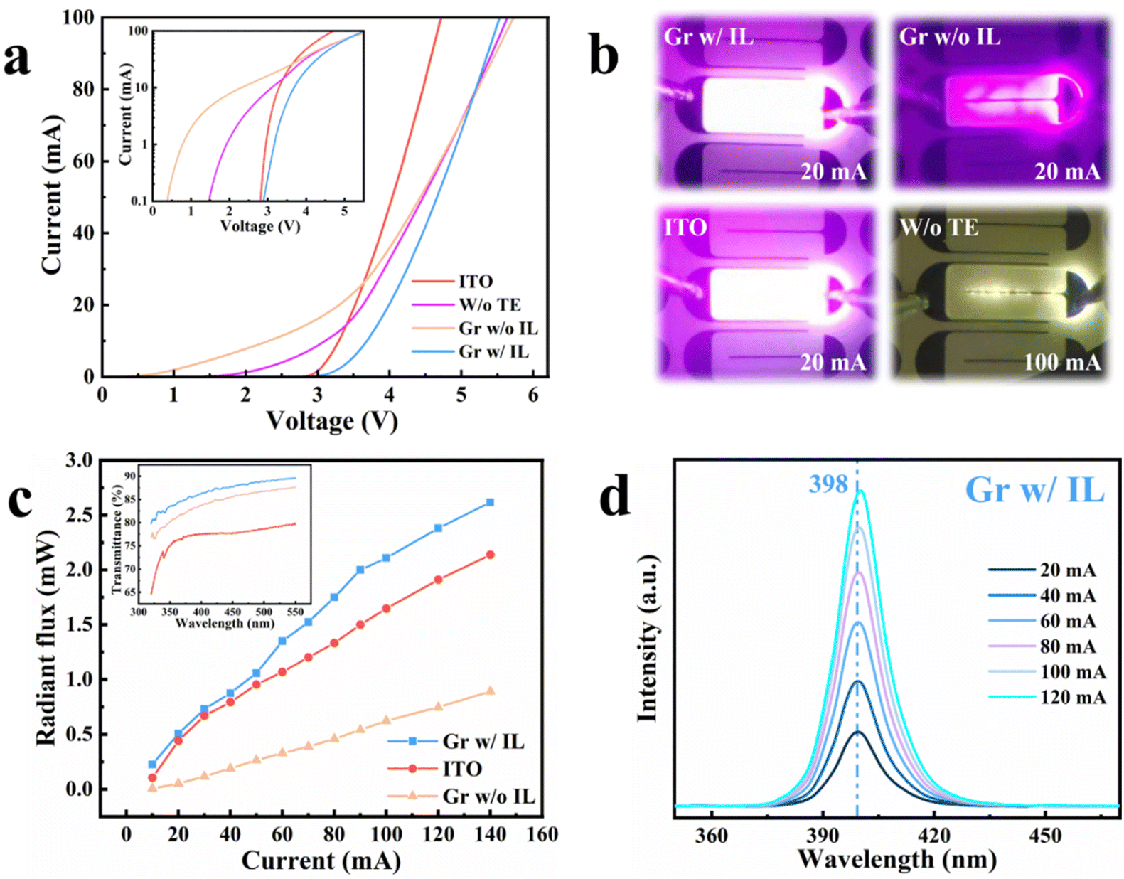 | ||
| Fig. 7 Electrical and optical properties of LEDs fabricated by different methods, including LEDs with ITO transparent electrodes (shown as ITO, the same below), LEDs without transparent electrodes (W/o TE), graphene LEDs without the isolation layer (Gr w/o IL) and graphene LEDs with the isolation layer (Gr w/IL). (a) Current–voltage characteristics of LEDs. The inset is the current–voltage characteristics in the semi-log scale. (b) Optical microscope images of LEDs at 20 mA or 100 mA. (c) The radiant flux of LEDs as a function of current. The inset shows the transmittance of ITO, graphene with the isolation layer and graphene without the isolation layer. (d) Electroluminescence spectra of the graphene LEDs with isolation layer (Gr w/IL) at different currents. | ||
Since the LEDs without transparent electrodes emit too little light to be measured optically, Fig. 7c shows the radiant flux of three LEDs as a function of current. The inset shows the transmittance of ITO, graphene without the isolation layer and graphene with the isolation layer from 320 nm to 550 nm. Consistent with the luminous image, the radiant flux of the graphene LEDs without the isolation layer is very low. Surprisingly, the radiant flux of the graphene LEDs with the isolation layer is higher than that of the ITO LEDs, even though their current–voltage characteristic is not as good, which should be attributed to one of the advantages of graphene—higher transmittance. The transmittance of ITO decreases sharply in the ultraviolet band as the wavelength decreases, which means that graphene will show greater competitiveness in ultraviolet LEDs. In addition, graphene without the isolation layer has a lower transmittance than graphene with the isolation layer, meaning that it has more layers, which is consistent with the Raman results. Because the three LEDs are from the same wafer, their electroluminescence spectra are not very different at the normalized intensity coordinates; thus, only the electroluminescence spectra of the graphene LEDs with the isolation layer are shown here (Fig. 7d). It can be seen that as the current increases, the temperature of the device increases, resulting in a redshift in the luminous wavelength.
Table 3 is a comparison of several graphene preparation studies in terms of technical characteristics, process conditions, and graphene properties. It can be seen that our technology has certain advantages in terms of transfer-free patterning, suitable for semiconductors and short growth time, but there is still room for improvement in the sheet resistance of graphene. In addition, it has recently been reported that reasonable quality graphene has been prepared at rather low temperatures and devices with acceptable performance have been prepared with it,61–63 which may be one of our future research directions for further refinement.
| Equipment | Transfer-free or not | Patterning or not | Temperature (°C) | Time (min) | Metal catalysts | Target substrates | Number of layers | Sheet resistance (KΩ □−1) | Transmittance@398 nm | Ref. |
|---|---|---|---|---|---|---|---|---|---|---|
| Abbreviation: PATCVD, plasma-assisted thermal CVD; M–Cu, monocrystalline Cu; P–Cu, polycrystalline Cu. | ||||||||||
| PATCVD | Yes | No | 150 | 90 | Ti | Polyester sulfone | 1 | 0.082 | More than 81% | 63 |
| CVD | Yes | Yes | 935 | 20 | Mo | Parylene | 7 | 0.565 | ∼77% | 24 |
| 40 | 10 | 0.461 | ∼71% | |||||||
| 60 | 17 | 0.23 | ∼59% | |||||||
| CVD | Yes | No | 300 | 40 | M–Cu | SiO2 | 1 | 0.093–0.121 | ∼96.2 | 61 |
| CVD | No | No | 1005 | 20 | M–Cu | — | 1 | 0.314 | ∼96% | 37 |
| P–Cu | 1 | 0.362 | ∼95.4% | |||||||
| PECVD | Yes | No | 600 | 2 | — | Glass | ∼10 | 1.6 | ∼77% | 45 |
| ∼14 | 1.4 | ∼66% | ||||||||
| ∼16 | 0.97 | ∼61% | ||||||||
| PECVD | Yes | Yes | 650 | 5 | Ni | GaN | 5 or more | 1.25 | ∼86% | This work |
3. Conclusions
In this paper, a technology for the fabrication of transfer-free, patterned graphene on dielectric, semiconductor or weakly catalytic metal substrate is presented, and the graphene transparent electrodes on GaN-based LED with 398 nm wavelength is fabricated accordingly. The core of this technology is mainly three: the penetration etching process, the Ni masking and catalytic layer and the SiO2 isolation layer. Among them, penetration etching is the foundation of this technology. Ni was selected as both the etching mask and graphene growth catalyst because of its high hardness and good catalytic properties. It performs an excellent auxiliary role and simplifies the process. SiO2 is used to isolate the Ni layer and the substrate, allowing the technology to be applied to a wider variety of substrates and serve more fields. The results show that high-quality, transfer-free, patterned graphene has been fabricated, which as transparent electrodes achieve good current expansion and light transmission, and their performance is even slightly better than that of ITO. In addition, the growth of graphene in PECVD can be continuously optimized in the future to obtain even higher quality graphene. The process of this technology is simple but the effect is remarkable, which provides a new solution for the scalable application of graphene.4. Experimental details
The epitaxial wafer used was provided by Xiangneng Hualei Optoelectronics Company, which can withstand a maximum temperature of 700 °C. If the temperature is higher than this, the GaN may decompose partially because in the graphene CVD we do not have a proper protection atmosphere, which a standard GaN metal–organic CVD uses. On the other hand, usually the higher the growth temperature, the better the quality of graphene. Thus, in this paper, 650 °C was selected as the growth temperature due to the consideration of graphene quality and experimental stability.Graphene LEDs with and without isolation layer
First, a 100 nm SiO2 film and a 250 nm Ni film were deposited on the sample (for the graphene LEDs without the isolation layer, only a 250 nm Ni film was deposited) and patterned in a single lithography. With Ni as the mask, the LED mesas of 300 × 700 μm2 were obtained by ICP-RIE. Subsequently the sample was treated in PECVD at 650 °C and 6 mbar under an atmosphere of CH4/H2/Ar (5/20/960 sccm) at a plasma power of 40 W for 5 min. After the growth of graphene, PMMA was spin-coated (3000 rpm for 30 s) on the sample and baked at 150 °C for 12 min. The sample was then immersed in the etching solution (CuSO4![[thin space (1/6-em)]](https://www.rsc.org/images/entities/char_2009.gif) :HCl:H2O = 10 g:50 mL:50 mL) for more than four hours to etch the Ni layer away. For graphene LEDs with the isolation layer, the sample was then immersed in BOE (HF:NH3F:H2O = 3 mL:6 g:60 mL) for more than four hours to etch away the SiO2 isolation layer. After natural drying, the sample was baked at 150 °C for 10 minutes to strengthen the contact between graphene and GaN. Then, PMMA was removed by acetone and isopropyl alcohol. Finally, 15 nm Ti and 80 nm Au were lithographically sputtered as the metal electrodes.
:HCl:H2O = 10 g:50 mL:50 mL) for more than four hours to etch the Ni layer away. For graphene LEDs with the isolation layer, the sample was then immersed in BOE (HF:NH3F:H2O = 3 mL:6 g:60 mL) for more than four hours to etch away the SiO2 isolation layer. After natural drying, the sample was baked at 150 °C for 10 minutes to strengthen the contact between graphene and GaN. Then, PMMA was removed by acetone and isopropyl alcohol. Finally, 15 nm Ti and 80 nm Au were lithographically sputtered as the metal electrodes.
ITO LEDs and LEDs without transparent electrodes
There is only one difference in the fabrication of these two LEDs, i.e., for ITO LEDs, the ITO of 110 nm is pre-deposited on the epitaxial wafer surface by reactive plasma deposition. First, an Ni mask of 250 nm was deposited on the sample surface and patterned by lithography. The 300 × 700 μm2 mesas were then obtained by ICP-RIE (in the case of ITO LEDs, ITO outside the mesa was also etched away in this process). Finally, 15 nm Ti and 80 nm Au were lithographically sputtered.Author contributions
Penghao Tang: conceptualization, data curation, methodology and writing – original draft. Jie Sun: conceptualization, funding acquisition, supervision and writing – review & editing. Yu Mei: investigation and methodology. Zaifa Du, Aoqi Fang, Fangzhu Xiong: investigation and data curation. Weiling Guo: funding acquisition, resources and supervision.Conflicts of interest
There are no conflicts to declare.Acknowledgements
We thank the support from National Key Research and Development Program of China (No. 2023YFB3608700 and 2023YFB3608703), Fujian Science & Technology Innovation Laboratory for Optoelectronic Information of China (No. 2021ZZ122 and 2020ZZ110), and Fujian provincial projects (No. 2021HZ0114 and 2021J01583).Notes and references
- K. S. Novoselov, A. K. Geim, S. V. Morozov, D. Jiang, Y. Zhang, S. V. Dubonos, I. V. Grigorieva and A. A. Firsov, Science, 2004, 306, 666, DOI:10.1126/science.1102896.
- R. R. Nair, P. Blake, A. N. Grigorenko, K. S. Novoselov, T. J. Booth, T. Stauber, N. M. R. Peres and A. K. Geim, Science, 2008, 320, 1308, DOI:10.1126/science.1156965.
- K. I. Bolotina, K. J. Sikes, Z. Jiang, M. Klima, G. Fudenberg, J. Hone, P. Kim and H. L. Stormer, Solid State Commun., 2008, 146, 351, DOI:10.1016/j.ssc.2008.02.024.
- L. A. Falkovsky, J. Phys.: Conf. Ser., 2008, 129, 012004, DOI:10.1088/1742-6596/129/1/012004.
- C. Lee, X. Wei, J. W. Kysar and J. Hone, Science, 2008, 321, 385, DOI:10.1126/science.1157996.
- N. Gao and X. Fang, Chem. Rev., 2015, 115, 8294, DOI:10.1021/cr400607y.
- S. Nakamura, T. Mukai, M. S. M. Senoh and N. I. N. Iwasa, Jpn. J. Appl. Phys., 1992, 31, L139, DOI:10.1143/JJAP.31.L139.
- H. Amano, M. Kito, K. Hiramatsu and I. Akasaki, Jpn. J. Appl. Phys., 1989, 28, L2112, DOI:10.1143/JJAP.28.L2112.
- Q. Li, Y. Li, M. Zhang, W. Ding and F. Yun, Chin. Phys. B, 2016, 25, 117102, DOI:10.1088/1674-1056/25/11/117102.
- D. Y. Kang, B.-H. Kim, T. H. Lee, J. W. Shim, S. Kim, H.-J. Sung, K. J. Chang and T. G. Kim, Nano-Micro Lett., 2021, 13, 211, DOI:10.1007/s40820-021-00735-y.
- X. Fan, S. Xu, Y. Huang, W. Liu, H. Tao, J. Zhang and Y. Hao, ECS J. Solid State Sci. Technol., 2023, 12, 096001, DOI:10.1149/2162-8777/acf39d.
- B.-J. Kim, C. Lee, Y. Jung, K. H. Baik, M. A. Mastro, J. K. Hite, C. R. Eddy, Jr. and J. Kim, Appl. Phys. Lett., 2011, 99, 143101, DOI:10.1063/1.3644496.
- G. Jiang, H. Tian, X.-F. Wang, T. Hirtz, F. Wu, Y.-C. Qiao, G.-Y. Gou, Y.-H. Wei, J.-M. Yang, S. Yang, Y. Yang and T.-L. Ren, Nanoscale Adv., 2019, 1, 4745, 10.1039/c9na00550a.
- F. Li, Z. Lin, B. Zhang, Y. Zhang, C. Wu and T. Guo, Org. Electron., 2013, 14, 2139, DOI:10.1016/j.orgel.2013.05.023.
- J. Miao and T. Fan, Carbon, 2023, 202, 495, DOI:10.1016/j.carbon.2022.11.018.
- M.-S. Chae, T. H. Lee, K. R. Son, Y. W. Kim, K. S. Hwang and T. G. Kim, Nanoscale Horiz., 2019, 4, 610, 10.1039/c8nh00374b.
- J. H. Kang, S. Choi, Y. J. Park, J. S. Park, N. S. Cho, S. Cho, B. Walker, D. S. Choi, J.-W. Shin and J. H. Seo, Carbon, 2021, 171, 341, DOI:10.1016/j.carbon.2020.08.055.
- I.-J. Park, T. I. Kim and S.-Y. Choi, ACS Appl. Mater. Interfaces, 2022, 14, 43907, DOI:10.1021/acsami.2c12006.
- L.-P. Ma, Z. Wu, Y. Yan, D. Zhang, S. Dong, J. Du, D. Ma, H.-M. Cheng and W. Ren, Nano Res., 2023, 16, 12788, DOI:10.1007/s12274-023-6176-y.
- L. Wang, W. Liu, Y. Zhang, Z.-H. Zhang, S. T. Tan, X. Yi, G. Wang, X. Sun, H. Zhu and H. V. Demir, Nano Energy, 2015, 12, 419, DOI:10.1016/j.nanoen.2014.12.035.
- S. Chandramohan, J. H. Kang, Y. S. Katharria, N. Han, Y. S. Beak, K. B. Ko, J. B. Park, B. D. Ryu, H. K. Kim, E.-K. Suh and C.-H. Hong, J. Phys. D: Appl. Phys., 2012, 45, 145101, DOI:10.1088/0022-3727/45/14/145101.
- J.-P. Shim, T. H. Seo, J.-H. Min, C. M. Kang, E.-K. Suh and D.-S. Lee, Appl. Phys. Lett., 2013, 102, 151115, DOI:10.1063/1.4802800.
- H. Zhong, Z. Liu, L. Shi, G. Xu, Y. Fan, Z. Huang, J. Wang, G. Ren and K. Xu, Appl. Phys. Lett., 2014, 104, 212101, DOI:10.1063/1.4880732.
- N. B. Babaroud, M. Palmar, A. I. Velea, C. Coletti, S. Weingärtner, F. Vos, W. A. Serdijn, S. Vollebregt and V. Giagka, Microsyst. Nanoeng., 2022, 8, 107, DOI:10.1038/s41378-022-00430-x.
- A. E. Adetayo, T. N. Ahmed, A. Zakhidov and G. W. Beall, Adv. Optical Mater., 2021, 9, 2002102, DOI:10.1002/adom.202002102.
- G. W. Cushing, V. Johanek, J. K. Navin and I. Harrison, J. Phys. Chem. C, 2015, 119, 4759, DOI:10.1021/jp508177k.
- D. Eom, D. Prezzi, K. T. Rim, H. Zhou, M. Lefenfeld, S. Xiao, C. Nuckolls, M. S. Hybertsen, T. F. Heinz and G. W. Flynn, Nano Lett., 2009, 9, 2844, DOI:10.1021/nl900927f.
- S. Pekdemir, M. S. Onses and M. Hancer, Surf. Coat. Technol., 2017, 309, 814, DOI:10.1016/j.surfcoat.2016.10.081.
- Z. Li, P. Wu, C. Wang, X. Fan, W. Zhang, X. Zhai, C. Zeng, Z. Li, J. Yang and J. Hou, ACS Nano, 2011, 5, 3385, DOI:10.1021/nn200854p.
- Z. Sun, Z. Yan, J. Yao, E. Beitler, Y. Zhu and J. M. Tour, Nature, 2010, 468, 549, DOI:10.1038/nature09579.
- J. Pang, A. Bachmatiuk, I. Ibrahim, L. Fu, D. Placha, G. S. Martynkova, B. Trzebicka, T. Gemming, J. Eckert and M. H. Rümmeli, J. Mater. Sci., 2016, 51, 640, DOI:10.1007/s10853-015-9440-z.
- X. Li, W. Cai, L. Colombo and R. S. Ruoff, Nano Lett., 2009, 9, 4268, DOI:10.1021/nl902515k.
- S. Chandramohan, K. B. Ko, J. H. Yang, B. D. Ryu, Y. S. Katharria, T. Y. Kim, B. J. Cho and C.-H. Hong, J. Appl. Phys., 2014, 115, 054503, DOI:10.1063/1.4863640.
- K. S. Kim, Y. Zhao, H. Jang, S. Y. Lee, J. M. Kim, K. S. Kim, J.-H. Ahn, P. Kim, J.-Y. Choi and B. H. Hong, Nature, 2009, 457, 706, DOI:10.1038/nature07719.
- S. Chandramohan, J. H. Kang, Y. S. Katharria, N. Han, Y. S. Beak, K. B. Ko, J. B. Park, H. K. Kim, E.-K. Suh and C.-H. Hong, Appl. Phys. Lett., 2012, 100, 023502, DOI:10.1063/1.3675631.
- J.-H. Min, M. Son, S.-Y. Bae, J.-Y. Lee, J. Yun, M.-J. Maeng, D.-G. Kwon, Y. Park, J.-I. Shim, M.-H. Ham and D.-S. Lee, Opt. Express, 2014, 22, A1040, DOI:10.1364/OE.22.0A1040.
- J. S. Roh, J. K. Jang, N. Kwon, S. Bok, Y. J. Kim, C. Jeon, H. W. Yoon, H. W. Kim, B. Lim and H. B. Park, Carbon, 2021, 178, 181, DOI:10.1016/j.carbon.2021.02.097.
- Q. Liu, Y. Gong, T. Wang, W.-L. Chan and J. Wu, Carbon, 2016, 96, 203, DOI:10.1016/j.carbon.2015.09.075.
- S. C. Xu, B. Y. Man, S. Z. Jiang, C. S. Chen, C. Yang, M. Liu, X. G. Gao, Z. C. Sun and C. Zhang, CrystEngComm, 2013, 15, 1840, 10.1039/c3ce27029g.
- M.-Y. Lin, C.-F. Su, S.-C. Lee and S.-Y. Lin, J. Appl. Phys., 2014, 115, 223510, DOI:10.1063/1.4883359.
- J. Chen, Y. Wen, Y. Guo, B. Wu, L. Huang, Y. Xue, D. Geng, D. Wang, G. Yu and Y. Liu, J. Am. Chem. Soc., 2011, 133, 17548, DOI:10.1021/ja2063633.
- A. Khan, S. M. Islam, S. Ahmed, R. R. Kumar, M. R. Habib, K. Huang, M. Hu, X. Yu and D. Yang, Adv. Sci., 2018, 5, 1800050, DOI:10.1002/advs.201800050.
- R. Muñoz, C. Munuera, J. I. Martínez, J. Azpeitia, C. Gómez-Aleixandre and M. García-Hernández, 2D Mater., 2017, 4, 015009, DOI:10.1088/2053-1583/4/1/015009.
- J. Chen, Y. Guo, Y. Wen, L. Huang, Y. Xue, D. Geng, B. Wu, B. Luo, G. Yu and Y. Liu, Adv. Mater., 2013, 25, 992, DOI:10.1002/adma.201202973.
- M. S. A. Kamel, C. T. Stoppiello and M. V. Jacob, Carbon, 2023, 202, 150, DOI:10.1016/j.carbon.2022.11.017.
- Z. Peng, Z. Yan, Z. Sun and J. M. Tour, ACS Nano, 2011, 5, 8241, DOI:10.1021/nn202923y.
- D. Wang, H. Tian, Y. Yang, D. Xie, T.-L. Ren and Y. Zhang, Sci. Rep., 2013, 3, 1348, DOI:10.1038/srep01348.
- I. Martin-Fernandez, D. Wang and Y. Zhang, Nano Lett., 2012, 12, 6175, DOI:10.1021/nl302993m.
- R. Hirano, K. Matsubara, G. Kalita, Y. Hayashia and M. Tanemura, Nanoscale, 2012, 4, 7791, 10.1039/c2nr31723k.
- T. Kato and R. Hatakeyama, ACS Nano, 2012, 6, 8508, DOI:10.1021/nn302290z.
- Z. Yan, Z. Peng, Z. Sun, J. Yao, Y. Zhu, Z. Liu, P. M. Ajayan and J. M. Tour, ACS Nano, 2011, 5, 8187, DOI:10.1021/nn202829y.
- C. Y. Chen, D. Dai, G. X. Chen, J. H. Yu, K. Nishimura, C.-T. Lin, N. Jiang and Z. L. Zhan, Appl. Surf. Sci., 2015, 346, 41, DOI:10.1016/j.apsusc.2015.03.204.
- Y. Dong, Y. Xie, C. Xu, X. Li, J. Deng, X. Fan, G. Pan, Q. Wang, F. Xiong, Y. Fu and J. Sun, APL Mater., 2018, 6, 026802, DOI:10.1063/1.4992077.
- Y. Dong, Y. Xie, C. Xu, Y. Fu, X. Fan, X. Li, L. Wang, F. Xiong, W. Guo, G. Pan, Q. Wang, F. Qian and J. Sun, Nanotechnology, 2018, 29, 365301, DOI:10.1063/1.4992077.
- Y. Dong, S. Guo, H. Mao, C. Xu, Y. Xie, C. Cheng, X. Mao, J. Deng, G. Pan and J. Sun, Nanomaterials, 2019, 9, 1633, DOI:10.3390/nano9111633.
- Y. Dong, S. Guo, H. Mao, C. Xu, Y. Xie, J. Deng, L. Wang, Z. Du, F. Xiong and J. Sun, ACS Appl. Electron. Mater., 2020, 2, 238, DOI:10.1021/acsaelm.9b00719.
- G. S. Marlow and M. B. Das, Solid-State Electron., 1982, 25, 91, DOI:10.1016/0038-1101(82)90036-3.
- L. Wang, Y. Zhang, X. Li, Z. Liu, E. Guo, X. Yi, J. Wang, H. Zhu and G. Wang, J. Phys. D: Appl. Phys., 2012, 45, 505102, DOI:10.1088/0022-3727/45/50/505102.
- A. C. Ferrari, J. C. Meyer, V. Scardaci, C. Casiraghi, M. Lazzeri, F. Mauri, S. Piscanec, D. Jiang, K. S. Novoselov, S. Roth and A. K. Geim, Phys. Rev. Lett., 2006, 97, 187401, DOI:10.1103/PhysRevLett.97.187401.
- I. Chary, A. Chandolu, B. Borisov, V. Kuryatkov, S. Nikishin and M. Holtz, J. Electron. Mater., 2009, 38, 545, DOI:10.1007/s11664-008-0655-5.
- F. Qian, J. Deng, Y. Dong, C. Xu, L. Hu, G. Fu, P. Chang, Y. Xie and J. Sun, ACS Appl. Mater. Interfaces, 2022, 14, 53174, DOI:10.1021/acsami.2c16505.
- T. Kang, A. Rani, W. Ren, M. J. Sultan, N.-E. Lee and T. G. Kim, J. Mater. Sci. Technol., 2024, 183, 215, DOI:10.1016/j.jmst.2023.10.029.
- V.-D. Tran, S. V. N. Pammi, B.-J. Park, Y. Han, C. Jeon and S.-G. Yoon, Nano Energy, 2019, 65, 104018, DOI:10.1016/j.nanoen.2019.104018.
Footnote |
| † Electronic supplementary information (ESI) available. See DOI: https://doi.org/10.1039/d3tc04656g |
| This journal is © The Royal Society of Chemistry 2024 |