
 Open Access Article
 This Open Access Article is licensed under a Creative Commons Attribution-Non Commercial 3.0 Unported Licence
Heterometallic {Re4Mo2Qi8} cluster-based building blocks: towards the rational nanoarchitectonics of optimized photoelectrodes for solar cells and water splitting†
Tatiana I.
Lappi
ab,
Stéphane
Cordier
*a,
Yakov M.
Gayfulin
 b,
Soraya
Ababou-Girard
c,
Ngan T. K.
Nguyen
de,
Fabien
Grasset
ad,
Tetsuo
Uchikoshi
df,
Nikolay G.
Naumov
b and
Adèle
Renaud
*a
b,
Soraya
Ababou-Girard
c,
Ngan T. K.
Nguyen
de,
Fabien
Grasset
ad,
Tetsuo
Uchikoshi
df,
Nikolay G.
Naumov
b and
Adèle
Renaud
*a
aUniv Rennes, CNRS, ISCR-UMR, 6226, F-35000 Rennes, France. E-mail: Stephane.cordier@univ-rennes.fr; adele.renaud@univ-rennes.fr
bNikolaev Institute of Inorganic Chemistry, Siberian Branch of Russian Academy of Sciences, 3 Acad. Lavrentiev pr., 630090 Novosibirsk, Russia
cUniv Rennes, CNRS, IPR (Institut de Physique de Rennes) – UMR 6251, F-35000, Rennes, France
dCNRS-Saint-Gobain-NIMS, IRL 3629, Laboratory for Innovative Key Materials and Structures (LINK), National Institute for Materials Science, 305-0044 Tsukuba, Japan
eInternational Center for Young Scientists, Global Networking Division, National Institute for Materials Science, 1-2-1 Sengen, Tsukuba, Ibaraki 305-0047, Japan
fResearch Center for Electronic and Optical Materials, National Institute for Materials Science, 1-2-1 Sengen, Tsukuba, Ibaraki 305-0047, Japan
First published on 18th April 2024
Abstract
Metal atom clusters are well-defined nanoscale objects containing a precise number of metal atoms and ligands. Face-capped cluster units of the type [{M6Li8}L′a6] (M = Mo, Re, L = S, Se or I, L′ = Cl, Br, I, CN or H2O) exhibit unique optical and electronic properties that make them relevant building blocks for the rational design of nanomaterials using nanoarchitectonic concepts. Photoelectrodes based on Mo6 and Re6 clusters with various compositions obtained by deposition of uniform layers of those building blocks onto semiconducting surfaces were recently reported. Remarkably, high quality interfaces were formed not only between building blocks but also between the building blocks and the semiconducting surfaces. On the one hand, layers based on active {Mo6Ii8} cluster cores exhibit an ambipolar behavior like carbon nanotube, graphene and transition metal chalcogenides. On the other hand, mixing the two types of {Re6Si8} and {Re6Sei8}-based building blocks enables the creation of micro-(p–n) junctions with enhanced photogenerated current intensity. Herein, we report new advances in the design of photoelectrodes using heterometallic Re4Mo2 cluster-based building blocks. The association of Mo and Re in {Re4Mo2Qi8} cluster cores (Q = S and Se) leads to electronic properties and absorption properties significantly different from those of homometallic {Mo6Ii8} and {Re6Qi8}. Indeed, beyond different molecular orbital diagrams, the {Re4Mo2Qi8} cluster-based units exhibit 22 valence electrons per cluster (VEC) whereas the VEC value for {Mo6Ii8} and {Re6Qi8} cluster units is 24. The mixing of rhenium and molybdenum within the same heterometallic cluster enables not only the optical and transport properties of the active layers to be optimized but it also enables the position of the energy levels to be tuned. This appears very appealing for band alignment engineering in order to design optimized photoelectrodes for solar energy conversion. We show herein that the energy levels of the photoelectrodes built on {Re4Mo2Q8} cluster-based layers immobilized on FTO surfaces are compatible with the photoelectrochemical water splitting.
1. Introduction
Transition metal atom clusters are well-defined nanoscale objects containing a very precise low number of metal atoms and ligands.1 Soluble metal-atom cluster-based compounds with the general formula Ax[{M6Li8}L′a6] (A = alkali, M = Mo, Re; L = I, S, Se; L′ = Cl, I, CN) are prepared by solid-state chemistry. Their syntheses and the solubilization processes are fully detailed in the literature.2–7 In recent years, the nanoarchitectonic concept was applied to the design of photoelectrodes built up from [{M6Li8}L′a6] face-capped octahedral cluster nanobuilding blocks (M = Mo, Re; L = I, S, Se; L′ = Cl, I).3,5,6 According to Ariga,8 “the concept of nanoarchitectonics is supposed to involve the architecting of functional materials using nanoscale units based on the principles of nanotechnology”. Face-capped [{M6Li8}L′a6] (M = Mo, Re, L = S, Se or I, L′ = Cl, Br, I, CN or H2O) building blocks exhibit several singularities compared to other nanosized objects: (i) they are based on an atom-precise composition, (ii) they do not contain toxic metallic elements as it is the case in the well-known CdQ or PbQ QDs (Q = S or Se), (iii) they are not submitted to surface defects (i.e. loss of metal atoms or ligands contrary to semiconducting oxide nanoparticles for which a passivation phenomenon in air results in a reconstructed oxygen-terminated surface for instance9) that could alter their properties, (iv) their properties can be efficiently tuned by chemical engineering by the judicious choice of the metal, capping ligands and terminal ligands, (v) the high solubilization of cluster-based solid-state precursors and the immobilization process onto semiconducting surfaces do not significantly modify the chemical formula of the building blocks that bears comparable properties to those found in bulk compounds. Those singularities constitute significant fundamental differences with nanoparticles of semiconducting sulfides, selenides or oxides.10,11 Indeed, for the latter, a very fine control of the synthesis pathways to control the size of the nanoparticles is mandatory to obtain reproducible chemical and physical properties of nanoparticles with a minimum of surface defects.11 Because such problems are not faced with [{M6Li8}L′a6], they appear as suitable building blocks to design photoelectrodes with high quality interfaces, not only between building blocks but also between the building blocks and the semiconducting surfaces.The properties of bulk compounds and those of layers once immobilized onto surfaces strongly depend on the chemical composition of the [{M6Li8}L′a6] building blocks. For instance, on the one hand, molybdenum cluster iodides based on the {Mo6Ii8} cluster core belong to the family of ambipolar materials like carbon nanotube, graphene and transition metal chalcogenides.6 In ambipolar materials, once hole/electron pairs are created, the holes and electrons are transported simultaneously in opposite directions with comparable kinetics.12,13 Their lifetimes exhibit similar values. Thus, the charge transport is not limited by a minority charge carrier type as it is the case in unipolar semiconductors. The charge transport in p- or n-type semiconductors is restrained by electrons and holes, respectively. Moreover, the molecular electronic structure of the cluster's building blocks is not significantly disturbed by solid-state stacking effects or once deposited on surfaces. Electronic structures of molecular cluster-based compounds and layers are thus related to that of intrinsic inorganic semiconductors. On the other hand, the nature of Q (S or Se) drives the photoelectrochemical properties of photoelectrodes based on {Re6Qi8} cluster-cores.3 The {Re6Si8} sulfide-based photoelectrodes exhibit an ambipolar behaviour with a slight domination of electron on the charge transport, whereas the charge transport in {Re6Sei8} selenide-based photoelectrodes is clearly dominated by the hole transport. Last but not least, photoelectrodes exhibiting tuned electronic properties were obtained by designing active cluster-based layers wherein the ratio between the two {Re6Si8} and {Re6Sei8}-based building blocks was finely controlled. The electric field created by the micro-(p–n) junctions formed by the interactions between the {Re6Si8}- and {Re6Sei8}-based clusters was assumed to limit the recombination of charge carriers and consequently this leads to improvement in the photocurrent generated by such photoelectrodes. A ratio of 1![[thin space (1/6-em)]](https://www.rsc.org/images/entities/char_2009.gif) :1 for {Re6Si8}:{Re6Sei8} maximizes the number of local heterojunctions within the layers and allows optimization of the photophysical properties.3
:1 for {Re6Si8}:{Re6Sei8} maximizes the number of local heterojunctions within the layers and allows optimization of the photophysical properties.3
Herein, we report new advances in the design of photoelectrodes based on octahedral M6 clusters. Following the investigations on Mo6 cluster iodides and Re6 cluster chalcogenides, we explored the photoconductive properties of heterometallic cluster building blocks based on the well-defined {Re4Mo2Qi8} cluster core (Q = S or Se). The mixing of Mo and Re enables us to obtain {Re4Mo2Qi8} cluster-core based building blocks with electronic properties and absorption properties different from those of the homometallic {Mo6Ii8} and {Re6Qi8} (S and Se). Indeed, beyond different molecular orbital diagrams, the cluster units based on {Re4Mo2Qi8} exhibit 22 valence electrons per cluster whereas those based on {Mo6Ii8} and {Re6Qi8} (S and Se) exhibit 24 valence electrons per cluster. After solid-state syntheses and excision in solution of the cluster building blocks, they were precipitated with tetrabutylammonium cations to form the ((C4H9)4N)4[{Re4Mo2Si8}(CN)a6] and ((C4H9)4N)4[{Re4Mo2Sei8}(CN)a6] starting precursors. After solubilization of the latter in acetonitrile, the cluster building blocks were deposited onto FTO surfaces using an electrophoretic deposition (EPD) process.3,5–7,14 The energy diagrams of the photoelectrodes made of {Re4Mo2Qi8} cluster-core based building blocks deposited on FTO are different and lead to different physical and photochemical properties than those made of homometallic {Mo6Ii8} and {Re6Qi8}-based clusters (S and Se) deposited onto surfaces. It was shown that after deposition, the active layers exhibit the following formula: (Bu4N)2(H3O)2[{Re4Mo2Qi8}(CN)a6]·xH2O (Q = S, Se)-based films (Bu4N = (n-C4H9)4N). Their physical properties were then investigated through (photo)electrochemical characterizations. An ambipolar behavior was evidenced for both S and Se chalcogenides. However, in accordance with the previous results obtained on Re6-based films,3 the charge transfer is dominated by electrons in the sulfide layer and, reversely, by holes in the selenide one. Moreover, thanks to the mixing of Re and Mo, the positions of energy levels of {Re4Mo2Q8}-based layers are compatible with water photo-oxidation and photo-reduction.
2. Experimental part
2.1. Materials and methods
All the reagents were purchased from commercial sources and used without further purification.2.2. Synthesis of precursors (Bu4N)4[{Re4Mo2Si8}(CN)a6] (1′) and (Bu4N)4[{Re4Mo2Sei8}(CN)a6] (2′)
1 and 2 were obtained according to a previous well-known described method.15,16 Briefly, 1 g of K5[Re3.2Mo2.8S8(CN)6] (1) or K5[Re3.6Mo2.4Se8(CN)6] (2) was dissolved in 20 mL of water and a solution of Bu4NCl (1 g, 3.6 mmol) in 20 mL of H2O was poured into the cluster solution. The precipitation of 2 (Q = Se) happens faster than 1, just after one hour of stirring. On the other hand, for the formation of 1 (Q = S), it was necessary to increase the pH until the value of 11 by adding dropwise an aqueous KOH solution (0.1 M). The reaction mixture was slowly evaporated at room temperature for one week until the green precipitate of 1′ appeared. The precipitates 1′ and 2′ were finally filtrated, washed with water and air-dried.2.3. Preparation of the cluster-based electrodes {Re4Mo2Qi8} (Q = S, Se)
000 g mol−1) in acetonitrile (5 g L−1). The protection coating was applied immediately after annealing by dipping and air-drying.
2.4. Characterization techniques
The scanning microscopy images and energy dispersive spectroscopy (EDS) analyses were performed on a JEOL JSM 7100 F microscope operating at 10 kV with an energy dispersive microscope.The powder X-ray diffraction patterns were collected at room temperature in a 2θ angle range of 5° to 80° with a scan speed of 4° min−1 with a Bruker D8 ADVANCE two-circle diffractometer (θ–2θ Bragg–Brentano mode) using Cu Kα radiation (l = 1.54056 Å) equipped with a Ge(111) monochromator and Lynx Eye detector.
The UV-vis transmission spectra were recorded in a wavelength range of 200 to 2500 nm on a V-770 JASCO spectrophotometer. Powder reflectance spectra were obtained on the same spectrophotometer using an integrated reflectance sphere accessory. The optical band gaps (Eg) were determined via the absorption/back scattering ratio (K/S) calculated from the raw reflectance data using the F(R) = K/S = (1 − R)2/(2R) Kubelka−Munk transform.
X-ray photoelectron spectroscopy (XPS) measurements were performed with an Mg Kα (hν) 1254 eV X-ray source using a VSW HA100 photoelectron spectrometer with a hemispherical photoelectron analyzer, working at an energy pass of 20 eV for the survey and resolved spectra. The experimental resolution was 1.0 eV. Binding energies were referenced to the C 1s signal fixed at 285.0 eV. Data were treated after a Shirley background subtraction using a mixed Gaussian–Lorentzian product.
The Raman scattering spectra were recorded using a LabRam High Resolution spectrometer coupled with a confocal microscope (Horiba Jobin Yvon), 600 g mm−1 and 100× objective. A 785 nm laser diode was used for scattering excitation. Raman spectra were recorded at room temperature with 500 s exposition and two accumulations for powder. Spectra were recorded at different points of accumulation in order to check the homogeneity of the powder and the films.
The (photo)electrochemical measurements (current–voltage curves, chronoamperometry and electrochemical impedance spectroscopy) were performed using an Autolab PGSTAT204 (Metrohm AG) equipped with a FRA32M electrochemical impedance spectroscopy module with an illumination source MI-LED illuminator (Edmund Optics) and a standardized AM1.5 (1000 W m−2) sunlight simulator (MinisolTM LED LSH-7320, MKS Newport). For all measurements, a three-electrode electrochemical cell with Pt auxiliary and Ag/AgCl reference electrodes was used. Various electrolytes were used depending on the type of electrodes and electrochemical measurements. Therefore, an acetonitrile-based electrolyte using an iodide/triiodide redox mediator prepared from KI (6 mmol L−1) and I2 (0.3 mmol L−1) was used for the unheated electrodes characterization. The I3−/I− redox couple (0.54 V vs. ENH) was used to observe photoredox activity of the photoelectrodes, namely, photo-reduction (p-type) or photo-oxidation (n-type) according to the type of semiconductor. The annealed films were measured in a water-based solution using KCl (0.5 M) as the supporting electrolyte. In aqueous solutions, the use of a supporting electrolyte with a redox couple is not needed because the oxidation and reduction of water can occur in the studied potential window. The photoredox activity on water of the annealed electrodes was tested in a 0.5 M phosphate buffer aqueous solution (pH 7). Linear sweep voltammetry was recorded at a scan rate of 10 mV s−1 and chronoamperometries were recorded at 0.2 V and 1.4 V vs. RHE for the investigation of reduction and oxidation processes, respectively. The charge carrier lifetimes were determined by fitting the OCP decay curves with exponential decays (first or second order).
The impedance spectra and the Mott–Schottky (MS) analyses were obtained in a frequency range from 100 Hz to 100 kHz. The interface semiconductor/electrolyte capacitance (C) was determined using a simplified Randles equivalent circuit by neglecting the Warburg component at high frequency. The C values for each applied potential were calculated from the constant phase element (CPE, ZCPE = 1/Q(jω)α, 0 < α < 1), reflecting the non-ideality of the interface capacitance using C−2 = (1/Rs + 1/Rtc)(α−1)/αQ1/α. Flat band potentials (Vfb) were determined by extrapolation at C−2 = 0 from the Mott–Schottky plot (CSC−2vs. V), which utilizes the Mott–Schottky equation (eqn (1)).
 | (1) |
A positive slope is obtained for an n-type semiconductor and a negative slope for a p-type semiconductor. Fermi levels were approximated [Efb (eV) = −4.5 − e·Vfb (reversible hydrogen electrode, RHE)]. In water solvent, the potential versus RHE was obtained by taking into account the pH dependency, Vfb(RHE) = Vfb(Ag/AgCl) + VAg/AgCl(RHE) + 0.059pH with VAg/AgCl(RHE) = 0.199 V vs. RHE.17 In acetonitrile, the pH was estimated using the proton activity.18
3. Results and discussion
3.1. Preparation of photoelectrodes
Within the [{Re4Mo2Qi8}(CN)a6]4− cluster unit, the heterometallic Re4Mo2 octahedral cluster is bounded to eight face-capping chalcogen ligands (Qi) to form the {Re4Mo2Qi8} cluster core. The latter is bonded through the carbon atoms to six terminal cyanide groups, denoted (CN)a. (Bu4N)4[{Re4Mo2Qi8}(CN)a6] are prepared following a multistep procedure involving both solid-state chemistry and solution chemistry. Briefly, the crude heterometallic K6[{Re6−xMoxQi8}(CN)a5] (Q = S, Se) cluster compound is obtained by high-temperature reaction between rhenium and molybdenum sulfides (or selenides) in the presence of potassium cyanide.14,15 K6[{Re6−xMoxQi8}(CN)a5] is a solid solution and its crystal structure is based on [{Re6−xMoxQ8}(CN)a4(CN)a–a2/2] polymeric chains of cluster-cores that exhibit different Re:Mo ratios: {Re4Mo2Qi8}, {Re3Mo3Qi8} and {Re2Mo4Qi8}. Recently, methods for separating the {Re6−nMonQi8} cores with integer values of n have been developed. Among them, {Re2Mo4Q8} cluster core-based compounds could be isolated as salts of tetrabutylammonium cyanides.15 Briefly, the polymer K6[{Re6−xMoxQi8}(CN)a5] is dissolved in water in the presence of KCN, and further evaporation of the solution leads to the crystallization of the discrete salt K5[Re6−xMoxQi8(CN)a6] (Q = S, Se). Dissolution of discrete salts in water and subsequent addition of an excess of Bu4NCl leads to the one-electron oxidation of K5[{Re4Mo2Qi8}(CN)a6] by air oxygen to form the corresponding salt (Bu4N)4[{Re4Mo2Qi8}(CN)6], while the salts containing {Re3Mo3Qi8} and {Re2Mo4Qi8} cluster cores remain in solution. The colors of the (Bu4N)4[{Re4Mo2Qi8}(CN)6] powders are green and purple for Q = S and Se, respectively. The absorption spectra are characterized by a shift at lower energies of the absorption onset of the selenide compared to the sulfide. This corresponds, as expected, to an increase in the bandgap by increasing the size and decreasing the electronegativity of the chalcogen atom. Thus, the optical bandgaps determined using the Kubelka-Munk transforms from the diffuse reflectance data are 2.31 eV and 2.05 eV for Q = S and Se respectively (Fig. 2a).
Using a similar procedure developed and reported for Mo6 and Re6 homometallic cluster compounds,3,5,6 heterometallic {Re4Mo2Qi8} (Q = S, Se) cluster core-based units were deposited using the EPD method from solutions of 1′ or 2′ in acetonitrile (0.01 M) (Fig. 1) by applying a voltage from 30 to 40 V for 30 s. For both compounds, the depositions are obtained on the FTO-based anode side due to the negative charge of the [{Re4Mo2Qi8}(CN)a6]4− cluster unit. After optimization of the protocol, all the characterizations and photoelectrochemical investigations were done on films deposited under an applied voltage of 40 V during 30 s.
 | ||
| Fig. 1 Schematic representation of the electrophoretic deposition process of {Re4Mo2Qi8} (Q = S or Se) cluster core-based films from solutions of (Bu4N)4[{Re4Mo2Qi8}(CN)a6] (Q = S, Se). | ||
3.2. Optical and chemical characterization of the photoelectrodes
As represented in Fig. 2, the shapes of the absorption spectra of the coatings are less structured than those of the starting powders. This finding is emphasized for the selenide compound. The evolution of the shape of the spectra is accompanied by a decrease in the band gaps, from 2.31 eV to 2.03 eV and from 2.05 eV to 1.85 eV for the sulfide and the selenide-based films, respectively. As for powders, the bandgaps of selenide coatings are smaller than those of sulfides. As a consequence, the colors of the coatings appear noticeably darker than those of the starting powders (Fig. 2 and Fig. S1, ESI†). As discussed below, the evolution of the absorption properties between the deposited films and those of the precursor powders is a consequence of possible changes in composition and/or changes in the strength of interactions between the cluster core-based units before deposition within 1′ and 2′ and after deposition within the deposited layers. For example, the larger absorption bands after deposition translate to a modification of physical properties from molecular to solid-state. In other words, the electronic structure initially built from molecular orbitals in 1′ and 2′ tends to form narrow bands with more delocalized states because of stronger electronic interactions between building blocks once they are immobilized onto the surface. Beyond the effect of the deposition, the replacement of 2 Re by 2 Mo in the cluster M6 seems to slightly influence the absorption properties of the films. Indeed, the values of optical bandgaps of the heterometallic clusters are slightly lower than those previously reported on the homometallic Re6 chalcogenides (2.38 eV and 2.16 eV for {Re6Si8} and {Re6Sei8} cluster core-based films, respectively)3 and are higher than that of the Mo6 cluster iodide (around 1.9 eV).6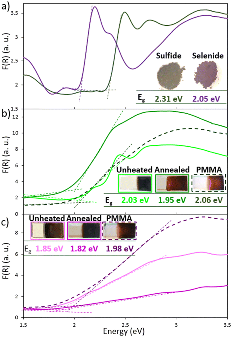 | ||
| Fig. 2 Kubelka Munk transforms of (a) (Bu4N)4[{Re4Mo2Q8}(CN)6] (Q = S, Se) precursor powders and (b) sulfide- and (c) selenide-based films deposited at 40 V for 30 s. For each type of film, the three spectra correspond to the spectra recorded on (i) unheated film, (ii) annealed (T = 200 °C) film and (ii) annealed (T = 200 °C) film covered by PMMA. | ||
This can be attributed to the evolution of energy diagrams induced notably by the mixing of two different metals with different electronegativities and the decrease of the VEC value from 24 to 22 and to a less extent a loss of symmetry compared to the homometallic Re6.
Fig. 3 depicts the evolution of the coloration, the morphology and the thickness of the sulfide-based films according to the applied voltage. From 30 V to 40 V, the thickness of the films increases from 3 to 5 μm and consequently they look darker. Surprisingly, looking at the SEM images, the crystallinity of the layers seems also affected by the increase of the voltage. These observations were then confirmed by the X-ray diffraction analyses. Looking at the X-ray diffraction powder patterns gathered in Fig. 4a and b, it turns out that the X-ray patterns of powders are different from those of deposited films. Moreover, the diffraction peaks at low angles (i.e. around 9.4, 9.9, 11.5 and 12.5°) grow when the applied voltage increases (Fig. S2, ESI†). The deposited surfaces obtained for a voltage of 40 V appear as uniform layers made of 1 μm-size like-octahedral crystals (Fig. 3 and 5a). As far as we know, the growth of Mo6 and Re6-based crystals by EPD without a sintering step was never reported. Conversely, it has been previously observed that the deposition of Mo6 and Re6 clusters leads to amorphous films.3,5,6 The same conclusions can be drawn concerning selenide-based layers. The thickness and the intensity of the color rise by increasing the applied voltage (Fig. S1, ESI†). Crystallized dark brown films until 7 microns thick are obtained for an applied voltage of 40 V for 30 s (Fig. S1, ESI† and Fig. 5b). The microstructure is however finer. Submicronic crystalline phases as in the case of sulfides are not observed. Spherical nanoparticles of about 100 nm in diameter are formed. The diffraction peaks are thus broader than those observed for the sulfide-based layers (Fig. S2, ESI† and Fig. 4b). However, their positions are close and their relative intensities are similar which suggests closely related crystal packing of the cluster units within the layers whatever the nature of the chalcogen. The X-ray diffraction patterns of layers could not be indexed using crystal structures referenced in the databases.
 | ||
| Fig. 3 Photographs and SEM images of the top views and the cross sections of the {Re4Mo2Si8} cluster-based films deposited at various voltages (from 30 to 40 V) for 30 s. | ||
 | ||
| Fig. 4 XRD diagrams of (a) powder ((C4H9)4N)4[{Re4Mo2Si8}(CN)a6] (1′) and corresponding deposited {Re4Mo2Si8} cluster-based films obtained at 40 V for 30 s before and after annealing (T = 200 °C), and (b) powder ((C4H9)4N)4[{Re4Mo2Sei8}(CN)a6] (2′) and corresponding deposited {Re4Mo2Sei8} cluster-based films obtained at 40 V for 30 s before and after annealing. Raman spectra of (c) powder 1′ and the corresponding deposited films before and after annealing, and (d) powder 2′ and the corresponding deposited films before and after annealing. The stars and triangles correspond to the FTO substrate and cluster-based film peaks, respectively. | ||
 | ||
| Fig. 5 Photographs and SEM images of the top views and the cross sections of (a) unheated and (c) annealed at 200 °C for 1 h {Re4Mo2S8} cluster-based films and (b) unheated and (d) annealed at 200 °C for 1 h {Re4Mo2Se8} cluster-based films. All were deposited at 40 V for 30 s. | ||
The vibration spectra and the composition of deposited films were investigated using Raman spectroscopy, EDS and XPS analyses. According to all these complementary techniques, the {Re4Mo2Qi8} cluster cores are preserved during the deposition process. The Raman spectra of the starting powders 1′ and 2′ are globally similar and comparable to those reported in the literature.19 The bands are in the same position (Fig. 4c and d, bands for the sulfides: around 224 and 332 cm−1 (A1g M6), around 410 cm−1 (A1g M–C) and 431 cm−1 (A1g S8) and bands for the selenides: around 237 cm−1 (A1g M6), around 253 cm−1 (A1g M–C) and 285 cm−1 (A1g Se8)). The Raman spectra of the films are similar to those of 1′ and 2′ but some peaks are however broader. This broadening of Raman peaks for the films can be explained by (i) the loss of organization of the cluster units within the layers compared to the more crystallized precursor powder or/and (ii) the loss of symmetry of the cluster units due to the partial substitution of terminal ligands as discussed below. Moreover, one can note that the Raman peaks are broader for the selenide layer, which is less crystallized than the sulfured phase. Comparing the selenide and sulfide films, the XRD peaks are indeed broader too and the particle size is smaller. Although the determination of the chemical composition of Mo, Re and Q by EDS is complex due to the spectra overlap between the Mo L and S K rays, the Re/Mo and (Re + Mo)/Q ratios estimated using this technique do not significantly change for both cluster complexes in 1′ and 2′ and in the films after the deposition (Table S1, ESI†). This finding tends to confirm the conservation of the chemical composition of the cluster cores within the layers. The Re/Mo ratios are 1.6(2) and 1.7(2) respectively for the sulfides and the selenides (theoretical ratio for {Re4Mo2Qi8} = 2). The XPS results are consistent with the Raman and EDS analyses. The peaks corresponding to the Mo and Re contributions (Fig. S3 and S4, ESI†) are similar in positions and relative intensities before and after the deposition for each cluster chalcogenide. No shift due to a possible oxidation process is observed and the metal ratio Re/Mo is preserved (Fig. S3 for the sulfide and Fig. S4 for the selenide, ESI†). The ratios remain relatively constant and close to the theoretical ones of 2 for each chalcogenide (i.e. around 1.9 and 2.3 for the sulfide-based powder and film, respectively, and around 1.6 to 2.3 for the selenide-based powder and film). This confirms that the chemical composition and the oxidation states of the {Re4Mo2Qi8} cluster cores are not modified during the deposition process. Conversely, the decrease and the shift at lower energy of the peaks corresponding to the carbon contribution C 1s (Fig. S3a and S4a, ESI†) and to the nitrogen contribution N 1s (Fig. S3c and S4c, ESI†) in the spectra of the films compared to those of powders 1′ and 2′ indicate the loss of some (C4H9)4N+ counter-cations and/or the apical CN− ligands. If it is difficult for the C 1s peak to be deconvoluted/de-correlated and assigned, two N 1s contributions are observed around 398 and 403 eV. Each contribution found in the XPS spectra of the powders 1′ and 2′ can be attributed, on the one hand, to the nitrogen of CN ligands and, on the other hand, to the nitrogen of the tetrabutylammonium cations. Because of the lower content of tetrabutylammonium (i.e. 4 per unit) compared to the cyanide ligands (i.e. 6 per unit) in the powders 1′ and 2′, the lowest-intensity peak at higher energy (403 eV) can be assigned to the tetrabutylammonium counter-cations and the peak located at lower energy to the cyanide ligands. Comparing the XPS spectra of the powders and those of the films, the concomitant halving of the C 1s and N 1s contributions and the shift of the peak located at 403 eV suggest a loss of two counter-cations. This loss is favored by the deposition process itself. Indeed, due to their opposite charges, the counter-cations and the cluster-based anions migrate in solution in opposite directions. However, the loss of two counter cations leaves open the questions of their charge compensation. In the previous studies performed on Mo6 halides and Re6 chalcohalides,3,5,6 the loss of organic cations was compensated by the substitution of apical halogen ligands (i.e., iodine for Mo6 and chlorine for Re6) by water molecules. This substitution induced a decrease in the charge of the cluster unit without changing its oxidation state. In the present study, the compensation of the loss of tetrabutylammonium cation involves another charge compensation mechanism since the N 1s contribution at 398 eV is very similar in position and in intensity in the spectra of powders and in those of layers. The most plausible scenario is the replacement of two tetrabutylammonium cations by two H3O+. In terms of ligand field theory, the substitution of halogen apical ligands by water molecules observed for [{Mo6Ii8}Ia6]2− and [{Re6Qi8}Cla6] in our previous studies can be explained because the H2O ligand is a stronger ligand field than I− and Cl−. This is not the case in the present study. The CN− groups located in apical positions are stronger ligand fields than water molecules. We assume thus that the loss of two tetrabutylammonium counter-cations among the four ones that counterbalanced the anionic charge of the [{Re4Mo2Qi8}(CN)a6]4− cluster units in 1′ and 2′ is compensated by their replacement by oxonium groups. As previously reported, oxonium groups are generated during the EPD process.3,5,6,14 Consequently, the proposed chemical composition of the {Re4Mo6Qi8} cluster-core-based films is (Bu4N)2(H3O)2[{Re4Mo2Q8}(CN)6]·xH2O (Q = S, Se).
3.3. Electronic and photoconductivity properties
The electronic and photoconductivity properties of the {Re4Mo6Qi8} cluster-core-based films were then investigated by photoelectrochemical characterizations. Due to the instability of the layers in aqueous media, the first photoelectrochemical characterizations were carried out in acetonitrile. Therefore, a solution of KI (6 mmol L−1) and I2 (0.3 mmol L−1) in acetonitrile was used as electrolyte and a classical three-electrode setup, composed of a counter-electrode in platinum, a reference in Ag/AgCl and a cluster-based layer deposited on FTO as the working electrode. Even when the redox couple I−/I3− was inserted in the electrolyte as a redox mediator to favor the photoredox process, the low conductivity of the films limited the intensity of the generated photocurrent. However, although low, the detected photo-responses were sufficient to evaluate the electronic and photoconductivity behaviors of the cluster-based films. The current–potential curves under chopped illumination (Fig. 6a) underlined both photo-oxidation and photo-reduction processes on either side of a photocurrent reversal potential close to the open circuit potential (OCP), namely at 0.1 V and 0.06 V vs. Ag/AgCl for the sulfide and the selenide, respectively. Both photocurrent values are in the same order of magnitude that tends to evidence ambipolar behavior for both films. This is particularly true for the sulfide-based photoelectrode. The cathodic photocurrent is indeed slightly higher than the anodic one for the selenide. Ambipolar behaviors were already observed on Mo6 and Re6 cluster-based films and were explained by the location of the Fermi level close to the middle of the band gap. Similarly, as previously described, the energy level diagram (Fig. 6c) of each chalcogenide layer was established by coupling electrochemical impedance spectroscopy (EIS, see the Mott–Schottky plots in Fig. 6b), UV-vis-NIR (Fig. 2b and c) and XPS measurements (Fig. S5, ESI†).3,16 Thus, the Fermi level was estimated on an absolute energy scale with respect to the vacuum level from the flat band potential value determined by EIS from Mott–Schottky plots (Fig. 6b). The valence band maximum (VBM) was positioned from the difference in energy (ΔE = EF − EVBM) between the VBM and the Fermi level obtained by XPS and the conduction band minimum (CBM) was determined using the band gap value (Eg = ECBM − EVBM). The origin of the ambipolar properties of the sulfide film was clearly evidenced by the relative location of the Fermi level compared to those of VBM and CBM. It pins up to the middle of the band gap. However, the positive slope in the Mott–Schottky (MS) diagram in Fig. 6b (green) underlines the domination of the charge transfer by electrons that is consistent with the OCP evolution under illumination.3,6,20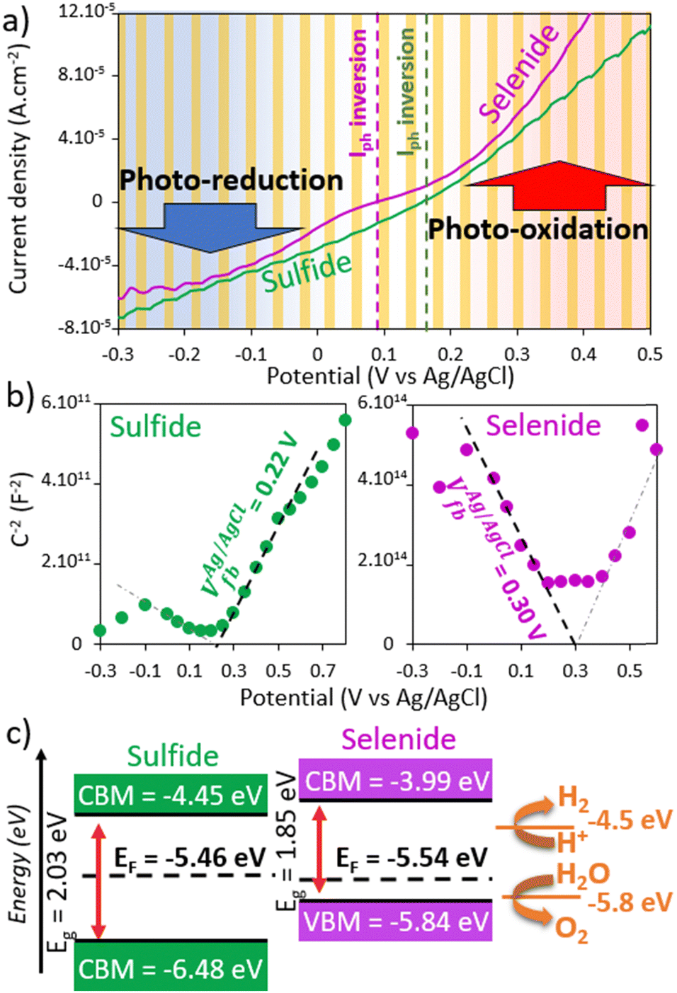 | ||
| Fig. 6 (a) Current–potential curves under chopped illumination of the sulfide (green) and the selenide (purple)-based electrodes. (b) Mott–Schottky (MS) diagrams of those photoelectrodes and (c) corresponding energy diagrams obtained by coupling MS measurements to access the Fermi level position, XPS measurements to obtain the valence band maximum (VBM, Fig. S5, ESI†) and the UV-vis-NIR measurements to position the conduction band minimum (CBM). | ||
Indeed, a decrease of the OCP under illumination (Fig. S6a, ESI†) suggests that the minority charge carriers are holes. Conversely, the photoconductivity of the selenide-based layer appears rather dominated by hole transfer. Its Fermi level is close to the VBM level and the negative slope in the MS plot indicates its p-typeness.3,6,20 The energy diagrams deduced from our measurements are thus consistent with the evolution of the photocurrents versus the potential represented in Fig. 6a (i.e. similar photocurrents for the ambipolar sulfide and higher cathodic photocurrent for the selenide). Those results are comparable to those of {Re6Qi8}-based layers.3 We highlighted an ambipolar behavior with a charge transfer dominated by electron transfer for the Re6 sulfide and a unipolar p-type behavior for the Re6 selenide. In the heterometallic case, the unipolarity of the selenide seems to be more questionable. Indeed, a photo-oxidation current in the same range of magnitude as the photo-reduction current is recorded for potentials higher than the photocurrent reversal potential of 0.06 V vs. Ag/AgCl. Moreover, the OCP decay underlined an n-type behavior (a decrease of the OCP under illumination is observed in Fig. S6b, ESI†) and two slopes can be depicted in the Mott–Schottky plot (Fig. 6b, purple). The presence of surface states or defects in such water molecules can lead to these two different behaviors. Indeed, the surface states control the OCP value that determines the surface charge and thus the depletion or accumulation condition. In the accumulation condition, the reverse band bending leads to a reverse evolution of the OCP under irradiation. For the selenide, the OCP value around 0.08 V vs. Ag/AgCl is just above the reverse potential of 0.06 V vs. Ag/AgCl. For a unipolar compound, no significant photocurrent of majority charge carrier is observed after band bending inversion. As the Fermi level is near to one of the bands (conduction for an n-type and valence for a p-type), the band bending inversion causes a strong reduction (n-type) or oxidation (p-type) current because the Fermi level enters the valence band. The electrodes become thus conductive. Finally, the electronic properties of the Re4Mo2 chalcogenides are globally comparable to those of their Re6 chalcogenide homologues (i.e. similarities in terms of charge carrier domination). However, the photoconductive properties tend towards ambipolarity and thus appear halfway between those of the heterometallic Re6 chalcogenides and Mo6 iodides.
In order to enhance and optimize the interactions between the clusters, the photoelectrodes were annealed at 200 °C for 1 h to remove the trapped water molecules. This strategy was already implemented on Re6 chalcogenide cluster-based films.3 It led to the improvement of the stability under photoelectrochemical measurement conditions and to the increase of the generated photocurrents. UV-vis-NIR, Raman and EDS measurements (Fig. 2 and 4) carried out on annealed films tend to highlight that the chemical composition of the cluster cores does not change after annealing. Indeed, after annealing, the {Re4Mo2Qi8}-based films retain their optical properties. A neglected decrease of the optical band gap is observed (a decrease of 0.08 and 0.03 eV for the sulfide and the selenide, respectively). Although the Raman bands (Fig. 4) appear broader for the sulfide than those recorded on the precursor powders, their frequencies are similar. The Raman peaks of the annealed selenide films are more shaped which highlights the preservation of the vibration mode of the cluster cores. The broadening of the peaks can be attributed to an increase in the disorder and a decrease of the particle size. Indeed, the XRD diagrams (Fig. 4a and b) and the SEM images (Fig. 5) clearly evidenced the disappearance of the crystalline architecture. The XRD peaks at low angles (around 10°, Fig. 4a and b) and the faceted crystals for the sulfide phase are no longer observed after annealing. This results in a thin microstructure built on collapsed nano-sized particles for both chalcogenide layers (Fig. 5c and d). As already observed on Re6-based layers, the thickness of the {Re4Mo2Qi8}-based films slightly decreases by annealing, from 5 to 3 μm for the sulfide and from 7 to 3 μm for the selenide. This suggests a loss of water molecules and a densification of the layers that is consistent with the collapsing observed in the SEM images. This gives them a higher stability. Thanks to the annealing step, photoelectrochemical measurements in aqueous media become now possible. The electrochemical measurements were thus carried out from the same three-electrodes set up as previously described but using a KCl (0.5 M) aqueous electrolyte (Fig. 7a and Fig. S7, ESI†). The comparison with the signal of the FTO substrate alone depicted in Fig. S7 (ESI†) clearly evacuates the contribution of the substrate. For both chalcogenide-based photoelectrodes, a photocurrent inversion potential is observed (Vinv are around −0.08 V and 0.29 V vs. Ag/AgCl for the sulfide and the selenide-based photoelectrodes) with similar values of photo-oxidation and photo-reduction current density that evidences ambipolar properties. With positive slopes, MS measurements (Fig. 7b) however highlighted the domination of the charge transfer by electrons. If this tendency is similar for the sulfide-based layers before and after annealing, a reverse electronic behavior is observed for the selenide ones. In that case, the annealing seems to increase to the electron concentration in the films that modifies the nature of minority charge carriers. It turns out that this modification of the electronic behavior of the selenide-based film after annealing originates from a shift in its Fermi level at higher energy (Fig. 7c). Indeed, the flat band potential values determined using the MS method (Fig. 7b) are lower for both annealed films that cause a shift in higher energies of EF (less negative) around 0.5 eV. This evolution of electronic properties affects the relaxation kinetics of photogenerated charge carriers too. Indeed, the lifetime of the photoexcited electron determined by fitting the OCP decay curves in Fig. S6 (ESI†) is longer after annealing which supposes a lower recombination rate and indicates more efficient photoelectrodes. The impact of the annealing appears weaker for the sulfide even if the values of the photo-reduction currents seem slightly lower than those of the photo-oxidation currents. In both cases, the lower values of the slope translate into an increase in the charge carrier density into the films and, possibly, of their conductivity too. The lower slope for the sulfide may indicate a higher charge carrier density.
 | ||
| Fig. 7 (a) Current–potential curves under chopped illumination of the annealed (T = 200 °C) sulfide (green) and selenide (purple)-based electrodes. (b) Mott–Schottky (MS) diagrams of such photoelectrodes and (c) comparison of the estimated Fermi level positions of such annealed electrodes (orange) with the unheated ones (grey). | ||
The photoconductivity properties of the homometallic rhenium cluster-based photoelectrodes were reported in a previous publication.3 Promising photoredox activities in water were thus highlighted. Herein, a deeper study was carried out on the heterometallic {Re4Mo2Qi8}-based photoelectrodes. The origin of the photocurrent in water may involve the reduction of water along with its oxidation. Indeed, as underlined in Fig. 6c, the position of energy levels of {Re4Mo2Qi8}-based layers are in agreement with both water photo-oxidation and water photo-reduction. Thus, the photo-reduction and the photo-oxidation currents were studied under standard conditions using a phosphate buffer solution (pH 7) and a solar simulator (AM1.5). A neutral pH was chosen in order to help the stabilization of the layers and limit the release or corrosion effects. On one hand, the current–potential curves in Fig. 8 and Fig. S8 (ESI†) depict the evolution of the cathodic (Fig. 8a and b) and anodic (Fig. S8a and b, ESI†) current densities with and without light irradiation for each chalcogenide-based photoelectrodes. On the other hand, the chonoamperometry curves recorded at 0.2 V (Fig. 8c and d) and 1.4 V (Fig. S8c and d, ESI†) vs. RHE highlight the stability of the reduction and oxidation photocurrents. The applied potentials were chosen in order to limit the cluster release. The cathodic photocurrent probably corresponds to the water reduction leading to the H2 production assisted by sunlight whereas the anodic photocurrent probably corresponds to the water oxidation leading to the O2 production. It turns out that the transient photocurrent densities, in reduction and in oxidation, generated by both types of chalcolgenide photoelectrodes are globally comparable. Although the absorption properties are more favourable for the selenide (i.e. bandgaps of 1.82 eV and 1.95 eV for the selenide and the sulphide, respectively), the photo-reduction current values are slightly higher from the sulfide-based photoelectrodes. This can be explained by the higher charge carrier density and probably the superior conductivity of the sulfide-based films. However, certainly due to the slower relaxation kinetics of charge carriers, the global photocurrent generated by the selenide-based photoelectrodes is similar and even higher after 1 h of illumination compared with the sulfide ones. A reverse trend is observed on the anodic side, and the photocurrent generated by selenide-based photoelectrodes is higher by about one order of magnitude. The chronoamperometry at 1.4 V vs. RHE (Fig. S8c and d (ESI†)) however, highlights the instability of the photocurrent. After a strong increase (first part of the amperometry curves in Fig. S8c and d, ESI†), the photocurrent rapidly decreases after 20 s of illumination that is concomitant with a deterioration of the layer. In order to limit the degradation of the photoelectrodes, a coating of a polymer, namely poly(methylmethacrylate) (PMMA), was deposited on the topside of the chalcogenide-based layers. The optical properties are preserved (Fig. 2b and c) and the stability of the layers was improved while limiting the decrease of the photocurrent due to the higher resistivity of the film brought by the isolating PMMA layer (Fig. S8c and d, ESI†). No strong corrosion currents are observed with the PMMA protection (Fig. 8c, d and Fig. S8c, d, ESI†). The anodic (at 1.4 V vs. RHE) and cathodic (at 0.2 V vs. RHE) photocurrents, around 10 μA cm−2 for both chalcogenide-based photoelectrodes, stay stable for more than 8 h (Fig. S9, ESI†) which corresponds to the longest time of measurement.
 | ||
| Fig. 8 Current–potential curves and chronoamperometry at 0.2 V vs. RHE in the dark (dashed lines) and under illumination (solid lines) obtained from the annealed (T = 200 °C) (a) and (c) sulfide (green) and (b) and (d) selenide (purple)-based electrodes. (a) and (b) were obtained under chopped illumination and (c) and (d) under constant illumination. | ||
These values are far below the best photogenerated current values reported on QD-based photoelectrodes that are greater than a few mA cm−2 to more than 10 mA cm−2.20 However, the onset reduction potential values around 0.3–0.5 V vs. RHE with current densities around 0.2 mA cm−2 at 0 V vs. RHE highlight promising electro- and photoelectrocatalytic activities. Due to the increase of the Fermi level with the annealing, the energy barrier between EF and the redox level of the couple H+/H2 is decreased which favours the water reduction. Thus, (electro)catalytic and photo(electro)catalytic processes seem to contribute to the faradaic current. Moreover, these photocurrent values were obtained on thick resistive layers in which the cluster chalcogenides are not strongly bonded, which favours the charge recombination and the reloading of clusters in solution. This is the first proof of concept and the charge transfer processes need to be improved by designing cluster-based photoelectrodes to fully characterize the photo-water splitting efficiency of such systems. The chemisorption of thin layers on nanostructured semiconducting oxide-based electrodes like QD-based photoelectrodes or the design of heterojunctions should improve the performance of these systems.3,21,22 It is also worth emphasizing that the photocurrent values obtained under the same conditions are increased by almost one order of magnitude compared to those reported on homometallic Re6 chalcogenide-based photoelectrodes in the previous study.3 The values of photocurrent at 0 V vs. Ag/AgCl were around 0.47 and 1.3 μA cm−2 for {Re6Si8}- and {Re6Sei8}-based photoelectrodes, respectively, and are around 50 and 20 μA cm−2 for {Re4Mo2Si8}- and {Re4Mo2Sei8}-based photoelectrodes, respectively. Mixing Re and Mo metal atom within the same heterometallic octahedral cluster clearly exalts the photoconductive properties.
4. Conclusion
To sum up, as new advances in the use of metal atom clusters in the design of photoelectrodes, the photoconductivity properties of heterometallic {Re4Mo2Qi8} (Q = S or Se) chalcogenides were investigated. Photoelectrodes were prepared by deposition of {Re4Mo2Qi8} cluster-based films onto FTO substrates using an electrophoretic deposition technique with solutions of the salts (Bu4N)4[{Re4Mo2Qi8}(CN)a6] (Q = S, Se). The resulting (Bu4N)2(H3O)2[{Re4Mo2Qi8}(CN)a6]·xH2O (Q = S, Se)-based crystalline films are composed of crystals whose sizes range from a hundred nanometers for the selenide phase to a few microns for the sulfide. This is the first time that the growth of M6 (M = Mo and Re) cluster-based crystals using an EPD process has been reported. The photoconductivity properties of such (Bu4N)2(H3O)2[{Re4Mo2Qi8}(CN)a6]·xH2O (Q = S, Se)-based films were then investigated through (photo)electrochemical characterizations. Ambipolar behavior was evidenced for both S and Se chalcogenides. However, in accordance with the previous results obtained on Re6-based films, the charge transfer is dominated by electrons in the sulfide film and, reversely, by holes in the selenide film. The stability in water and the photoconductivity properties are improved by an annealing step at 200 °C. This annealing step allows expelling the water molecules trapped inside the layers between the cluster-based units. Therefore, the interactions between the clusters inside the layers are enhanced that improves thus the density of charge carriers and the conductivity. For both chalcogenide cluster-based films, the Fermi level migrates towards the higher energies after annealing. Although still ambipolar, the charge transfer is dominated by the electrons whatever the chalcogenide. The influence of both the chemical compositions and of the strength of interactions between clusters on their optical and electronic properties was highlighted. They can be controlled by using the nanoarchitectonics starting from discrete molecular clusters to form layers that are better organized. Compared to previous works, the mixing of rhenium and molybdenum atoms within the same heterometallic clusters enables not only the optical properties and transport properties within the active layers to be optimized, but it also enables the positions of the energy levels to be tuned. Indeed, the origin of the photocurrents in water rely on the reduction and the oxidation of water owing to favourable alignment of the HOMO and LUMO energy levels of {Re4Mo2Qi8}@FTO-based photoelectrodes with those of reductions of protons and oxidation of water. The photo-reduction and photo-oxidation processes were then investigated under standard conditions at pH 7. The chalcogenide-based films are more stable under cathodic conditions. However, a PMMA protection allows generating stable photo-reduction and also photo-oxidation currents for more than 8 h. This study opens the door to the development of new cluster-based photoelectrodes, namely photocathodes but also photoanodes, by coupling clusters with various compositions, for the photoelectrochemical water splitting.Conflicts of interest
There are no conflicts to declare.Acknowledgements
The authors thank the CMEBA platform (Francis Gouttefangeas and Loic Joanny) from UMS 2001 ScanMAT CNRS-Université Rennes 1 for the FE-SEM images and analyses. Raman's investigations were performed using facilities available on SIR Platforms from UMS 2001 CNRS-Université Rennes 1 (Fig. S2, ESI†). The authors are very grateful to Bertrand Lefeuvre ISCR UMR 6226 CNRS-Université Rennes. The authors thank Rennes Metropole for its financial support via the AIS funding. The International Associate Laboratory CLUSPOM (2018–2023) is acknowledged for financial support as well as the French Embassy in Moscow to support a Verandsky grant for T. I. Lappi. Naumov N. G., Lappi T. I. and Gayfulin Y. M. are grateful that the research was also supported by the Ministry of Science and Higher Education of the Russian Federation. The co-author thanks the ANR for its financial support through the NanoLEtsGOs project (ANR-22-CE09-0015).References
- F. A. Cotton, Inorg. Chem., 1964, 3, 1217 CrossRef CAS.
- L. R. Long, L. C. McCarty and R. H. Holm, J. Am. Chem. Soc., 1996, 118, 4603 CrossRef.
- T. I. Lappi, S. Cordier, Y. M. Gayfulin, S. Ababou-Girard, F. Grasset, T. Uchikoshi, N. G. Naumov and A. Renaud, RRL Solar, 2023, 7, 2201037 CrossRef CAS.
- K. Kirakci, S. Cordier and C. Perrin, Z. Anorg. Allg. Chem., 2005, 631, 411 CrossRef CAS.
- A. Renaud, T. K. N. Nguyen, F. Grasset, M. Raissi, V. Guillon, F. Delabrouille, N. Dumait, P.-Y. Jouan, L. Cario, S. Jobic, F. Odobel, S. Cordier and T. Uchikoshi, Electrochim. Acta, 2019, 317, 737 CrossRef CAS.
- A. Renaud, P.-Y. Jouan, N. Dumait, S. Ababou-Girard, N. Barreau, T. Uchikochi, F. Grasset, S. Jobic and S. Cordier, ACS Appl. Mater. Interfaces, 2022, 14, 1347 CrossRef CAS PubMed.
- T. K. N. Nguyen, C. Lebastard, M. Wilmet, N. Dumait, A. Renaud, S. Cordier, N. Ohashi, Y. Uchikoshi and F. Grasset, Sci. Technol. Adv. Mater., 2022, 23, 547 CrossRef PubMed.
- K. Ariga, Nanoscale Horiz., 2021, 6, 364 RSC.
- A. Renaud, L. Cario, X. Rocquefelte, P. Deniard, E. Gautron, E. Faulques, T. Das, F. Cheviré, F. Tessier and S. Jobic, Sci. Rep., 2015, 5, 12914 CrossRef PubMed.
- H. Lu, J. Tournet, K. Dastafkan, Y. Liu, Y. H. Ng, S. K. Karuturi, C. Zhao and Z. Yin, Chem. Rev., 2021, 121, 10271 CrossRef CAS PubMed.
- C. Xu, P. R. Anusuyadevi, C. Aymonier, R. Luque and S. Marre, Chem. Soc. Rev., 2019, 48, 3868 RSC.
- Y. Ren, S. Han and Y. Zhou, in Ambipolar Materials and Devices, ed. Y. Zhou and S. Han, Royal Society of Chemistry, 2020, pp. 1–13 Search PubMed.
- S. Z. Bisri, C. Piliego, J. Gao and M. A. Loi, Adv. Mater., 2014, 26, 1176 CrossRef CAS PubMed.
- T. K. N. Nguyen, A. Renaud, B. Dierre, B. Bouteille, M. Wilmet, M. Dubernet, N. Ohashi, F. Grasset and T. Uchikoshi, Bull. Chem. Soc. Jpn., 2018, 91, 1763 CrossRef.
- T. I. Lappi, Y. M. Gayfulin, A. Renaud, C. Prestipino, P. Lemoine, V. V. Yanshole, V. K. Muravieva, S. Cordier and N. G. Naumov, Molecules, 2023, 28, 5875 CrossRef CAS PubMed.
- V. K. Muravieva, Y. M. Gayfulin, C. Prestipino, P. Lemoine, M. R. Ryzhikov, V. V. Yanshole, S. Cordier and N. G. Naumov, Chem. – Eur. J., 2019, 25, 15040 CrossRef CAS PubMed.
- P. Bais, M. T. Caldes, C. Guillot-Deudon, A. Renaud, M. Boujtita, S. Jobic and A. Lafond, Mater. Res. Bull., 2021, 139, 111285 CrossRef CAS.
- M. Y. Gorina and D. K. Kollerov, Meas. Tech., 1974, 17, 135 CrossRef.
- T. G. Gray, C. M. Rudzinski, E. E. Meyer, R. H. Holm and D. G. Nocera, J. Am. Chem. Soc., 2003, 125, 4755 CrossRef CAS PubMed.
- A. W. Bott, Curr. Sep., 1998, 17, 87 CAS.
- L. Jin, H. Zhao, Z. M. Wang and F. Rosei, Adv. Energy Mater., 2021, 11, 2003233 CrossRef CAS.
- Y.-C. Lin, L.-C. Hsu, C.-Y. Lin, C.-L. Chiang, C.-M. Chou, W.-W. Wu, S.-Y. Chen and Y.-G. Lin, ACS Appl. Mater. Interfaces, 2019, 11, 38625 CrossRef CAS PubMed.
Footnote |
| † Electronic supplementary information (ESI) available. See DOI: https://doi.org/10.1039/d3tc04635d |
| This journal is © The Royal Society of Chemistry 2024 |