
 Open Access Article
 This Open Access Article is licensed under a
 Creative Commons Attribution 3.0 Unported Licence
Transfer-printing of patterned PEDOT:PSS structures for bendable, stretchable and biodegradable electronics†
Carla
Volkert
*a,
Renan
Colucci
 a,
Rüdiger
Berger
b,
Pol
Besenius
c,
Paul W. M.
Blom
d and
Ulrike
Kraft
*a
a,
Rüdiger
Berger
b,
Pol
Besenius
c,
Paul W. M.
Blom
d and
Ulrike
Kraft
*a
aOrganic Bioelectronics Research Group, Max Planck Institute for Polymer Research, Mainz 55128, Germany. E-mail: volkertc@mpip-mainz.mpg.de; kraftu@mpip-mainz.mpg.de
bDepartment of Physics at Interfaces, Max Planck Institute for Polymer Research, Mainz, Germany
cDepartment of Chemistry, Johannes Gutenberg Universität Mainz, Mainz 55128, Germany
dDepartment of Molecular Electronics, Max Planck Institute for Polymer Research, Mainz 55128, Germany
First published on 16th February 2024
Abstract
The conductive polymer poly(3,4-ethylenedioxythiophene):poly(styrene sulfonate) (PEDOT:PSS) is of great interest for a variety of applications in flexible and stretchable electronics, due to its high conductivity, optical transparency, mechanical properties, commercial availability and biocompatibility. However, to advance novel applications on conformable substrates, the development of innovative and reliable methods for processing conductive polymers is vital. Here, a fast, dependable and easy PEDOT:PSS transfer-printing method onto flexible, transparent and biodegradable poly(vinylalcohol) (PVA):glycerol targets is presented. In contrast to previous work, this method neither depends on acid, nor doping, nor surface soaking treatments. Furthermore, this approach is compatible with common strategies to induce stretchability and increase the conductivity of PEDOT:PSS. To ensure the applicability to next-generation flexible and stretchable electronics, the electrical, morphological and adhesion properties before and after printing are characterized. Additionally, a straightforward methodology to pattern transfer-printable PEDOT:PSS structures is established, using an O2-plasma treatment. Furthermore, the water-soluble targets allow for environmental-friendly disposal.
 Ulrike Kraft | Ulrike Kraft is an Independent Research Group leader at the Max Planck Institute for Polymer Research in Mainz, Germany within the Lise Meitner Excellence Program. She obtained her PhD at the MPI for Solid State Research in Stuttgart, which was followed by two postdoctoral stays at Stanford University and at the University of Cambridge. Dr Kraft and her group are working at the intersection between Chemistry, Physics and Materials science, focusing on organic electronic materials, the charge transport through these materials and their application in flexible and stretchable electronic devices such as organic transistors and biosensors. |
Introduction
Flexible and stretchable electronic devices and circuits offer high prospects for applications in mobile, wearable and on-skin electronics, personalized medicine and biomonitoring. Hence, enormous efforts are attributed to develop conformable devices such as biosensors,1 optoelectronic devices,2 organic field effect transistors (OFETs),3,4 light emitting diodes (LEDs)5 and organic electrochemical transistors (OECTs).6–8 To realize next-generation electronics, a change from rigid to flexible and stretchable components is required and calling for new device fabrication processes as well as flexible and stretchable electronic materials including substrates and (transparent) conductors. Additionally, defined structuring of the latter material is crucial to pattern electrodes and functional devices.As a material the conducting organic polymer poly(3,4-ethylenedioxythiophene): polystyrene sulfonate (PEDOT:PSS) is a popular choice, due to its optical transparency, mechanical properties, high conductivity, commercial availability and biocompatibility.9–11 It consists of positively charged PEDOT-chains and negatively charged PSS-chains. Within the polymer, PSS serves as a dopant and counter-ion for PEDOT and enables the dispersion of PEDOT in water which itself is water-insoluble. Pristine PEDOT:PSS films exhibit a conductivity of approximately 1 S cm−1. Hence, various treatments, such as doping via polar solvents, strong acids or ionic liquids are commonly employed to increase the conductivity to hundreds or even thousands of S cm−1.6,10,12 Extensive research has been attributed to investigate the underlying mechanisms behind this increased conductivity of PEDOT:PSS. In general, the following factors are discussed to play a role in the conductivity enhancement: A change in the PEDOT-resonant structure from benzenoid to quinoid, a change in conformation from coil to extended-coil, a change in grain size, separation between PEDOT-rich and PSS-rich phases as well as secondary doping and charge screening effects.10,13
In terms of flexible and stretchable substrates various materials such as polyethylene terephthalate (PET),14 styrene ethylene butylene styrene (SEBS)3,15 or polydimethylsiloxane (PDMS)16 are commonly employed. However, the deposition of PEDOT:PSS thin-films e.g. through spin-coating on flexible plastic substrates faces difficulties for several reasons: First, the adhesion of PEDOT:PSS to hydrophobic flexible and stretchable substrates is generally poor,2 making it difficult to produce uniform films and leading to delamination. In addition, flexible and stretchable plastic substrates are prone to be damaged by harsh treatments commonly employed to increase the conductivity of PEDOT:PSS, such as acid treatments.2
An elegant approach to avoid these problems is transfer-printing, which allows e.g. acid washing and soaking on glass substrates prior to the transfer to the final soft substrates. The respective process involves lifting a spin-coated thin-film from a glass substrate and placing it onto a target substrate with or without the use of a transmission substrate.2,14,17–19 To make transfer-printing successful, adjusting the PEDOT:PSS adhesion is key. It is possible to either reduce the adhesion on the donating substrate or increase it on the receiving substrate. For this purpose, (chemical) treatment of the PEDOT:PSS,2,17,20 the target substrate,16 or both simultaneously14 are reported. Common treatments to increase the conductivity of PEDOT:PSS and simultaneously decrease its adhesion to the donating glass substrate include the addition of surfactants20 and acid treatment of PEDOT:PSS films.2,17 Treatments of the receiving substrate to increase the adhesion of PEDOT:PSS include chemical functionalization (e.g. of PDMS16) and the employment of hydrogen bonds. Combining different approaches allows the optimization of the adhesion at multiple steps. For example Fan et al.14 performed a methanesulfonic acid-treatment on PEDOT:PSS films and furthermore spin-coated a PEDOT:PSS/D-sorbitol mixture on the receiving PET substrate to form hydrogen-bonds with the later on transferred PEDOT:PSS. All of these approaches are limited in their applicability as they depend on specific chemicals or treatments. To date, a widely applicable approach that enables the processing of variously treated PEDOT:PSS thin films on stretchable and flexible substrates is missing.
For the application of PEDOT:PSS as electrodes as well as active layer in functional electronic devices such as OECTs, patterned structures are crucial.21 Common routes to structure PEDOT:PSS often require complicated protocols or lead to low conductivities.21,22 In general, they can be divided into post-deposition approaches such as (photo)lithography23 and direct patterning strategies including screen printing,24 inkjet-printing15,25 and electrochemical deposition.26,27 A simplified approach for photo-patterning PEDOT:PSS without the need for etching and the removal of residual photoresist, introduces photopolymerizable additives into PEDOT:PSS. Photomasks and irradiation followed by washing yield micron-sized PEDOT:PSS patterns.21,28,29 An opposite strategy fine-tunes the interface chemistry of the substrate, so that PEDOT:PSS only adheres in specified areas.30 Another approach attaches a mask to rubbery substrates prior to the spin-coating of PEDOT:PSS.8,16 Lastly, PEDOT:PSS may be patterned employing a multi-step etching process31 as reported by Kostanovskii et al. who deposited copper patterns onto a PEDOT:PSS thin-film, requiring post-patterning acid treatments to remove the residual copper. All the strategies presented above require specific chemicals, lengthy protocol or expensive equipment, underscoring the need for straightforward and easy methods to reliably pattern PEDOT:PSS thin films.
Here, we report an easy and reliable route to transfer (patterned) PEDOT:PSS to flexible and stretchable substrates. The presented transfer-printing employs biodegradable32 poly(vinylalcohol) (PVA) in combination with the plasticizer glycerol as a flexible and stretchable substrate. To transfer the PEDOT:PSS thin-films, a novel printing method is presented. This method is compatible with common ways of increasing the conductivity and makes use of the creation of hydrogen bonds between PVA, glycerol and PEDOT:PSS. Upon transfer the conductivity is maintained and within the range of literature values. The samples were furthermore examined in detail using PeakForce Quantative Nanomechanical mapping (PF-QNM). Additionally, we demonstrate an extremely easy route towards patterned and transfer-printable PEDOT:PSS structures via O2-plasma treatment. The work presented here will highly facilitate the processing of next-generation flexible and stretchable electronics.
Results and discussion
Transfer-printing
For the newly established transfer-printing process (illustrated in Fig. 1a), the flexible and stretchable target substrates and the conducting thin-films (PEDOT:PSS) are prepared separately. The substrates consist of the polymer PVA and glycerol as plasticizing additive (see Fig. 1d for chemical structures). PVA is an attractive candidate for substrates in stretchable electronics as it provides several advantages: First of all, hydrogels in general are attractive candidates for healthcare applications in close contact with the human body, due to their high water content, mechanical softness, biocompatibility and biofunctionality.33 Additionally, PVA is approved by the American Food and Drug administration (FDA) for various medical applications.33 By incorporating glycerol in varying amounts, the mechanical and optical properties of the substrates can be adjusted by tuning the free volume within the polymer.32,34,35 This versatility allows access to systems with specifically tailored shapes and mechanical properties for various kinds of applications. To prepare the target substrates, PVA, glycerol (25 wt%) and deionized (DI) water were combined in the appropriate amounts and stirred for three hours at 90 °C to ensure the dissolving of the PVA. The resulting mixtures were drop-cast onto pre-cleaned glass slides and peeled-off after drying. Due to the good film-forming properties of PVA,34–36 the PVA:glycerol mixture can be applied to any type of glass slide and additionally cut into the desired shape after drying. The resulting films are displayed in Fig. 1c and a video demonstrating the transfer-printing process can be found in the EIS (video S1, ESI†). The films are transparent and may easily be stretched, twisted and bent. PEDOT:PSS thin-films were prepared via spin-coating. To ensure that the printing is compatible with common approaches to increase the conductivity, the transfer-printing of variously treated as well as pristine PEDOT:PSS (PH1000 and AI4083) films was tested to ensure the compatibility with a variety of applications. The examined treatments include the combined incorporation of ethylene glycol (EG) and dodecylbenzene sulfonic acid (DBSA)37 (pre-deposition) and acid treatments using methansulfonic acid2 and sulfuric acid2 as well as DMSO soaking12 (post-deposition). After the preparation of the PEDOT:PSS films, the PVA/glycerol substrates were applied onto the PEDOT:PSS thin films. Mild heat facilitates the removal from the donating substrate. Key to this transfer-printing approach are hydrogen bonds formed between the PVA:glycerol target substrates and the polymer PEDOT:PSS14,20 as schematically indicated in Fig. 1a and d. Hence, the adhesion for any tested PEDOT:PSS-treatment has to be lower to the donor glass substrate than to the target PVA:glycerol substrate, enabling a smooth transfer. A previously reported excess of hydrophilic PSS that is forming at the top of spin-coated PEDOT:PSS thin films38,39 might also be beneficial for the transfer-printing process as suggested in40 and schematically indicated in Fig. 1d. In general, transferring large areas of film is challenging as cracks can form easily.17,41 Using the here reported methodology, however, it is possible to transfer films with an area of at least 7.5 × 2.5 cm. Furthermore, this approach is applicable to a wide range of PEDOT:PSS film thicknesses: Fig. 1e shows the respective donating substrates as well as transferred films from drop-casted to spin-coated PEDOT:PSS films (drop-casted: 2.8 μm; spun at 500 rpm: 120 nm and at 1000 rpm: 70 nm).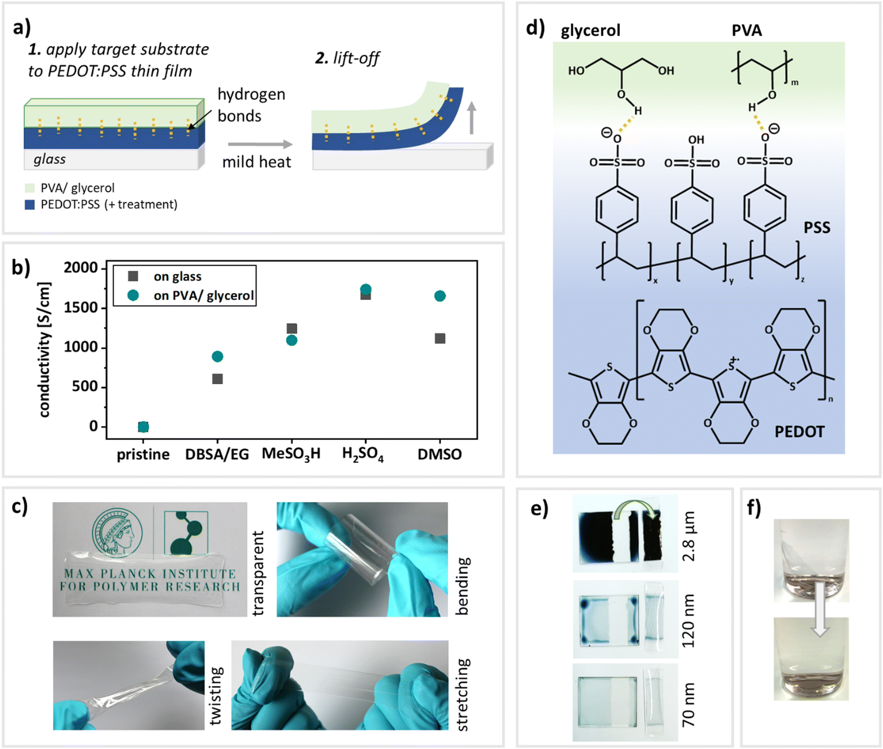 | ||
| Fig. 1 (a) Schematic illustration of the transfer-printing process. (b) Comparison of electrical conductivities of variously treated PEDOT:PSS thin-films on glass and PVA:glycerol substrates. (c) PVA:glycerol (25 wt%) substrates are transparent, bendable, twistable and stretchable. (d) Schematic drawing of the formation of hydrogen bonds between glycerol, PVA and PEDOT:PSS, which enables the transfer-printing process. (e) Transfer-printing PEDOT:PSS with different thicknesses. (f) Dissolving the PVA:glycerol/PEDOT:PSS samples in water for environmental-friendly disposal. | ||
In summary, the transfer-printing method presented here is not dependent on acids2,17 or surfactant and/or doping treatments,2,14,17,20 is applicable to various film thicknesses and, unlike previously reported methods,20 pristine thermally annealed PEDOT:PSS film may be transferred as well. Please see Table S1 for a comparative overview of various transfer-printing techniques onto flexible and stretchable target substrates (ESI†), pointing out the advantages this methodology offers. Lastly, the PVA substrates are water-soluble and allow for environmentally friendly disposal by employing mild heat and stirring (Fig. 1f).
Properties of transfer-printed films
To make full use of the transfer-printed PEDOT:PSS films in electronic applications, they need to maintain their electrical properties during the transfer process. Hence, the conductivity of variously treated PEDOT:PSS thin-films was measured prior to and after the transfer via two point probe measurements. Table 1 compares the conductivities of reported literature values, the reproduced process on glass slides and the transfer-printed films on PVA:glycerol (25 wt%) substrates. A graphical comparison is given in Fig. 1b. Please note that for the assurance of process functionality, for each treatment an identical thin film was assessed both before and after transfer-printing. Furthermore, to demonstrate reproducibility, the same procedure was conducted on six individual samples of PEDOT:PSS treated with DBSA and EG (Fig. S1, ESI†). It is furthermore noteworthy that for PEDOT:PSS AI4083 recording a resistance value was not possible due to too low currents (on glass as well as PVA:glycerol). Therefore, we have recorded and attached a video demonstrating the transfer-printing (video S1, ESI†). As expected, the pristine PEDOT:PSS shows a conductivity of only a few S cm−1, while the pre- and post-deposition treatments lead to a significant increase in conductivity. We would like to point out that the aim of this work is not the full optimization towards the highest possible conductivities, but rather to verify that the electronic properties are maintained during the transfer. The conductivities in our work are either identical or slightly lower than the values reported in literature. However, most importantly, the initial conductivity of PEDOT:PSS on glass is maintained during the transfer process and very similar on glass and on PVA:glycerol (25 wt%) substrates for all treatments, demonstrating the versatility of the process. Interestingly, the transferred films on the stretchable PVA:glycerol substrates oftentimes even yield higher conductivities than initially on glass substrates. This may be caused by doping effects from the glycerol.10,42 We conclude that the electrical properties of the thin films are not impaired by the transfer-printing process or might in fact even be enhanced.| Conductivity [S cm−1] | Surface roughness [nm] | Adhesion force [nN]a | |||||
|---|---|---|---|---|---|---|---|
| Literature on glass | on glass | on PVA: glycerol (25 wt%) | on glass | on PVA: glycerol (25 wt%) | on glass | on PVA: glycerol (25 wt%) | |
| a between the sample and the SFM-tip surface extracted from PeakForce SFM measurements. | |||||||
| PEDOT:PSS | 2.512 | 0.5 | 0.8 | 1.4 | 1.0 | 5.2 | 0.92 |
| + DMSO | 212412 | 1600 | 1655 | 1.6 | 1.4 | 0.9 | 0.29 |
| + H2SO4 | 28302 | 2808 | 2976 | 3.0 | 1.2 | 2.2 | 0.28 |
| + DBSA/EG | 80037 | 797 | 927 | 1.3 | 1.7 | 1.9 | 0.25 |
| + MeSO3H | 30902 | 1348 | 1860 | 2.7 | 1.3 | 2.3 | 1.0 |
Since transparency may also be a prerequisite for certain applications43 such as optoelectronic devices it should be maintained during the transfer process. Within the visible spectrum, the transmittance of all PEDOT:PSS thin-films after transfer-printing onto PVA:glycerol remains well above 95% compared to the value obtained for PEDOT:PSS thin-films on glass (Fig. S3 and Table S3, ESI†). Hence, our methodology enables the fabrication of highly conductive, reaching almost 3000 S cm−1 (Table 1), and transparent PEDOT:PSS thin-films on flexible and stretchable substrates.
When envisioning future applications and for a full characterization of the transfer-printed films, insight into the surface morphology is crucial. Therefore, we performed a detailed study of the morphological and mechanical properties of the thin films before and after transfer-printing, performing scanning force microscopy (SFM) measurements applying peak-force mode. In this mode, we simultaneously map the adhesion between the SFM-tip and the sample surface and deformation of the film corresponding to its mechanical properties.44 These properties provide further insight into a material beyond pure topological information. To the best of our knowledge there are only few reports on pre- and post-treated PEDOT:PSS thin-films on flexible substrates.17,45–47 Additionally, these images were acquired in tapping mode and a detailed SFM adhesion study of variously treated PEDOT:PSS thin films is still lacking. All PEDOT:PSS thin films on glass exhibit a surface roughness in the order of a few nanometers (Fig. 2). The roughness values extracted from several images of an area of 1 μm × 1 μm indicate smooth surfaces (Table 1). In the corresponding adhesion force maps (greenish color scale, Fig. 2) we observe a contrast, which we attribute to a core–shell structure of PEDOT:PSS. A core–shell morphology is commonly reported in literature.17,45,46,48–53 Taking the morphology into account, we assign the dark green areas (lower adhesion forces) to the PEDOT-rich cores and bright areas (higher adhesion forces) to the PSS-rich shells. In SFM images recorded in tapping mode it is generally assumed that bright areas (positive phase shift of the oscillating cantilever) correspond to PEDOT-rich and dark areas to PSS-rich regions.45,50,54 A comparison of the adhesion maps of treated and untreated PEDOT:PSS thin films reveals a reduction of the grain size caused by post-deposition acid treatments with diluted MeSO3H (40%) or H2SO4 (18%), which is consistent with literature.17,48,51,55 In our recordings, this reduction in grain size is also observed for DMSO post-deposition treatments, whereas the grains appear to be more elongated and oval-shaped upon the addition of DBSA/EG. We calculated the mean adhesion force values for all surfaces (see Table 1). The average adhesion decreases with increasing conductivity. This may be attributed to the content of PSS in the PEDOT:PSS films upon conductivity-enhancing treatments as reported previously.50,53
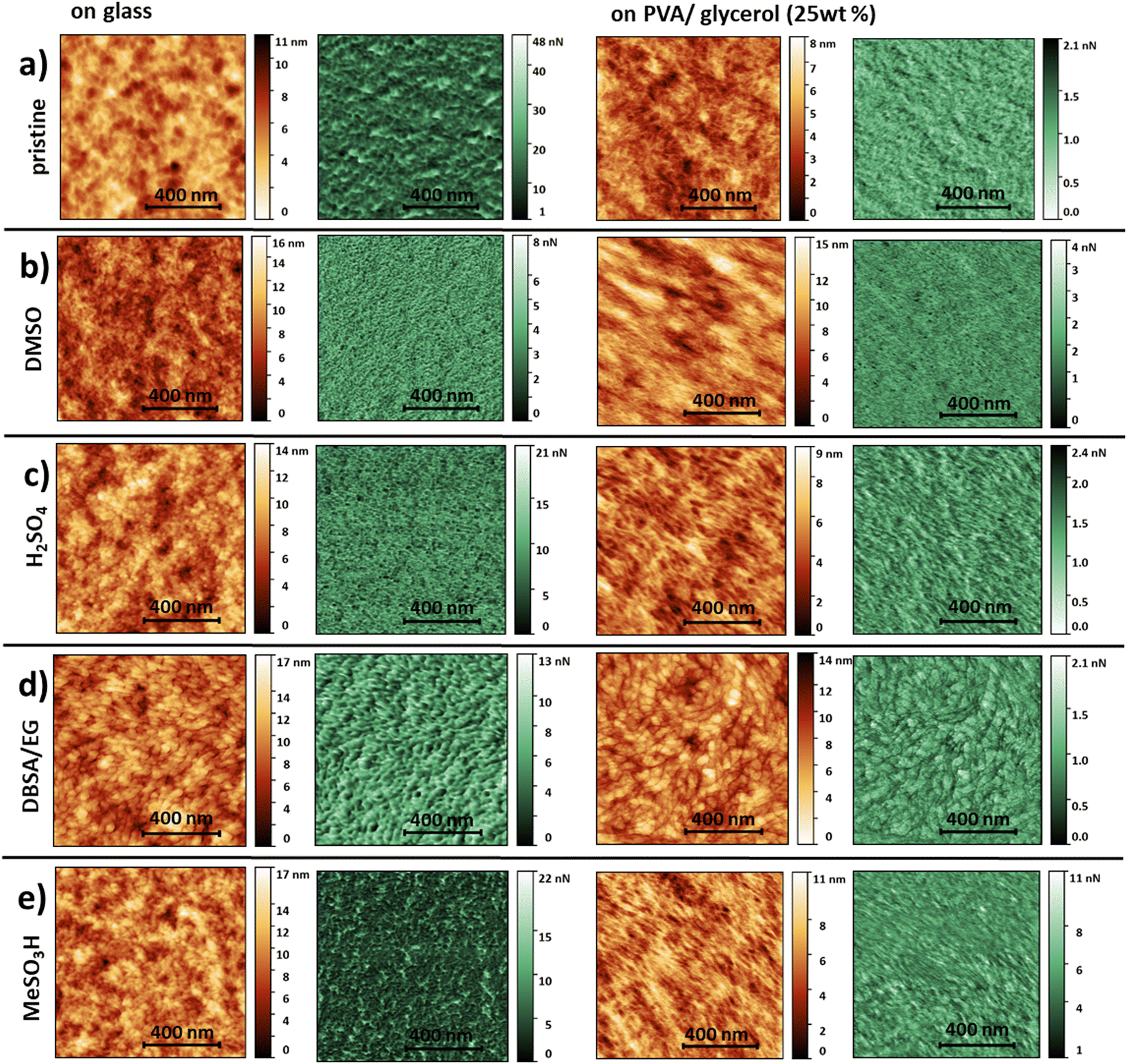 | ||
| Fig. 2 SFM images recorded in Peak Force mode. We selected an orange color scale for topography and a green color scale for the corresponding adhesion forces. (a) pristine (PH1000), (b) DMSO12-, (c) H2SO42-, (d) DBSA/EG37- and (e) MeSO3H2-treated PEDOT:PSS thin films on glass (left) and transfer-printed onto PVA/Glycerol (25 wt%, right). All scale bars correspond to 400 nm. | ||
The topography images of the transfer-printed PEDOT:PSS films onto PVA (25 wt% glycerol) reveal a fibril-like structure with a clearly visible network of more elevated thin fibers throughout all treatments. Please note that due to the nature of the printing process the lower PEDOT:PSS surface facing the glass slide ends up facing upwards on the PVA:glycerol substrates. Hence, depending on whether the PEDOT:PSS film is examined on glass or PVA:glycerol different PEDOT:PSS surfaces are examined. A fibril-like morphology was not observed for any PEDOT:PSS films on glass. Therefore, we attribute this morphology to the PVA substrates. Upon transfer-printing the overall surface roughness values are decreased, except for DBSA/EG treated PEDOT:PSS. Nevertheless, we find that the printing leads to a very smooth surface with a rms-roughness <1.5 nm. Additionally, we observe an overall decrease in adhesion forces. The mean adhesion force follows no longer the measured conductivity (Table 1). As mentioned above, the transfer-printing process is enabled by the formation of hydrogen-bonds between the substrate and PEDOT:PSS. The SFM analysis indicate that the interaction with the PVA substrates seems to induce morphological changes within the PEDOT:PSS, independently of the performed treatment. However, we show by the conductivity measurements, that these morphological changes and newly-formed bonds do not negatively affect the electrical properties of the PEDOT:PSS films. It is worth mentioning that a thin layer of excess PSS accumulates on top of the PEDOT:PSS during the film formation on glass38,39 which, due to the nature of the transfer-printing, ends up facing the PVA/glycerol substrate. This might additionally be reflected in differences in the SFM recordings comparing films on glass and PVA:glycerol substrates.
Creating structures: patterning and printing PEDOT:PSS
For functional electronic devices and circuits, patterning is crucial to e.g. define electrodes, limit leakage currents, avoid short circuits or decrease parasitic capacitances. Here, structures were defined using an O2-plasma treatment. For this, a shadow mask was attached to the PEDOT:PSS films on glass and then an O2-plasma treatment was applied for 4 min at 100 Watt. Parts of the PEDOT:PSS films that are exposed to the plasma are removed, while covered parts remain intact. We tested and verified the applicability of the procedure for all the above introduced PEDOT:PSS treatments. This direct plasma-patterning does not significantly affect the conductivity (see ESI† for detailed characterization) and proves to be an easy, straightforward approach to directly pattern PEDOT:PSS thin films. Additionally, this approach does not rely on specialized equipment or long and complicated protocols. Fig. 3a depicts that various kinds of structures can be patterned and later on transferred, ranging from rectangles and stripes to stars. Even circular structures can be transferred easily. Please see Fig. S4–S7 (ESI†) for a detailed description of all margins and a SFM topography image showing the boundary between patterned and transfer-printed PEDOT:PSS and PVA:glycerol (25 wt%). Fig. 3a depicts patterned and transfer-printed stripes with dimensions ranging from 200–50 μm. Furthermore, electrodes can be easily deposited on top of the PEDOT:PSS structures by thermal evaporation in vacuum without damaging the films and without compromising the electrical performance. Finally, with the established transfer-printing process and electrode deposition (Fig. 3c), all the necessary building blocks are in place to realize future stretchable and flexible electronic devices such as stretchable OECTs for biosensor applications.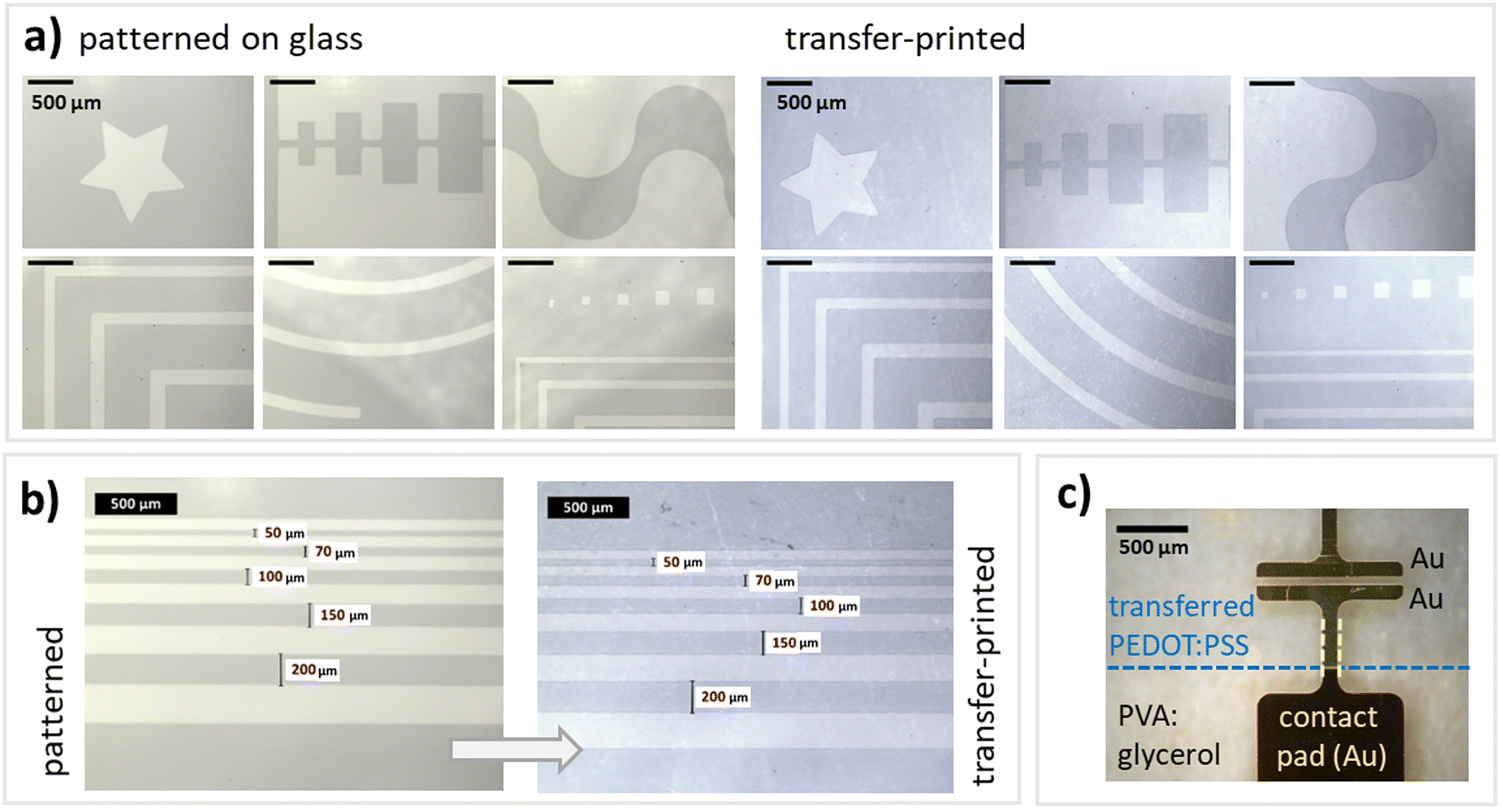 | ||
| Fig. 3 (a) Selection of microscope images of the O2-patterned PEDOT:PSS thin films on glass (left) and transfer-printed on to PVA:glycerol (25 wt%) substrates (right). (b) Patterned and transfer-printed stripes (minimal width: 50 μm). (c) Patterned PEDOT:PSS on PVA:glycerol substrates with top gold contacts (thermally evaporated in vacuum) for device applications. The length of each scale bar is 500 μm. | ||
Conclusions
In conclusion, a novel transfer-printing method for (plasma-patterned) PEDOT:PSS thin films was established which will highly benefit the processing of future flexible and stretchable electronics. Using this method, various (harsh) conductivity-enhancing treatments may be performed prior to transfer and hence without damaging the target substrate. Furthermore, the method relies on neither pre- nor post-treatments and allows the transfer of various film thicknesses and of large areas of film as well as various patterned structures. The electrical properties of the films are not impacted by this process. Lastly, the PVA substrates are water-soluble and allow for environmentally friendly disposal.Experimental
Materials
All materials (iso-propanol (IPA), acetone, DMSO, MeSO3H, H2SO4, EG, BSA, PVA, glycerol) were acquired from Sigma Aldrich, TCI, honeywell riedel-de haën, and PanReac AppliChem and used as received, without any further purification. PEDOT:PSS (Clevios PH1000 and AI4083, Hereaus Deutschland GmbH) was stored at 3.7 °C. Right before usage it was placed in an ultrasonic bath for 20 min and filtered through a 45 μm syringe filter.Transfer-printing of PEDOT:PSS thin films
All samples were prepared and measured in a clean room (temperature: 22 °C; humidity: 40–44%). First, glass carriers (7.5 cm × 2.5 cm) were cleaned in an ultrasonic bath in DI water for 5 min, acetone for 10 min and lastly IPA for 10 min. Afterwards, they were dried in an oven at 140 °C for 10 min. PVA:glycerol mixtures were prepared in DI water and stirred at 90 °C for three hours. 1 g PVA (Mw = 31![[thin space (1/6-em)]](https://www.rsc.org/images/entities/char_2009.gif) 000–50000 g mol−1, 99% hydrolyzed) was combined with 25 wt% glycerol in 9 mL DI water. Prior to usage the mixture was filtered through a 45 μm syringe filter and placed in an ultra sonic bath for 10 min. The mixture (1.5 mL) was drop-casted onto the previously cleaned glass slides and allowed to dry overnight yielding 95–100 μm thick films. To increase the wettability, the glass slides were previously exposed to a UV-ozone treatment for 20 min. PEDOT:PSS thin films were spin-coated on glass carriers at 500–1000 rpm for 60 s. Each treatment to increase the conductivity was performed following the respective procedure.2,12,37 The pristine PEDOT:PSS thin films were thermally annealed at 120 °C for 10 min after spin-coating. After peeling-off the PVA:glycerol substrates, they were carefully applied onto the PEDOT:PSS thin films and placed on a hot plate at 80 °C for 2 min (PVA:glycerol-side facing up). Transparencies were measured using an UV-vis spectrometer (Agilent Cary 60 UV-vis).
000–50000 g mol−1, 99% hydrolyzed) was combined with 25 wt% glycerol in 9 mL DI water. Prior to usage the mixture was filtered through a 45 μm syringe filter and placed in an ultra sonic bath for 10 min. The mixture (1.5 mL) was drop-casted onto the previously cleaned glass slides and allowed to dry overnight yielding 95–100 μm thick films. To increase the wettability, the glass slides were previously exposed to a UV-ozone treatment for 20 min. PEDOT:PSS thin films were spin-coated on glass carriers at 500–1000 rpm for 60 s. Each treatment to increase the conductivity was performed following the respective procedure.2,12,37 The pristine PEDOT:PSS thin films were thermally annealed at 120 °C for 10 min after spin-coating. After peeling-off the PVA:glycerol substrates, they were carefully applied onto the PEDOT:PSS thin films and placed on a hot plate at 80 °C for 2 min (PVA:glycerol-side facing up). Transparencies were measured using an UV-vis spectrometer (Agilent Cary 60 UV-vis).
Patterning of PEDOT:PSS thin films
A metal shadow mask was attached closely to the PEDOT:PSS thin film on glass, fixated using Kapton tape and then exposed to an O2-plasma for 4 min at 100 Watt and a process pressure of 50 Pa (Nordson AP-600 Plasma System). By ensuring that the mask is attached closely, only minor shadowing effects are observed. The patterned structures were then transfer-printed following the above described procedure. Gold contacts (300 nm) were evaporated in vacuum using a shadow mask.Electrical characterization
The conductivity was determined through I-V measurements using a two point probe set-up and a Keithley 2000 Multimeter. The film thickness was determined using a surface profilometer (Bruker, DektakXT Stylus Profiler). Depending on the treatment performed, film thicknesses ranged between 28 and 63 nm (see Table S2, ESI†).Imaging
PeakForce-Quantitative Nanomechanical Mapping (PF-QNM) SFM measurements were performed using a Bruker Dimension ICON platform using OLTESPA cantilevers (NanoAndMore GmbH, frequency: 70 kHz, spring constant: 2 Nm−1, back side coating: Al). From topography images, we calculated the root-mean-square roughness (rms also referred to as Image Rq) using the Nanoscope analysis software (Version 1.9). All rms- roughness values correspond to an area of 1 μm2. The mean adhesion force was determined for the same area. For all SFM-samples, PEDOT:PSS films were formed by spin-coated at 750 rpm for 60 s and the glyercol amount in the flexible substrates was 25 wt%. The samples were mounted to the SFM-wafer chuck using a double-sided tape. Optical microscope images were taken in bright field mode and edited using a confocal microscope (Leica DM6000 M) and the according software (Leica Application Suite Version 4.12.0).Conflicts of interest
There are no conflicts of interest to declare.Acknowledgements
This work was supported by the Max Planck Graduate Center with the Johannes Gutenberg-Universität Mainz (MPGC). U. K. and R. C. acknowledge funding from the VW foundation. We thank Helma Burg for supporting SFM measurements and Christian Bauer, Michelle Beuchel and Hanspeter Raich for their technical support. Open Access funding provided by the Max Planck Society.References
- O. Parlak, S. T. Keene, A. Marais, V. F. Curto and A. Salleo, Sci. Adv., 2018, 4, eaar2904 CrossRef CAS PubMed.
- X. Fan, B. Xu, S. Liu, C. Cui, J. Wang and F. Yan, ACS Appl. Mater. Interfaces, 2016, 8, 14029–14036 CrossRef CAS PubMed.
- J. Y. Oh, S. Rondeau-Gagné, Y. C. Chiu, A. Chortos, F. Lissel, G. J. N. Wang, B. C. Schroeder, T. Kurosawa, J. Lopez, T. Katsumata, J. Xu, C. Zhu, X. Gu, W. G. Bae, Y. Kim, L. Jin, J. W. Chung, J. B. H. Tok and Z. Bao, Nature, 2016, 539, 411–415 CrossRef CAS PubMed.
- W. Wang, S. Wang, R. Rastak, Y. Ochiai, S. Niu, Y. Jiang, P. K. Arunachala, Y. Zheng, J. Xu, N. Matsuhisa, X. Yan, S. K. Kwon, M. Miyakawa, Z. Zhang, R. Ning, A. M. Foudeh, Y. Yun, C. Linder, J. B. H. Tok and Z. Bao, Nat. Electron., 2021, 4, 143–150, DOI:10.1038/s41928-020-00525-1.
- Z. Zhang, W. Wang, Y. Jiang, Y. X. Wang, Y. Wu, J. C. Lai, S. Niu, C. Xu, C. C. Shih, C. Wang, H. Yan, L. Galuska, N. Prine, H. C. Wu, D. Zhong, G. Chen, N. Matsuhisa, Y. Zheng, Z. Yu, Y. Wang, R. Dauskardt, X. Gu, J. B. H. Tok and Z. Bao, Nature, 2022, 603, 624–630 CrossRef CAS PubMed.
- S. Zhang, Y. Li, G. Tomasello, M. Anthonisen, X. Li, M. Mazzeo, A. Genco, P. Grutter and F. Cicoira, Adv. Electron. Mater., 2019, 5, 1–7 Search PubMed.
- Y. Li, S. Zhang, X. Li, V. R. N. Unnava and F. Cicoira, Flex. Print. Electron., 2019, 4, 044004, DOI:10.1088/2058-8585/ab5202.
- D. Liu, X. Tian, J. Bai, Y. Wang, Y. Cheng, W. Ning, P. K. L. Chan, K. Wu, J. Sun and S. Zhang, Adv. Sci., 2022, 9, 1–7 CrossRef PubMed.
- X. Fan, W. Nie, H. Tsai, N. Wang, H. Huang, Y. Cheng, R. Wen, L. Ma, F. Yan and Y. Xia, Adv. Sci., 2019, 6, 1900813, DOI:10.1002/advs.201900813.
- H. Shi, C. Liu, Q. Jiang and J. Xu, Adv. Electron. Mater., 2015, 1, 1–16 Search PubMed.
- J. G. Troughton, B. Marchiori, R. Delattre, S. Escoubas, M. Y. Aliouat, S. Grigorian and M. Ramuz, Org. Electron., 2021, 92, 106108 CrossRef CAS.
- L. V. Lingstedt, M. Ghittorelli, H. Lu, D. A. Koutsouras, T. Marszalek, F. Torricelli, N. I. Crăciun, P. Gkoupidenis and P. W. M. Blom, Adv. Electron. Mater., 2019, 5, 1–8 Search PubMed.
- N. A. Shahrim, Z. Ahmad, A. Wong Azman, Y. Fachmi Buys and N. Sarifuddin, Mater. Adv., 2021, 2, 7118–7138 RSC.
- X. Fan, W. Song, T. Lei, B. Xu, F. Yan, N. Wang, H. Cui and Z. Ge, Mater. Chem. Front., 2019, 3, 901–908 RSC.
- U. Kraft, F. Molina-Lopez, D. Son, Z. Bao and B. Murmann, Adv. Electron. Mater., 2020, 6, 1900681, DOI:10.1002/aelm.201900681.
- Z. Rao, A. Thukral, P. Yang, Y. Lu, H. Shim, W. Wu, A. Karim and C. Yu, Adv. Funct. Mater., 2022, 32, 2111232, DOI:10.1002/adfm.202111232.
- N. Kim, H. Kang, J. H. Lee, S. Kee, S. H. Lee and K. Lee, Adv. Mater., 2015, 27, 2317–2323 CrossRef CAS PubMed.
- J. K. Kim, W. Kim, D. H. Wang, H. Lee, S. M. Cho, D. Choi and J. H. Park, Langmuir, 2013, 29, 5377–5382 CrossRef CAS PubMed.
- J. K. Kim, G. Veerappan, N. Heo, D. H. Wang and J. H. Park, J. Phys. Chem. C, 2014, 118, 22672–22677 CrossRef CAS.
- S. Zhang, H. Ling, Y. Chen, Q. Cui, J. Ni, X. Wang, M. C. Hartel, X. Meng, K. J. Lee, J. Lee, W. Sun, H. Lin, S. Emaminejad, S. Ahadian, N. Ashammakhi, M. R. Dokmeci and A. Khademhosseini, Adv. Funct. Mater., 2020, 30, 1906016, DOI:10.1002/adfm.201906016.
- S. Park, C. W. Lee and J. M. Kim, Org. Electron., 2018, 58, 1–5 CrossRef CAS.
- S. Chen, A. Surendran, X. Wu, S. Y. Lee, M. Stephen and W. L. Leong, Adv. Mater. Technol., 2020, 5, 1–23 Search PubMed.
- D. A. Koutsouras, F. Torricelli, P. Gkoupidenis and P. W. M. Blom, Adv. Mater. Technol., 2021, 6, 2100732, DOI:10.1002/admt.202100732.
- M. Zabihipour, R. Lassnig, J. Strandberg, M. Berggren, S. Fabiano, I. Engquist and P. Andersson Ersman, npj Flex. Electron., 2020, 4, 1–8 CrossRef.
- F. Molina-Lopez, T. Z. Gao, U. Kraft, C. Zhu, T. Öhlund, R. Pfattner, V. R. Feig, Y. Kim, S. Wang, Y. Yun and Z. Bao, Nat. Commun., 2019, 10, 1–10 CrossRef CAS PubMed.
- D. A. Koutsouras, F. Torricelli and P. W. M. Blom, Adv. Electron. Mater., 2023, 9, 2200868, DOI:10.1002/aelm.202200868.
- V. R. Feig, H. Tran, M. Lee, K. Liu, Z. Huang, L. Beker, D. G. Mackanic and Z. Bao, Adv. Mater., 2019, 31, 1–7 CrossRef PubMed.
- T. G. Kim, S. R. Ha, H. Choi, K. Uh, U. Kundapur, S. Park, C. W. Lee, S. H. Lee, J. Kim and J. M. Kim, ACS Appl. Mater. Interfaces, 2017, 9, 19231–19237 CrossRef CAS PubMed.
- Z. Zhu, G. Yang, R. Li and T. Pan, Microsyst. Nanoeng., 2017, 3, 1–9 Search PubMed.
- W. S. Chang, T. S. Chang, C. M. Wang and W. S. Liao, ACS Appl. Mater. Interfaces, 2022, 14, 22826–22837 CrossRef CAS PubMed.
- V. Kostianovskii, B. Sanyoto and Y. Y. Noh, Org. Electron., 2017, 44, 99–105 CrossRef CAS.
- H. Tian, L. Yuan, D. Zhou, J. Niu, H. Cong and A. Xiang, Polym. Adv. Technol., 2018, 29, 2612–2618 CrossRef CAS.
- H. Yuk, J. Wu and X. Zhao, Nat. Rev. Mater., 2022, 7, 935–952 CrossRef CAS.
- M. Mohsin, A. Hossin and Y. Haik, J. Appl. Polym. Sci., 2011, 112, 3102–3109 CrossRef.
- T. Liu, X. Peng, Y. N. Chen, Q. W. Bai, C. Shang, L. Zhang and H. Wang, Macromol. Rapid Commun., 2018, 39, 1–7 Search PubMed.
- E. Chiellini, A. Corti, S. D’Antone and R. Solaro, Prog. Polym. Sci., 2003, 28, 963–1014 CrossRef CAS.
- J. Rivnay, S. Inal, B. A. Collins, M. Sessolo, E. Stavrinidou, X. Strakosas, C. Tassone, D. M. Delongchamp and G. G. Malliaras, Nat. Commun., 2016, 7, 11287 CrossRef PubMed.
- X. Crispin, S. Marciniak, W. Osikowicz, G. Zotti, A. W. D. van der Gon, F. Louwet, M. Fahlman, L. Groenendaal, F. De Schryver and W. R. Salaneck, J. Polym. Sci., Part B: Polym. Phys., 2003, 41, 2561–2583 CrossRef CAS.
- A. M. Nardes, M. Kemerink, R. A. J. Janssen, J. A. M. Bastiaansen, N. M. M. Kiggen, B. M. W. Langeveld, A. J. J. M. Van Breemen and M. M. De Kok, Adv. Mater., 2007, 19, 1196–1200 CrossRef CAS.
- J. K. Kim, I. Park, W. Kim, D. H. Wang, D. G. Choi, Y. S. Choi and J. H. Park, ChemSusChem, 2014, 7, 1957–1963 CrossRef CAS PubMed.
- W. Meng, R. Ge, Z. Li, J. Tong, T. Liu, Q. Zhao, S. Xiong, F. Jiang, L. Mao and Y. Zhou, ACS Appl. Mater. Interfaces, 2015, 7, 14089–14094 CrossRef CAS PubMed.
- H. He, L. Zhang, S. Yue, S. Yu, J. Wei and J. Ouyang, Macromolecules, 2021, 54, 1234–1242 CrossRef CAS.
- T. Shimura, S. Sato, T. Tominaga, S. Abe, K. Yamashita, M. Ashizawa, T. Kato, H. Ishikuro and N. Matsuhisa, Adv. Mater. Technol., 2023, 8, 1–8 Search PubMed.
- K. Xu, W. Sun, Y. Shao, F. Wei, X. Zhang, W. Wang and P. Li, Nanotechnol. Rev., 2018, 7, 605–621 CrossRef CAS.
- Y. Y. Lee, J. H. Lee, J. Y. Cho, N. R. Kim, D. H. Nam, I. S. Choi, K. T. Nam and Y. C. Joo, Adv. Funct. Mater., 2013, 23, 4020–4027 CrossRef CAS.
- Y. Y. Lee, G. M. Choi, S. M. Lim, J. Y. Cho, I. S. Choi, K. T. Nam and Y. C. Joo, Sci. Rep., 2016, 6, 1–9 CrossRef PubMed.
- Y. Wang, C. Zhu, R. Pfattner, H. Yan, L. Jin, S. Chen, F. Molina-Lopez, F. Lissel, J. Liu, N. I. Rabiah, Z. Chen, J. W. Chung, C. Linder, M. F. Toney, B. Murmann and Z. Bao, Sci. Adv., 2017, 3, 1–10, DOI:10.1126/sciadv.1602076.
- E. Hosseini, V. Ozhukil Kollath and K. Karan, J. Mater. Chem. C, 2020, 8, 3982–3990 RSC.
- C. Wang, K. Sun, J. Fu, R. Chen, M. Li, Z. Zang, X. Liu, B. Li, H. Gong and J. Ouyang, Adv. Sustainable Syst., 2018, 2, 1–9 Search PubMed.
- Y. H. Kim, C. Sachse, M. L. MacHala, C. May, L. Müller-Meskamp and K. Leo, Adv. Funct. Mater., 2011, 21, 1076–1081 CrossRef CAS.
- W. Song, X. Fan, B. Xu, F. Yan, H. Cui, Q. Wei, R. Peng, L. Hong, J. Huang and Z. Ge, Adv. Mater., 2018, 30, 1800075, DOI:10.1002/adma.201800075.
- X. Wang, A. K. K. Kyaw, C. Yin, F. Wang, Q. Zhu, T. Tang, P. I. Yee and J. Xu, RSC Adv., 2018, 8, 18334–18340 RSC.
- D. Alemu Mengistie, P. C. Wang and C. W. Chu, J. Mater. Chem. A, 2013, 1, 9907–9915 RSC.
- U. Lang, E. Muller, N. Naujoks and J. Dual, Adv. Funct. Mater., 2009, 19, 1215–1220 CrossRef CAS.
- N. Kim, S. Kee, S. H. Lee, B. H. Lee, Y. H. Kahng, Y. R. Jo, B. J. Kim and K. Lee, Adv. Mater., 2014, 26, 2268–2272 CrossRef CAS PubMed.
Footnote |
| † Electronic supplementary information (ESI) available: [DETAILS]. See DOI: https://doi.org/10.1039/d3tc04485h |
| This journal is © The Royal Society of Chemistry 2024 |