
Low-temperature vapor reduction of graphene oxide electrodes for vertical organic field-effect transistors†
Kun
Qiao
 ,
Qing
Ma
,
Junjia
Wang
and
Binghao
Wang
*
,
Qing
Ma
,
Junjia
Wang
and
Binghao
Wang
*
School of Electronic Science & Engineering, Southeast University, 2 Sipailou Road, Nanjing, Jiangsu Province 210096, P. R. China. E-mail: binghaowang@seu.edu.cn
First published on 30th November 2023
Abstract
Graphene based vertical organic field-effect transistors (VOFETs) are promising devices for realizing a high current density at a low operation voltage. However, high-quality graphene typically requires a high temperature and a complicated fabrication process, presenting a major barrier to roll-to-roll manufacturing. Here, we report a low temperature (⩽45 °C), vapor (HI)-assisted process to achieve ultrathin and uniform reduced graphene oxide (rGO) films with a higher electrical conductivity compared with conventional high-temperature reduction methods. Notably, VOFETs with rGO source electrodes exhibited the highest current on/off ratio exceeding 104 and a maximum current density of 14.4 mA cm−2 owing to the gate-tunable work function characteristics of the prepared rGO. The current density of the device could be further improved by increasing the conductivity of the rGO electrode with additional thermal treatment. The synergy of low-temperature and HI vapor endowed rGO-VOFET devices with excellent current density, on/off ratio, and gate-tunable ability, making them promising candidates for future flexible organic electronics.
 Binghao Wang | Binghao Wang is a Professor of Electronic Science and Technology at Southeast University. Prior to this, he was a Project Researcher at The University of Tokyo, and a Joint-PhD student and Postdoctoral Researcher at Northwestern University. He obtained his B.E., M.S., and PhD degrees from Soochow University. His research interests encompass flexible/wearable thin-film transistors and sensors, with a portfolio that includes over 80 co-authored papers and contributions to 2 book chapters. |
Introduction
The ultrashort channel length of the vertical organic field-effect transistors (VOFETs) enables the fabrication of devices in a smaller size with improved electrical performance compared with their lateral counterparts.1–4 So far, various VOFETs based on graphene electrodes have been reported due to their excellent conductivity in a two-dimensional form.5–14 In these devices, the work function tunability of graphene is exploited via an external gate electrical field to modulate the injection barrier height at the graphene/organic semiconductor interface.5–7 However, almost all these devices utilized single-layer graphene obtained by the capital-intensive chemical vapor deposition (CVD) method. Although the CVD method can produce high-quality graphene, the rather complicated transfer process of graphene to the substrate is incompatible with future large-scale roll-to-roll applications.Reduced graphene oxide (rGO) has a similar structure and properties to graphene.15–19 Most importantly, it can be easily mass-produced via reduction of low-cost solution-processable graphene oxide (GO). To achieve high-performance devices, the rGO film should possess not only high electrical conductivity, but also ultrathin and uniform film morphology. Although high temperature (>800 °C) thermal reduction could prepare rGO films with high electrical conductivity, the involved high temperature is not applicable to emerging flexible electronics.20–23 In this regard, chemical reduction is preferred because of its low reduction temperature.24–28 In particular, chemical reduction by the vapor phase is more promising because dipping the substrate with the GO film in a hot reducing solution would inevitably ruin and even peel off the rGO film from the substrate,20,29 which would greatly degrade the device performance. The rGO films prepared by vapor phase reduction, such as with hydrazine vapor, normally suffer from poor electrical conductivity, and further thermal reduction treatment (>300 °C) is usually required to improve their electrical properties.20,30 Therefore, using low-temperature vapor phase reduction to prepare rGO films with good electrical conductivity is highly desirable.
Another critical requirement for using rGO electrodes in VOFETs is ultrathin thickness. The operation of this type of VOFET is based on the gate-tunable work function mechanism,31 whereas the work-function tuning induced by the gate electrical field only occurs in an ultrathin rGO film.32,33 In addition, the ultrathin rGO electrode benefits the partial screening effect of the gate electrical field,4,11 which could further improve the device performance. In a previous work, a simple spin-coating and reduction method was proposed that can effectively prepare highly conductive and ultrathin rGO films.34 By employing hydrazine monohydrate vapor reduction along with 300 °C treatment for 6 h, we achieved a conductivity of 10 S cm−1 for the rGO film and a current density of 0.73 mA cm−2 for VOFETs. However, it involved high temperature long-term thermal annealing, making it difficult for flexible devices.
In this study, we report a low-temperature (⩽45 °C) HI vapor reduction of ultrathin GO films and used them as electrodes for VOFETs. Despite such mild reduction conditions, the resulting rGO film exhibits a sheet resistance of 0.56 MΩ sq−1, which is better than those (1.1 MΩ sq−1) reduced by 300 °C annealing for 6 h. X-ray photoelectron spectroscopy (XPS) also demonstrates a higher reduction level by the HI vapor than thermal treatment. By sandwiching organic semiconductor N,N′-dioctyl-3,4,9,10-perylenedicarboximide (PTCDI-C8) between the rGO and an Al electrode on an n++Si/SiO2 substrate, the fabricated device (rGO-VOFET) generated the highest current on/off ratio of over 104 and a maximum current density of 14.4 mA cm−2.
Results and discussion
A schematic of the device fabrication process is illustrated in Fig. S1 (ESI†). An ultrathin GO film was first formed on an n++Si/SiO2 substrate by spin-coating a purified GO dispersion. The substrate was placed in a sealed container with HI solution, and the GO film was reduced by exposure to HI vapor. Notably, the reduction temperature was less than 45 °C. After wet-patterning of the rGO film, a 350 nm-thick PTCDI-C8 layer and 50 nm-thick Al electrode were sequentially deposited through shadow masks using a vacuum thermal evaporator, and the final device rGO-VOFETs were fabricated. The top-view optical image and three-dimensional schematic of the device are shown in Fig. 1a and b, respectively. The active area of the device determined by the overlapping area of the top drain and bottom rGO electrode was 200 × 100 μm2.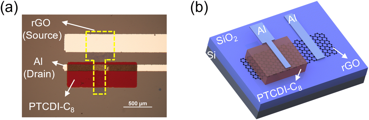 | ||
| Fig. 1 (a) Top-view optical image and (b) three-dimensional schematic of the device. | ||
Ultrathin and uniform films with high coverage are required for the gate-tunable work function electrode.31 The morphology of the GO and rGO films were first evaluated by optical microscopy. As shown in Fig. 2a, the spin-coated GO film on the n++Si/SiO2 substrate shows a semi-transparent feature and high coverage. After HI vapor reduction, the rGO film (Fig. 2b) on the n++Si/SiO2 substrate exhibits better contrast due to the improved reflection of incident light.35 This large-scale high coverage of the rGO film is further demonstrated in Fig. S2 (ESI†). The surface morphology of the GO and rGO films is evaluated by atomic force microscopy (AFM). Fig. 2c shows the spin-coated GO film before reduction, where ultrathin GO flakes uniformly cover the surface. The thickness of the GO film is about 1 nm (Fig. S3, ESI†), indicating its monolayer structure.26 Importantly, this ultrathin and high-coverage film is maintained after reduction by exposure to HI vapor (Fig. 2d). In contrast, the surface of the rGO film reduced by dipping in HI solution is uneven and contaminated (Fig. S4, ESI†). The results reveal that vapor phase reduction is necessary to keep a clean and smooth surface of the rGO film.
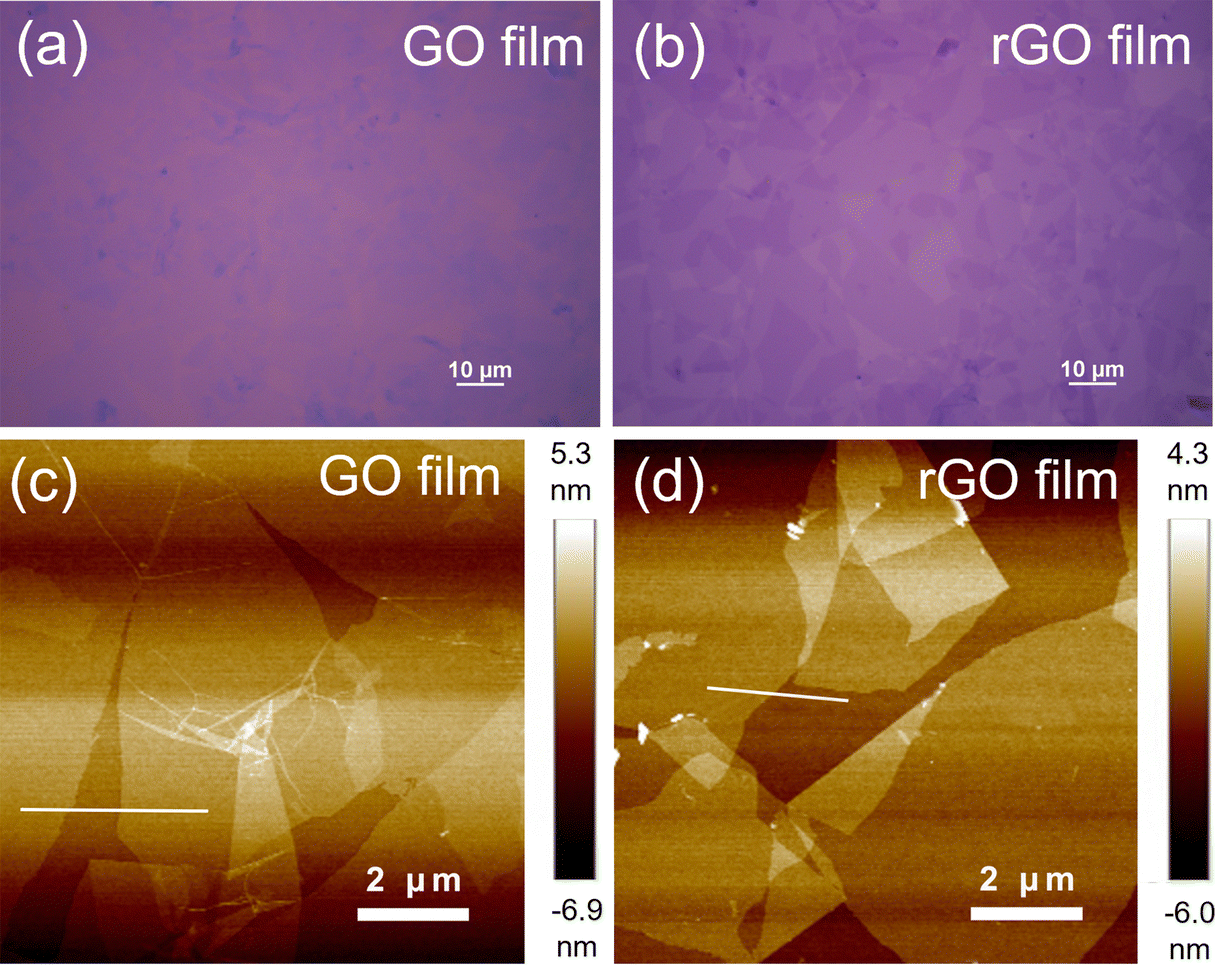 | ||
| Fig. 2 Optical images of the (a) GO and (b) rGO films. AFM images of the (c) GO and (d) rGO films. | ||
The electrical conductivities of the rGO films are evaluated by measuring their sheet resistance (Rs) via a four-probe method, as it plays a critical role in device performance. For the low-temperature HI vapor reduction method, the impact of the reduction temperature and reduction time on the Rs are systematically investigated. First, the GO films are reduced by exposure to HI vapor at 30, 45, and 60 °C for 12 h, respectively. As shown in Fig. 3a, the Rs of the rGO film dramatically decreases from 0.94 to 0.56 MΩ sq−1 as the reduction temperature increases from 30 to 45 °C. Further increasing the reduction temperature to 60 °C does not reduce the Rs too much, suggesting that HI vapor treatment at 45 °C is enough to reduce the GO film. Next, the Rs of the rGO film is further evaluated by exposure of the GO film to HI vapor at 45 °C for 6, 12, 18, and 24 h, respectively (Fig. 3b). The Rs decreases slowly as the time increases, especially for that treated for more than 12 h. Thus, HI vapor treatment at 45 °C for 12 h was chosen as the optimal condition (rGO-HI). Moreover, we compare the Rs of the rGO films prepared by other methods (Fig. 3c). The rGO films were prepared by direct thermal annealing at 300 °C for 6 h (rGO-300 °C), and post annealing of rGO-HI at 300 °C for 1 h (rGO-HI-300 °C), respectively. Compared with the rGO-300 °C film, the electrical conductivity of the rGO-HI is significantly improved, indicating that this low-temperature HI vapor reduction method is more effective to reduce the rGO film. Moreover, by post annealing at 300 °C for 1 h, the electrical conductivity of the rGO-HI-300 °C film could be further improved.
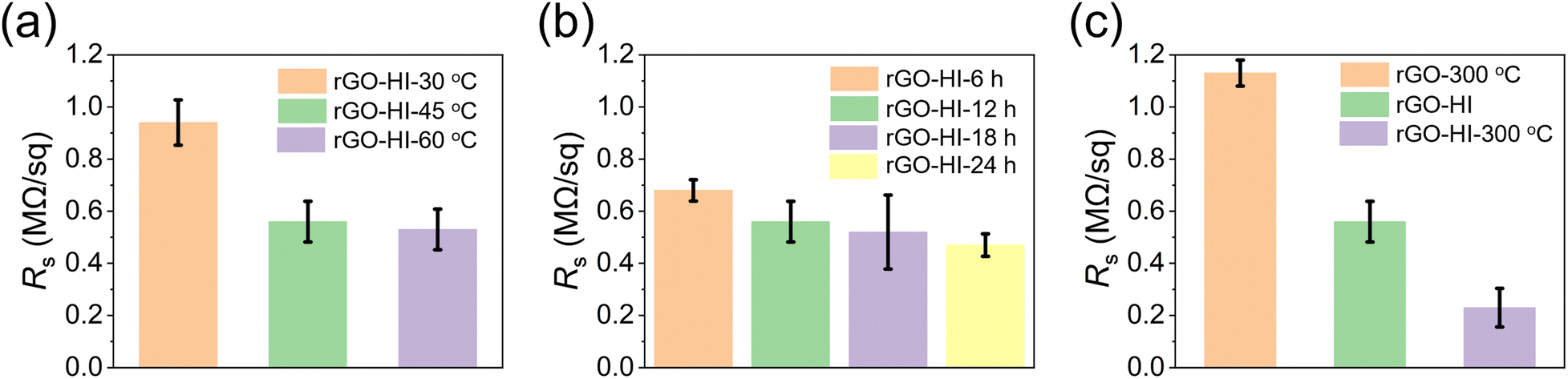 | ||
| Fig. 3 (a) Rs of the rGO films reduced by HI vapor at 30, 45 and 60 °C for 12 h, respectively. (b) Rs of the rGO films reduced by HI vapor at 45 °C for 6, 12, 18, and 24 h, respectively. (c) Rs of the rGO-300 °C, rGO-HI, and rGO-HI-300 °C films, respectively. | ||
To precisely reveal the reduction extent of the rGO films by these different methods, XPS analysis is performed. As shown in Fig. S5 (ESI†), the C1s XPS spectrum of the GO film can be divided into three peaks at around 288.1, 286.5, and 284.2 eV, arising from the C![[double bond, length as m-dash]](https://www.rsc.org/images/entities/char_e001.gif) O, C–O, and C–C bonds, respectively.25,26 The CO and C–O bonds account for oxygen-containing groups in the GO film. After reduction treatment, the intensities of the corresponding CO and C–O peaks dramatically decrease, while the C–C peak becomes the dominant peak. Notably, compared with the C1s XPS spectrum of rGO-300 °C, the intensities of the C–O and CO peaks of the rGO-HI film are much weaker, indicating a higher reduction level of the HI vapor-prepared rGO film. In addition, the reduction level of the rGO-HI film could be further improved by post annealing at 300 °C for 1 h. The corresponding CO, C–O, and C–C peak intensities of these rGO films are summarized in Fig. 4. The XPS analysis consists of conductivity tests. Raman spectra are further investigated to study these rGO films (Fig. S6, ESI†). Two prominent peaks at 1353 and 1587 cm−1 in the Raman spectra correspond to typical D and G peaks, respectively. Compared with rGO-300 °C, the increased ID/IG ratios of rGO-HI and rGO-HI-300 °C indicate the increase of the sp2 domain with decreased size,25,26 contributing to higher electrical conductivity.
O, C–O, and C–C bonds, respectively.25,26 The CO and C–O bonds account for oxygen-containing groups in the GO film. After reduction treatment, the intensities of the corresponding CO and C–O peaks dramatically decrease, while the C–C peak becomes the dominant peak. Notably, compared with the C1s XPS spectrum of rGO-300 °C, the intensities of the C–O and CO peaks of the rGO-HI film are much weaker, indicating a higher reduction level of the HI vapor-prepared rGO film. In addition, the reduction level of the rGO-HI film could be further improved by post annealing at 300 °C for 1 h. The corresponding CO, C–O, and C–C peak intensities of these rGO films are summarized in Fig. 4. The XPS analysis consists of conductivity tests. Raman spectra are further investigated to study these rGO films (Fig. S6, ESI†). Two prominent peaks at 1353 and 1587 cm−1 in the Raman spectra correspond to typical D and G peaks, respectively. Compared with rGO-300 °C, the increased ID/IG ratios of rGO-HI and rGO-HI-300 °C indicate the increase of the sp2 domain with decreased size,25,26 contributing to higher electrical conductivity.
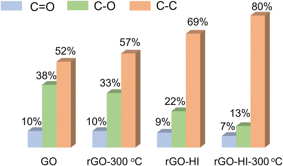 | ||
| Fig. 4 The intensity ratios of CO, C–O, and C–C peaks, obtained from the C1s XPS spectra of GO, rGO-300 °C, rGO-HI, and rGO-HI-300 °C, respectively. | ||
The electrical conductivity of rGO relies on the recovery of its conjugated structure by eliminating these oxygen-containing groups (epoxy, hydroxyl, and carbonyl groups). For rGO-300 °C, the reduction level of the rGO film mainly depends on the reduction temperature. However, the temperature of 300 °C is not high enough to considerably eliminate these oxygen functional groups.17,35 For the rGO-HI film, the reduction is through the substitution of oxygen functional groups by iodine atoms.29,36 Owing to the strong HI acid and weak C–I bond, the oxygen functional groups in the GO film can be effectively removed at a much lower temperature.36
Furthermore, VOFETs were fabricated based on the rGO-300 °C, rGO-HI, and rGO-HI-300 °C films. The electrical properties of the devices are estimated at room temperature under dark conditions. The rGO source electrodes are grounded, whereas the top Al drain electrodes and bottom gate electrodes are biased with respect to the ground. In the output characteristics (Fig. 5a–c), a larger drain current (IDS) is observed with a more positive gate voltage (VGS), indicating that they are typical n-type transistors. Notably, the highest IDS values of the devices gradually rise with the increasing electrical conductivity of the rGO electrodes. The transfer characteristics of the devices (Fig. 5d–f) are measured at the drain voltage (VDS) of +30 V. As shown in Fig. 5d, the device based on the rGO-300 °C film shows a relatively low current on/off ratio (∼100) with large hysteresis, which could be attributed to the presence of the traps at the rGO/PTCDI-C8 interface. As discussed before, 300 °C thermal treatment is not enough to reduce the GO film; therefore, there should be many oxygen functional groups remaining in the rGO-300 °C film, resulting in poor device performance. By contrast, the electrical properties of the device based on the rGO-HI film are significantly improved (Fig. 5e), exhibiting the highest current on/off ratio exceeding 104 and a maximum current density of 14.4 mA cm−2 with small hysteresis. The performance is comparable to those of VOFETs based on CVD-grown graphene electrodes.5,12Fig. 5f illustrates the transfer characteristics of the device based on the rGO-HI-300 °C film. Due to the improved electrical conductivity of the rGO electrode, the highest current density of the device is further improved to 21.9 mA cm−2.
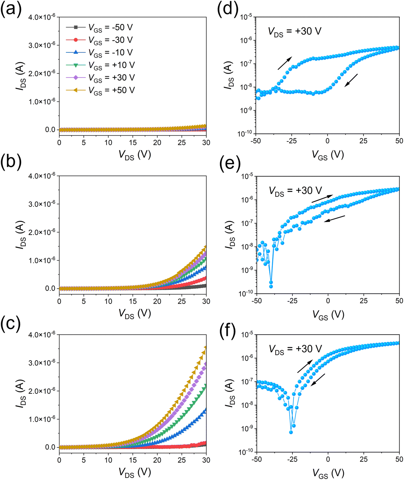 | ||
| Fig. 5 (a)–(c) Output characteristics and (d)–(f) transfer characteristics of rGO-300 °C, rGO-HI, and rGO-HI-300 °C, respectively. | ||
Conclusions
In this work, VOFETs based on a low temperature-prepared rGO electrode were fabricated, achieving a large current density and a high on/off ratio. An ultrathin GO film with high coverage is first prepared by spin-coating a highly purified GO dispersion. Then, low-temperature HI vapor is utilized to reduce the spin-coated GO film to maintain the highly covered film structure and enable its application to future flexible devices. By using these mild reaction conditions, the prepared rGO film possesses very low sheet resistance of 0.56 MΩ sq−1 and gate-tunable work function characteristics. The assembled rGO-VOFET devices exhibit satisfactory performance with the highest current on/off ratio of over 104 and a maximum current density of 14.4 mA cm−2. Moreover, the current density of the device is closely related to the conductivity of the rGO electrode and could be further improved. Importantly, we anticipate that this low-temperature HI vapor-prepared rGO electrode will help in advancing low-cost, high-performance, roll-to-roll future flexible organic electronics.Experimental section
Purification of the GO dispersion
The commercial GO dispersion (4 mg mL−1, GaoxiTech Corp, China) was firstly purified by a series of centrifugation treatments. The details of the centrifugation process are as follows: the GO dispersion was first diluted to 1 mg mL−1, the solution was centrifuged at 3800 rpm for 15 min to remove the precipitate. Then, the supernatant liquid was centrifuged at 2300 rpm for 30 min to further remove the precipitate. This process was repeated 4 times. After that, the supernatant liquid was centrifugated at 4000 rpm for 1 h to collect the precipitate. After drying, the precipitate was diluted to 1 mg mL−1 for further use.Device fabrication process
The fabrication process of the rGO-VOFETs is as follows: the purified GO dispersion (300 μL) was dripped onto n++Si/SiO2 substrates (300 nm-thick), followed by spin-coating at 500 rpm/120 s, 1000 rpm/30 s and 2000 rpm/30 s sequentially to prepare the ultrathin GO film. Then, the spin-coated GO film was placed in a 250 mL sealed container with 3 mL HI solution (55–57%, Adamas, China), and the container was kept at different temperatures for different times. After the reduction treatment, the rGO film was patterned by a wet patterning method.37 Briefly, 100 nm-thick Au was deposited through a shadow mask on the rGO film as a protective layer. Then, the substrate was placed in a beaker filled with bleaching solution (Kaneyo Corp, Japan) under UV light (365 nm, 3 W cm−2) irradiation directed on the substrate. After 2 min irradiation, the substrate was carefully rinsed with deionized water and dried by condensed air flow. Then the Au was removed by dipping in KI/I2 solution for around 1 min. The substrate was rinsed with deionized water to remove the residual KI/I2 solution and then dried by condensed air flow. KI/I2 solution was prepared by dissolving 1.6 g KI powder (99%, Adamas, China) and 0.4 g I2 (99%, Adamas, China) in 50 mL deionized water. Subsequently, 350 nm-thick n-type organic semiconductor PTCDI-C8 (Luminescence Technology Corp., China) was deposited as an organic layer at a rate of 3 Å s−1 through a shadow mask using a vacuum thermal evaporator. The vacuum chamber pressure was under 3 × 10⁻⁶ torr. Finally, a 50 nm-thick Al electrode was thermally deposited at a rate of 2 Å s−1 under a vacuum pressure of 6 × 10⁻⁶ torr to fabricate the rGO-VOFET devices. The active area of the device determined by the overlapping area of the bottom rGO and top Al drain electrode is 200 × 100 μm2.Measurements and characterizations
The electrical properties of the devices were measured using a semiconductor parameter analyzer (Keithley 4200-SCS, US) at room temperature under dark conditions. The Rs of the rGO film was evaluated by using four-probe equipment (JG ST2258C, Suzhou Jingge Electronic Corp., China). The surface morphology of the GO and rGO films was investigated by using a Bruker Dimensional Icon atomic force microscopy system in tapping mode. XPS was performed on a JEOL JPS-9010MC spectrometer and O(1s) spectra were fitted using three Gaussian−Lorentzian convolution functions after subtracting a linear baseline.Conflicts of interest
The authors declare no competing financial interest.Acknowledgements
This work is supported by the National Natural Science Foundation of China (Grant No. 22305036), the Natural Science Foundation of Jiangsu Province (Grant No. BK20220815), the Fundamental Research Funds for the Central Universities (Grant No. 4006002302), and the Program of Jiangsu Specially-Appointed Professor. Dr Ma acknowledges the support from the Jiangsu Funding Program for Excellent Postdoctoral Talent (Award No. 2022ZB85). The authors also thank Dr Qichao Chen for the sheet resistance test and Dr. Di Xue (Soochow University) for the AFM test.Notes and references
- D. Dahal, P. R. Paudel, V. Kaphle, R. K. Radha Krishnan and B. Lüssem, Influence of Injection Barrier on Vertical Organic Field Effect Transistors, ACS Appl. Mater. Interfaces, 2022, 14, 7063–7072, DOI:10.1021/acsami.1c20382.
- Y. Chen, Y. Yao, N. Turetta and P. Samorì, Vertical Organic Transistors with Short Channels for Multifunctional Optoelectronic Devices, J. Mater. Chem. C, 2022, 10, 2494–2506, 10.1039/D1TC05055A.
- J. Liu, Z. Qin, H. Gao, H. Dong, J. Zhu and W. Hu, Vertical Organic Field-Effect Transistors, Adv. Funct. Mater., 2019, 29, 1808453, DOI:10.1002/adfm.201808453.
- S. Parui, M. Ribeiro, A. Atxabal, R. Llopis, F. Casanova and L. E. Hueso, Graphene as an Electrode for Solution-Processed Electron-Transporting Organic Transistors, Nanoscale, 2017, 9, 10178–10185, 10.1039/C7NR01007A.
- J. S. Kim, B. J. Kim, Y. J. Choi, M. H. Lee, M. S. Kang and J. H. Cho, An Organic Vertical Field-Effect Transistor with Underside-Doped Graphene Electrodes, Adv. Mater., 2016, 28, 4803–4810, DOI:10.1002/adma.201505378.
- M. G. Lemaitre, E. P. Donoghue, M. A. McCarthy, B. Liu, S. Tongay, B. Gila, P. Kumar, R. K. Singh, B. R. Appleton and A. G. Rinzler, Improved Transfer of Graphene for Gated Schottky-Junction, Vertical, Organic, Field-Effect Transistors, ACS Nano, 2012, 6, 9095–9102, DOI:10.1021/nn303848k.
- S. Parui, L. Pietrobon, D. Ciudad, S. Vélez, X. Sun, F. Casanova, P. Stoliar and L. E. Hueso, Gate-Controlled Energy Barrier at a Graphene/Molecular Semiconductor Junction, Adv. Funct. Mater., 2015, 25, 2972–2979, DOI:10.1002/adfm.201403407.
- Y. Liu, H. Zhou, N. O. Weiss, Y. Huang and X. Duan, High-Performance Organic Vertical Thin Film Transistor Using Graphene as a Tunable Contact, ACS Nano, 2015, 9, 11102–11108, DOI:10.1021/acsnano.5b04612.
- J. Liu, K. Zhou, J. Liu, J. Zhu, Y. Zhen, H. Dong and W. Hu, Organic-Single-Crystal Vertical Field-Effect Transistors and Phototransistors, Adv. Mater., 2018, 30, 1803655, DOI:10.1002/adma.201803655.
- B. Sun, C.-H. Zhu, Y. Liu, C. Wang, L.-J. Wan and D. Wang, Oriented Covalent Organic Framework Film on Graphene for Robust Ambipolar Vertical Organic Field-Effect Transistor, Chem. Mater., 2017, 29, 4367–4374, DOI:10.1021/acs.chemmater.7b00800.
- C.-J. Shih, R. Pfattner, Y.-C. Chiu, N. Liu, T. Lei, D. Kong, Y. Kim, H.-H. Chou, W.-G. Bae and Z. Bao, Partially-Screened Field Effect and Selective Carrier Injection at Organic Semiconductor/Graphene Heterointerface, Nano Lett., 2015, 15, 7587–7595, DOI:10.1021/acs.nanolett.5b03378.
- D. U. Lim, S. Kim, Y. J. Choi, S. B. Jo and J. H. Cho, Percolation-Limited Dual Charge Transport in Vertical p – n Heterojunction Schottky Barrier Transistors, Nano Lett., 2020, 20, 3585–3592, DOI:10.1021/acs.nanolett.0c00523.
- J. S. Kim, Y. J. Choi, H. J. Woo, J. Yang, Y. J. Song, M. S. Kang and J. H. Cho, Schottky-Barrier-Controllable Graphene Electrode to Boost Rectification in Organic Vertical P-N Junction Photodiodes, Adv. Funct. Mater., 2017, 27, 1704475, DOI:10.1002/adfm.201704475.
- H. Hlaing, C.-H. Kim, F. Carta, C.-Y. Nam, R. A. Barton, N. Petrone, J. Hone and I. Kymissis, Low-Voltage Organic Electronics Based on a Gate-Tunable Injection Barrier in Vertical Graphene-Organic Semiconductor Heterostructures, Nano Lett., 2015, 15, 69–74, DOI:10.1021/nl5029599.
- R. Tarcan, O. Todor-Boer, I. Petrovai, C. Leordean, S. Astilean and I. Botiz, Reduced Graphene Oxide Today, J. Mater. Chem. C, 2020, 8, 1198–1224, 10.1039/C9TC04916A.
- M. Sedki, P. S. Mirabedini, K. Nakama, G. Stephens, M. Groves, I. Lee, M. R. Neupane and A. Mulchandani, Synthesis of Pristine Graphene-like Behaving RGO Thin Film: Insights into What Really Matters, Carbon, 2022, 186, 437–451, DOI:10.1016/j.carbon.2021.10.011.
- V. Agarwal and P. B. Zetterlund, Strategies for Reduction of Graphene Oxide – A Comprehensive Review, Chem. Eng. J., 2021, 405, 127018, DOI:10.1016/j.cej.2020.127018.
- A. Razaq, F. Bibi, X. Zheng, R. Papadakis, S. H. M. Jafri and H. Li, Review on Graphene-, Graphene Oxide-, Reduced Graphene Oxide-Based Flexible Composites: From Fabrication to Applications, Materials, 2022, 15, 1012, DOI:10.3390/ma15031012.
- Z. Zhao, P. Bai, W. Du, B. Liu, D. Pan, R. Das, C. Liu and Z. Guo, An Overview of Graphene and Its Derivatives Reinforced Metal Matrix Composites: Preparation, Properties and Applications, Carbon, 2020, 170, 302–326, DOI:10.1016/j.carbon.2020.08.040.
- H. A. Becerril, J. Mao, Z. Liu, R. M. Stoltenberg, Z. Bao and Y. Chen, Evaluation of Solution-Processed Reduced Graphene Oxide Films as Transparent Conductors, ACS Nano, 2008, 2, 463–470, DOI:10.1021/nn700375n.
- S. Wang, P. K. Ang, Z. Wang, A. L. L. Tang, J. T. L. Thong and K. P. Loh, High Mobility, Printable, and Solution-Processed Graphene Electronics, Nano Lett., 2010, 10, 92–98, DOI:10.1021/nl9028736.
- J. D. Renteria, S. Ramirez, H. Malekpour, B. Alonso, A. Centeno, A. Zurutuza, A. I. Cocemasov, D. L. Nika and A. A. Balandin, Strongly Anisotropic Thermal Conductivity of Free-Standing Reduced Graphene Oxide Films Annealed at High Temperature, Adv. Funct. Mater., 2015, 25, 4664–4672, DOI:10.1002/adfm.201501429.
- S.-Y. Kim, H.-E. Gang, G.-T. Park, H.-B. Jeon and Y. G. Jeong, Microstructure and Electrothermal Characterization of Transparent Reduced Graphene Oxide Thin Films Manufactured by Spin-Coating and Thermal Reduction, Results Phys., 2021, 24, 104107, DOI:10.1016/j.rinp.2021.104107.
- B. Kariminejad, M. Salami-Kalajahi, H. Roghani-Mamaqani and A. Noparvar-Qarebagh, Effect of Surface Chemistry of Graphene and Its Content on the Properties of Ethylene Dichloride- and Disodium Tetrasulfide-Based Polysulfide Polymer Nanocomposites, Polym. Compos., 2017, 38, E515–E524, DOI:10.1002/pc.23857.
- Z. Hou, Y. Zhou, G. Li, S. Wang, M. Wang, X. Hu and S. Li, Reduction of Graphene Oxide and Its Effect on Square Resistance of Graphene Films, Bull. Korean Chem. Soc., 2015, 36, 1681–1687, DOI:10.1002/bkcs.10323.
- Y. Shen, S. Yang, P. Zhou, Q. Sun, P. Wang, L. Wan, J. Li, L. Chen, X. Wang, S. Ding and D. W. Zhang, Evolution of the Band-Gap and Optical Properties of Graphene Oxide with Controllable Reduction Level, Carbon, 2013, 62, 157–164, DOI:10.1016/j.carbon.2013.06.007.
- A. C. Reynosa-Martínez, E. Gómez-Chayres, R. Villaurrutia and E. López-Honorato, Controlled Reduction of Graphene Oxide Using Sulfuric Acid, Materials, 2020, 14, 59, DOI:10.3390/ma14010059.
- J. Guo, B. Mao, J. Li, X. Wang and X. Yang, Rethinking the Reaction Pathways of Chemical Reduction of Graphene Oxide, Carbon, 2021, 171, 963–967, DOI:10.1016/j.carbon.2020.09.049.
- I. K. Moon, J. Lee, R. S. Ruoff and H. Lee, Reduced Graphene Oxide by Chemical Graphitization, Nat. Commun., 2010, 1, 73, DOI:10.1038/ncomms1067.
- J. O. Hwang, J. S. Park, D. S. Choi, J. Y. Kim, S. H. Lee, K. E. Lee, Y.-H. Kim, M. H. Song, S. Yoo and S. O. Kim, Workfunction-Tunable, N-Doped Reduced Graphene Transparent Electrodes for High-Performance Polymer Light-Emitting Diodes, ACS Nano, 2012, 6, 159–167, DOI:10.1021/nn203176u.
- Y. J. Choi, J. S. Kim, J. Y. Cho, H. J. Woo, J. Yang, Y. J. Song, M. S. Kang, J. T. Han and J. H. Cho, Tunable Charge Injection via Solution-Processed Reduced Graphene Oxide Electrode for Vertical Schottky Barrier Transistors, Chem. Mater., 2018, 30, 636–643, DOI:10.1021/acs.chemmater.7b03460.
- A. Geim and K. Novoselov, The rise of graphene, Nat. Mater, 2007, 6, 183–191, DOI:10.1038/nmat1849.
- A. A. Avetisyan, B. Partoens and F. M. Peeters, Electric-Field Control of the Band Gap and Fermi Energy in Graphene Multilayers by Top and Back Gates, Phys. Rev. B: Condens. Matter Mater. Phys., 2009, 80, 195401, DOI:10.1103/PhysRevB.80.195401.
- K. Qiao, S. Arakaki, M. Suzuki and K. Nakayama, Performance Improvement with an Ultrathin p-Type Interfacial Layer in n-Type Vertical Organic Field-Effect Transistors Based on Reduced Graphene Oxide Electrode, ACS Omega, 2022, 7, 24468–24474, DOI:10.1021/acsomega.2c02085.
- S. Pei and H.-M. Cheng, The Reduction of Graphene Oxide, Carbon, 2012, 50, 3210–3228, DOI:10.1016/j.carbon.2011.11.010.
- S. Pei, J. Zhao, J. Du, W. Ren and H.-M. Cheng, Direct Reduction of Graphene Oxide Films into Highly Conductive and Flexible Graphene Films by Hydrohalic Acids, Carbon, 2010, 48, 4466–4474, DOI:10.1016/j.carbon.2010.08.006.
- M. Zhang, M. Yang, Y. Okigawa, T. Yamada, H. Nakajima, Y. Iizumi and T. Okazaki, Patterning of Graphene Using Wet Etching with Hypochlorite and UV Light, Sci. Rep., 2022, 12(1), 4541, DOI:10.1038/s41598-022-08674-3.
Footnote |
| † Electronic supplementary information (ESI) available: Fabrication process of the device, optical images of rGO films, a height profile of the GO film, AFM images of the rGO films, and XPS spectra and Raman spectra of the rGO films. See DOI: https://doi.org/10.1039/d3tc04217k |
| This journal is © The Royal Society of Chemistry 2024 |