
 Open Access Article
 This Open Access Article is licensed under a Creative Commons Attribution-Non Commercial 3.0 Unported Licence
Enhancement of crystalline quality and solar-blind photodetection characteristics of ε-Ga2O3 films by introducing Zn impurity†
Xuan
Sun
ab,
Kewei
Liu
 *ab,
Xing
Chen
ab,
Yongxue
Zhu
a,
Zhen
Cheng
a,
Jialin
Yang
a,
Binghui
Li
ab,
Lei
Liu
ab and
Dezhen
Shen
*ab
*ab,
Xing
Chen
ab,
Yongxue
Zhu
a,
Zhen
Cheng
a,
Jialin
Yang
a,
Binghui
Li
ab,
Lei
Liu
ab and
Dezhen
Shen
*ab
aState Key Laboratory of Luminescence and Applications, Changchun Institute of Optics, Fine Mechanics and Physics, Chinese Academy of Sciences, No. 3888 Dongnanhu Road, Changchun, 130033, People's Republic of China. E-mail: liukw@ciomp.ac.cn; shendz@ciomp.ac.cn
bCenter of Materials Science and Optoelectronics Engineering, University of the Chinese Academy of Sciences, Beijing 100049, People's Republic of China
First published on 26th October 2023
Abstract
ε-Ga2O3 films with and without Zn impurity were epitaxially grown by metal organic chemical vapor deposition on a c-plane sapphire substrate, and were then face-to-face annealed in an oxygen atmosphere at 600 °C. The structural and photoelectric properties of the thin films were characterized and analyzed in detail. The Zn-doped ε-Ga2O3 photodetector exhibits an ultra-high specific detectivity of 1.7 × 10¹⁶ Jones, a very quick response speed of less than 40 ms, and an extremely high UV-visible rejection ratio of 2.0 × 10⁸ at a 10 V bias. In addition, the temperature dependent photoresponse properties have been investigated from 30 °C to 190 °C. The compensation effect of Zn impurities and their suppression of oxygen vacancies, as well as the improvement of crystal quality, should be responsible for the excellent performance of the device. Our results provide a new idea and guidance for achieving high-performance solar-blind photodetectors based on Ga2O3.
Introduction
Solar-blind ultraviolet (UV) photodetectors have important applications in confidential communication, fire warning, environmental monitoring, and so on.1–8 Owing to its ultra-wide bandgap and significant thermal and chemical stability, gallium oxide (Ga2O3) has attracted a lot of attention and has become one of the most potential and popular materials in the field of solar blind UV detection.9–12 Ga2O3 has six different crystal structures, including α-, β-, γ-, δ-, ε-, and κ-Ga2O3.14–17 Among them, the most stable crystal structure is β-Ga2O3,18,19 whereas ε-Ga2O3 is the metastable phase second only to β-Ga2O3.20,21 Compared to β-Ga2O3, ε-Ga2O3 has a similar wide bandgap (∼4.9 eV), higher lattice symmetry, lower anisotropic crystal structure, and lower growth temperature.22–25 In recent years, research studies on solar-blind UV detectors based on ε-Ga2O3 thin films have begun to rise and are receiving increasing attention.26–28 Although many efforts are being dedicated towards developing high-performance ε-Ga2O3 thin film solar-blind detectors, it is still a big challenge to simultaneously achieve low dark current, high specific detectivity, high UV-visible rejection ratio and quick response speed. The presence of a great number of oxygen vacancies should be the main cause of the above problems, as they not only act as donors providing free electrons, but also cause inter-band absorption, leading to visible light response. Thermal annealing in an oxygen atmosphere is a common route to passivate the oxygen vacancy defects in ε-Ga2O3.30 However, the metastable nature of ε-Ga2O3 makes it difficult to completely suppress the adverse effects of oxygen vacancy defects on its photodetection performance through a simple high-temperature oxygen annealing process.Owing to the similar ionic radii of Ga3+ (0.062 nm) and Zn2+ (0.074 nm), Zn alloying/doping has been widely used to improve the performance of Ga2O3,31–35 and some results show that the oxygen vacancy defects can be significantly suppressed by introducing Zn into Ga2O3.36,37 However, most previously studies have focused on the most stable β-Ga2O3, while relatively few studies have been conducted on other metastable phases;38,39 in particular, Zn-doped ε-Ga2O3 has still not been reported. In this work, oxygen-vacancy-free ε-Ga2O3 film was epitaxially grown on a c-sapphire substrate using metal organic chemical vapor deposition (MOCVD) by introducing 6.34 at% Zn and face-to-face post-annealing in oxygen. In addition to the suppression of oxygen vacancies and the enhancement of the crystalline quality, the compensation effect of Zn impurities in ε-Ga2O3 films could contribute to the excellent performance of its photodetector, which exhibits an ultra-low dark current of 0.75 pA, an ultra-high specific detectivity of 1.7 × 10¹⁶ Jones, and an extremely high rejection ratio of 2.0 × 10⁸ at 10 V bias.
Experimental section
The ε-Ga2O3 epitaxial films with and without Zn doping were prepared by MOCVD on a c-plane sapphire substrate. We used diethylzinc (DEZn), triethylgallium (TEGa) and 5N oxygen as precursors of zinc, gallium and oxygen, respectively, and high-purity nitrogen gas was chosen as the carrier gas. The growth temperature and chamber pressure were respectively set to 680 °C and 980 Pa during the film growth with a growth rate of ∼90 nm min−1. After that, the films were face-to-face annealed in oxygen for 120 min at a temperature of 600 °C. The crystal structure was studied using a Bruker D8GADDS X-ray diffractometer (XRD) with the radiation source of Cu Kα (λ = 0.154 nm). Scanning electron microscopy (SEM) (HITACHI S-4800) and UV-3101PC scanning spectrophotometry were used to investigate the morphological properties and the optical properties of the samples, respectively. The composition of the film was evaluated by X-ray energy dispersive spectroscopy (EDS) (GENESIS 2000 XMS60S). X-ray photoelectron spectroscopy (XPS) was used to measure the elements and chemical states of the films.To further explore the photodetection functions of the pure ε-Ga2O3 and the Zn-doped ε-Ga2O3 films, we prepared Au interdigital electrodes on them using photolithography and lift-off processes to form metal–semiconductor–metal (MSM) photodetectors. A semiconductor device analyzer (Agilent B1500A) was used to test the current–voltage (I–V) characteristic curves and time-dependent photocurrent (I–t) curves. A monochromator was used to test the photoresponse of the detectors, and the source of light was a 200 W UV-enhanced Xe lamp.
Results and discussion
First, we characterized the ε-Ga2O3 films with and without Zn by XRD, and the result is shown in Fig. 1. Three sharp diffraction peaks at 19.22°, 38.93° and 59.93° can be indexed to the (002), (004) and (006) crystal planes of ε-Ga2O3, respectively (JCPDS no. 01-082-3196). After the introduction of Zn impurities into the ε-Ga2O3 film, no additional diffraction peaks were observed, indicating that no new phases were generated. In addition, since Zn and Ga have similar ionic radii, the introduction of Zn does not cause obvious shift of XRD diffraction peaks of ε-Ga2O3 films. To further investigate the crystalline quality of ε-Ga2O3 films with and without Zn, as shown in Fig. 1(b), high resolution XRD measurements have been performed. The full width at half maximum (FWHM) of the (004) peak of the XRD rocking curve was estimated to be 0.7° and 0.57° for the ε-Ga2O3 films without and with Zn, respectively. ε-Ga2O3 is the metastable structure, so the introduction of impurities could reduce the stress, dislocations and grain boundaries in the films and in turn improve their stability and crystallization quality. This can be used to explain the narrowing of the FWHM of the XRD rocking curve after the introduction of Zn into ε-Ga2O3. Moreover, the Zn content was estimated to be 6.34 at% and the thickness of both two films is around 150 nm, as shown in Fig. S1 (ESI†) and Fig. S2 (ESI†), respectively.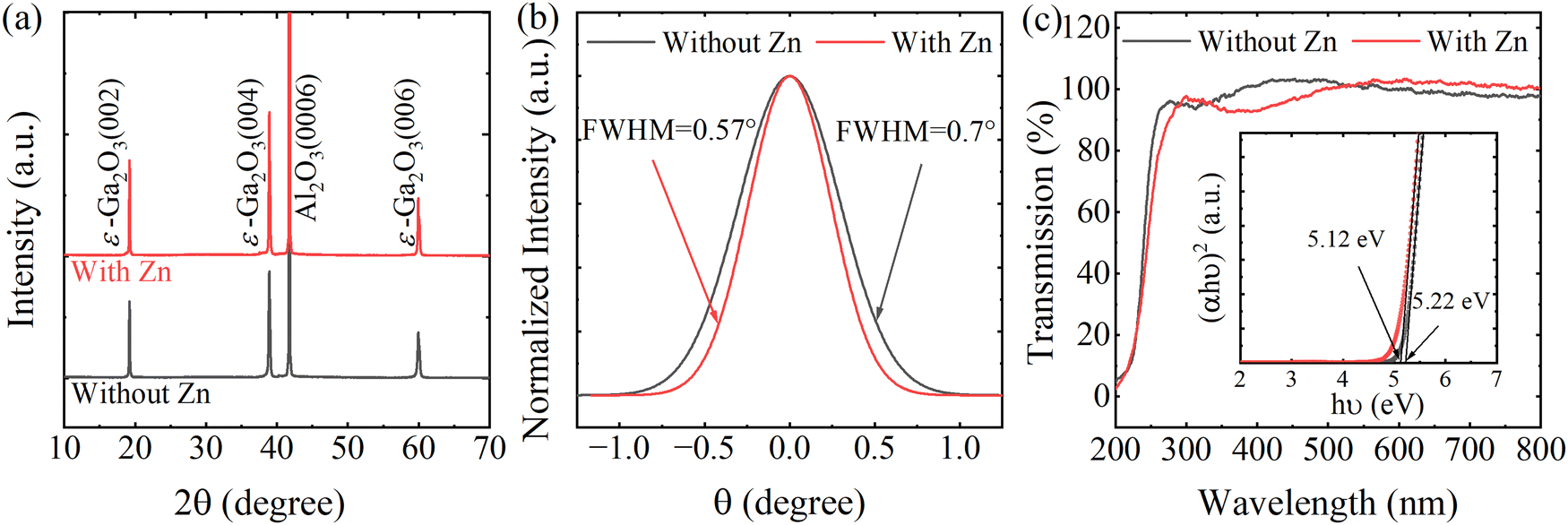 | ||
| Fig. 1 (a) XRD patterns, (b) normalized XRD rocking curves of (004) plane and (c) optical transmission spectra of ε-Ga2O3 films with and without Zn. | ||
Fig. 1(c) presents the optical transmission properties of the films. In the visible region, both the samples show greater than 85% of the average transmittance, and a sharp absorption edge can be observed at ∼250 nm. The relationship between (αhν)2 and photon energy (hν) is plotted (see the inset of Fig. 1c), where α is the absorption coefficient. The optical bandgap (Eg) of ε-Ga2O3 film and Zn-doped ε-Ga2O3 film can be determined to be 5.22 eV and 5.12 eV, respectively.
To analyze the chemical bond status of the samples, as shown in Fig. S3 (ESI†) and Fig. 2, XPS characterization has been performed on two films. Fig. 2(a) exhibits the high-resolution Ga 2p core-level spectra of the samples, and the peaks at 1117.4 eV and 1144.2 eV can be attributed to Ga 2p3/2 and Ga 2p1/2, respectively.30,42,43 After introducing Zn impurities, the Ga 2p3/2 and Ga 2p1/2 peaks did not shift, but they widened and weakened in intensity. This may be due to the substitution impurities changing the original state of the Ga atoms in the lattice. The observed spin–orbit splitting is ∼26.8 eV, which is very much in line with the previously reported ε-Ga2O3.44Fig. 2(b) shows the high-resolution Zn 2p core-level spectrum of a Zn-doped ε-Ga2O3 film. The Zn 2p3/2 and Zn 2p1/2 peaks can be obviously observed at 1021.3 and 1044.2 eV, respectively, indicating that Zn impurities have entered the crystal lattice well and participated in chemical bonding.45 To explore the state of O atoms in the lattice, the high-resolution O 1s core level spectra for the films are shown in Fig. 2(c). The peak with lower binding energy (OA) should be related to lattice oxygen (O2−), and the peak with higher binding energy (OB) corresponds to oxygen vacancies.22,46,47 As we can see, the OB peak of pure ε-Ga2O3 film is more pronounced, and tends to disappear after the introduction of Zn, indicating that the introduction of Zn inhibits the generation of oxygen vacancies.
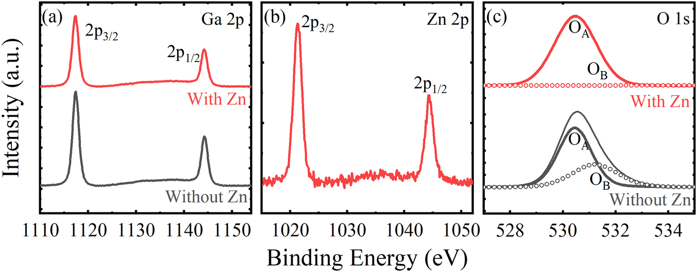 | ||
| Fig. 2 High-resolution XPS core-level spectra of (a) Ga 2p, (b) Zn 2p and (c) O 1s of the films. | ||
Fig. 3(a) gives the I–V characteristics of the photodetectors based on ε-Ga2O3 films with and without Zn in the dark and under 254 nm (680 μW cm−2) illumination. Clearly, the introduction of Zn could decrease the dark current and increase the light current at the same time. At 10 V, Zn-doped ε-Ga2O3 device has a low dark current of only 0.75 pA.
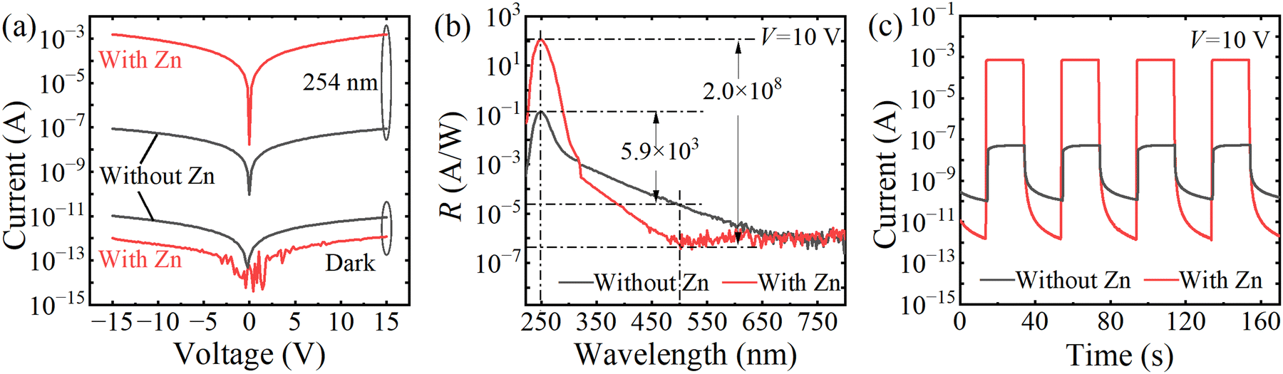 | ||
| Fig. 3 (a) I–V curves, (b) the response spectra, and (c) I–t curves of the devices. | ||
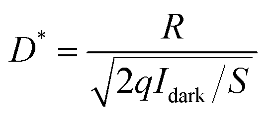
The photoresponse spectra of devices under 10 V bias are shown in Fig. 3(b). After the introduction of Zn impurities, the peak responsivity (Rpeak) at ∼250 nm significantly increased from 0.13 A W−1 to 118.7 A W−1. And the UV-visible rejection ratio (Rpeak/R500 nm) of a pure ε-Ga2O3 photodetector is only 5.9 × 10³, while that of the Zn-doped device can reach as high as 2.0 × 10⁸, indicating the excellent wavelength selectivity. Thanks to low dark current the high responsivity, the specific detectivity (D*) of the Zn-doped ε-Ga2O3 photodetector is calculated to be as high as 1.7 × 1016 cm Hz1/2 W−1 (Jones) using the following formula:
 | (1) |
Fig. 3(c) presents the I–t curves of solar-blind UV photodetectors at 10 V bias voltage under 254 nm light with an optical power density of 650 μW cm−2. Both devices have excellent repeatability and stability. Notably, after the introduction of Zn impurities, the on/off current ratio increases from 4.8 × 10² to 4.9 × 10⁸. Moreover, after switching off the light, the current of the Zn-doped ε-Ga2O3 solar-blind UV photodetector could completely recover to its initial dark state within 20 s, which is much better than that of the most early reported solar-blind UV photodetectors.13,15,49–51
The normalized transient photoresponse of the photodetector measured using an LED (255 nm) light source with different modulation frequencies of 0.1, 1, 10 and 100 Hz are shown in Fig. 4. With the increase in the modulation frequency, the photoresponse gradually decreases. The result shows that even at a high frequency of 100 Hz, the device can maintain high resolution and photoresponse over multiple cycles, confirming fast and reliable photo-switching. Moreover, 10–90% rise/decay times (tr/td) of the pure and Zn-doped ε-Ga2O3 devices can be estimated to be 255 ms/100 ms and 25 ms/32 ms, respectively.
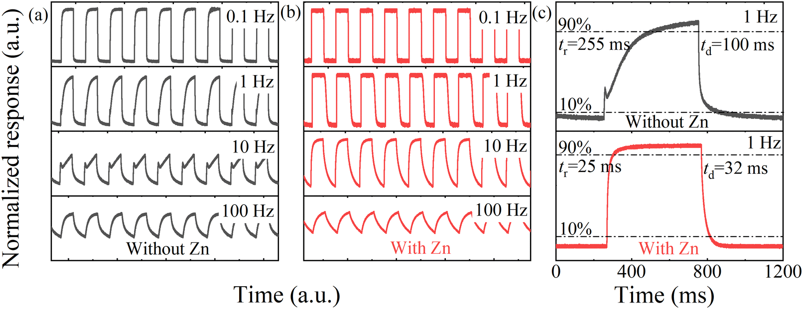 | ||
| Fig. 4 The transient photoresponse with different frequencies of the pure (a) and Zn-doped (b) ε-Ga2O3 devices; and (c) The transient photoresponse of the devices with frequencies of 1 Hz. | ||
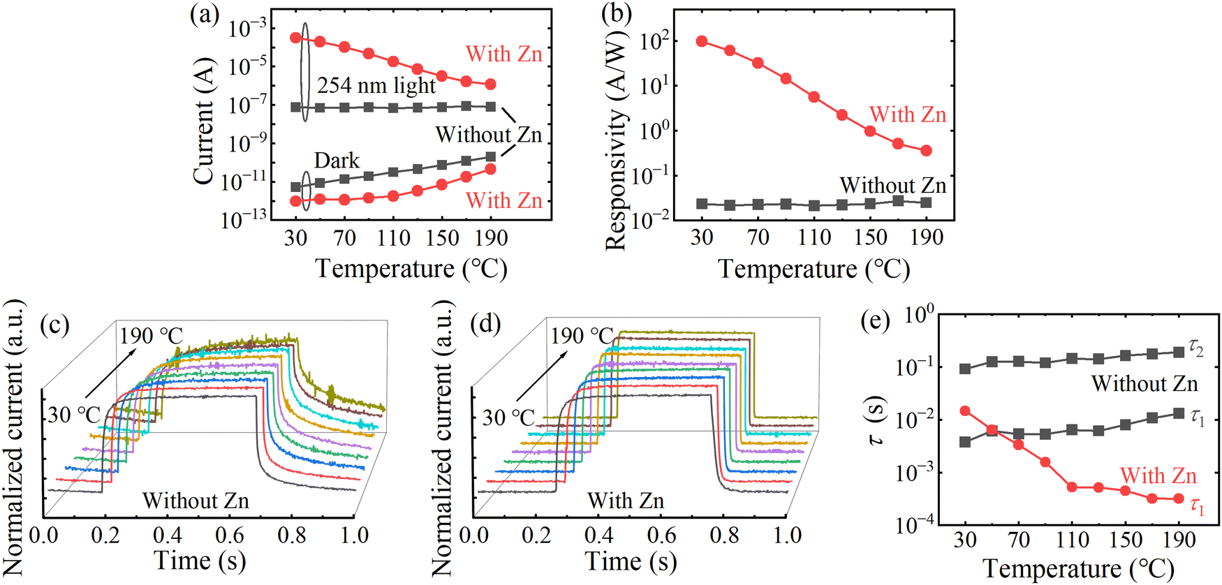
To further investigate the effect of Zn on the properties of ε-Ga2O3, the temperature dependent electronic and optoelectronic characteristics of ε-Ga2O3 devices without and with Zn have been tested and investigated at different temperatures. With increasing the temperature from 30 °C to 190 °C, the dark current of pure ε-Ga2O3 detector increases from 5 pA to 0.2 nA at 10 V, as shown in Fig. 5(a), and an exponential relationship between dark current and temperature can be observed due to thermal ionization of donor defects.52,53 As for the Zn-doped device, its dark current does not change much below 90 °C, but significantly increases with increasing temperature above 100 °C. This phenomenon should be associated with compensation effect and thermal ionization process of Zn impurities. Based on the current under 254 nm light illumination (650 μW cm−2) in Fig. 5(a), the responsivity of the devices at different temperatures has been calculated as shown in Fig. 5(b), and the Zn-doped device shows obvious photoconductive gain, while the pure ε-Ga2O3 detector has lower quantum efficiency. Moreover, the responsivity for the pure ε-Ga2O3 photodetector only undergoes minor change at 10 V with the increase of temperature, but the Zn-doped device shows a significant decrease.
 | ||
| Fig. 5 (a) The current and (b) responsivity as functions of operating temperature of the devices; The normalized transient photoresponse at different temperatures of the (c) pure and (d) Zn-doped ε-Ga2O3 devices; and (e) relaxation time constants as a function of operating temperature of the devices. | ||
To better understand the mechanism of the very different photoelectric characteristics of the two devices, the I–t curves were measured at 10 V bias voltage under various temperatures (see Fig. 5(c) and (d)). Clearly, with increasing the temperature, the response speed of Zn-doped detector increases significantly, while pure ε-Ga2O3 device gradually slows down. In addition, the decay curves of ε-Ga2O3 detectors with and without Zn can be well fitted to mono- and bi-exponential functions, respectively (see Fig. S4, ESI†). The mono- (eqn (2)) and bi-exponential (eqn (3)) decay equation are given below:
 | (2) |
 | (3) |
 | (4) |
Table 1 exhibits the comparison between our Zn-doped ε-Ga2O3 device and some reported ε-Ga2O3 thin film based solar-blind photodetectors. It is clear that our device has excellent overall performance. The superior photodetection performance of our device indicates that ε-Ga2O3 films doped/alloyed with Zn have great potential in practical applications of solar-blind photodetectors.
| Materials | Voltage (V) | UV-vis rejection ratio | Detectivity (Jones) | Response time tr/td (s) | Ref. |
|---|---|---|---|---|---|
| ε-Ga2O3 | 6 | — | 4.2 × 10¹⁴ | —/0.1 | 13 |
| ε-Ga2O3 | 6 | 1.2 × 10⁵ | 1.2 × 10¹⁵ | — | 29 |
| ε-Ga2O3 | 5 | 6 × 10³ | 1.2 × 10¹³ | 7.6/5.2 | 40 |
| ε-Ga2O3 | 5 | 1.8 × 10⁷ | 9.13 × 10¹⁴ | 0.05/0.09 | 30 |
| ε-Ga2O3 | 5 | 1.3 × 10⁴ | 1.67 × 10¹³ | 0.62/0.33 | 41 |
| ε-Ga2O3 | 5 | — | 4.37 × 10¹⁴ | 1.38/0.14 | 42 |
| ε-Ga2O3 | 2 | — | 2.49 × 10¹¹ | — | 44 |
| ε-Ga2O3: Sn | 20 | — | — | 0.41/0.16 | 48 |
| ε-Ga2O3: Mg | 5 | — | 2.85 × 10¹² | 1.6/5.4 | 49 |
| ε-Ga2O3: Al | 5 | — | 1.23 × 10¹³ | 2.09/0.49 | 42 |
| ε-Ga2O3 | 10 | 5.9 × 10³ | 7.3 × 10¹² | 0.225/0.1 | This work |
| Zn-doped ε-Ga2O3 | 10 | 2.0 × 10⁸ | 1.7 × 10¹⁶ | 0.025/0.032 | This work |
Conclusions
In a word, pure and 6.34 at% Zn-doped ε-Ga2O3 films were epitaxially grown by MOCVD on c-plane sapphire substrates, followed by face-to-face annealing in an oxygen atmosphere at 600 °C. It is obvious that the introduction of Zn can greatly improve the solar-blind UV detection performance of ε-Ga2O3 films. At room temperature, a low dark current of 0.75 pA, a high D* of 1.7 × 10¹⁶ Jones, and a large UV-visible rejection ratio of 2.0 × 10⁸ at 10 V bias have been demonstrated for the Zn-doped detector. Moreover, a fast response speed (tr = 25 ms, td = 32 ms) can be also observed and the current can attenuate by eight orders of magnitude and fully recover to the dark current state within 20 s after switching off the 254 nm light (650 μW cm−2). The temperature dependent photoelectronic characteristics of both pure and Zn-doped ε-Ga2O3 suggested that the excellent performance of our Zn-doped ε-Ga2O3 film device can be attributed to the introduction of Zn impurities, which improves the crystal quality and stability of the ε-Ga2O3 metastable structure and inhibits the formation of oxygen vacancies. Our results provide a new idea for the realization of Ga2O3-based high-performance solar-blind photodetectors.Author contributions
The manuscript was written through contributions of all authors. All authors have given approval to the final version of the manuscript.Conflicts of interest
The authors declare no competing financial interest.Acknowledgements
This work is supported by the National Natural Science Foundation of China (62074148, 61875194, 11727902, 12304111, and 12304112), the National Ten Thousand Talent Program for Young Top-notch Talents, the Key Research and Development Program of Changchun City (21ZY05), the Youth Innovation Promotion Association, CAS (2020225), the Jilin Province Young and Middle-aged Science and Technology Innovation Leaders and Team Project (20220508153RC), and the Jilin Province Science Fund (20220101053JC and 20210101145JC).References
- J. Yang, K. Liu, X. Chen and D. Shen, Prog. Quantum Electron., 2022, 83, 100397–100425 CrossRef.
- S. Surender, K. Prabakaran, S. Pradeep, I. D. Jacob, Y. F. Lu, S. Balakumar and K. Baskar, Opt. Mater., 2023, 136, 113462–113471 CrossRef CAS.
- W. Ruan and X. Meng, ACS Appl. Nano Mater., 2023, 1019–1026 CrossRef CAS.
- S. Park, Y. Yoon, H. Kim, T. Park, K. Kim and J. Hong, Nanomaterials, 2023, 13(5), 954–972 CrossRef CAS.
- B. Zhao, F. Wang, H. Chen, L. Zheng, L. Su, D. Zhao and X. Fang, Adv. Funct. Mater., 2017, 27(17), 1700264–1700271 CrossRef.
- Z. Li, T. Yan and X. Fang, Nat. Rev. Mater., 2023, 8(9), 587–603 CrossRef.
- Q. Cai, H. You, H. Guo, J. Wang, B. Liu, Z. Xie, D. Chen, H. Lu, Y. Zheng and R. Zhang, Light: Sci. Appl., 2021, 10(1), 94–124 CrossRef CAS.
- C. H. Kang, I. Dursun, G. Y. Liu, L. Sinatra, X. B. Sun, M. W. Kong, J. Pan, P. Maity, E. N. Ooi, T. K. Ng, O. F. Mohammed, O. M. Bakr and B. S. Ooi, Light: Sci. Appl., 2019, 8, 12–23 CrossRef.
- X. Zhu, Y. Wu, G. Li, K. Zhang, S. Feng and W. Lu, ACS Appl. Nano Mater., 2023, 6(3), 2048–2062 CrossRef CAS.
- Q. Zhang, N. Li, T. Zhang, D. Dong, Y. Yang, Y. Wang, Z. Dong, J. Shen, T. Zhou, Y. Liang, W. Tang, Z. Wu, Y. Zhang and J. Hao, Nat. Commun., 2023, 14(1), 418–426 CrossRef CAS PubMed.
- C. Zhang, K. Liu, Q. Ai, X. Sun, X. Chen, J. Yang, Y. Zhu, Z. Cheng, B. Li, L. Liu and D. Shen, Mater. Today Phys., 2023, 33, 101034–101039 CrossRef CAS.
- J. Yue, X. Ji, S. Li, X. Qi, P. Li, Z. Wu and W. Tang, Chin. Phys. B, 2023, 32(1), 016701–016706 CrossRef.
- Y. Qin, H. Sun, S. Long, G. S. Tompa, T. Salagaj, H. Dong, Q. He, G. Jian, Q. Liu, H. Lv and M. Liu, IEEE Electron Device Lett., 2019, 40(9), 1475–1478 CAS.
- X. Li, F. Xu, X. Wang, J. Luo, K. Ding, L. Ye, H. Li, Y. Xiong, P. Yu, C. Kong, L. Ye, H. Zhang and W. Li, Phys. Status Solidi RRL, 2023, 2200512–2200519 CrossRef.
- J. Yue, X. Ji, X. Qi, S. Li, Z. Yan, Z. Liu, P. Li, Z. Wu, Y. Guo and W. Tang, Vacuum, 2022, 203, 111270–111276 CrossRef CAS.
- Y. Yang, X. Y. Zhang, C. Wang, F. B. Ren, R. F. Zhu, C. H. Hsu, W. Y. Wu, D. S. Wuu, P. Gao, Y. J. Ruan, S. Y. Lien and W. Z. Zhu, Nanomaterials, 2022, 12(9), 1510–1522 CrossRef CAS PubMed.
- C. Wu, F. Wu, H. Hu, S. Wang, A. Liu and D. Guo, Mater. Today Phys., 2022, 28, 100883–100904 CrossRef CAS.
- Z. Hu, Q. Cheng, T. Zhang, Y. Zhang, X. Tian, Y. Zhang, Q. Feng, W. Xing, J. Ning, C. Zhang, J. Zhang and Y. Hao, J. Lumin., 2023, 255, 119596–119602 CrossRef CAS.
- C. Zhang, K. Liu, Q. Ai, X. Huang, X. Chen, Y. Zhu, J. Yang, Z. Cheng, B. Li, L. Liu and D. Shen, J. Phys. Chem. C, 2022, 126(51), 21839–21846 CrossRef CAS.
- R. Fornari, M. Pavesi, V. Montedoro, D. Klimm, F. Mezzadri, I. Cora, B. Pécz, F. Boschi, A. Parisini, A. Baraldi, C. Ferrari, E. Gombia and M. Bosi, Acta Mater., 2017, 140, 411–416 CrossRef CAS.
- A. Bosio, C. Borelli, A. Parisini, M. Pavesi, S. Vantaggio and R. Fornari, ECS J. Solid State Sci. Technol., 2020, 9(5), 055002–055007 CrossRef CAS.
- W. Chen, H. Luo, Z. Chen, Y. Pei, G. Wang and X. Lu, Appl. Surf. Sci., 2022, 603, 154440–154447 CrossRef CAS.
- W. Chen, Z. Chen, Z. Li, Z. Fei, Y. Pei, G. Wang and Z. He, Appl. Surf. Sci., 2022, 581, 152335–152343 CrossRef CAS.
- T. Zhang, Y. Li, Q. Cheng, Z. Hu, J. Ma, Y. Yao, C. Cui, Y. Zuo, Q. Feng, Y. Zhang, H. Zhou, J. Ning, C. Zhang, J. Zhang and Y. Hao, Superlattices Microstruct., 2021, 159, 107053–107060 CrossRef CAS.
- V. Montedoro, A. Torres, S. Dadgostar, J. Jimenez, M. Bosi, A. Parisini and R. Fornari, J. Mater. Sci. Eng. B, 2021, 264, 114918–114924 CrossRef CAS.
- S. Li, J. Yue, C. Lu, Z. Yan, Z. Liu, P. Li, D. Guo, Z. Wu, Y. Guo and W. Tang, Sci. China: Technol. Sci., 2022, 65(3), 704–712 CrossRef CAS.
- Y. Ma, T. Chen, X. Zhang, W. Tang, B. Feng, Y. Hu, L. Zhang, X. Zhou, X. Wei, K. Xu, D. Mudiyanselage, H. Fu and B. Zhang, ACS Appl. Mater. Interfaces, 2022, 14(30), 35194–35204 CrossRef CAS PubMed.
- Z.-Y. Yan, S. Li, Z. Liu, W.-J. Liu, F. Qiao, P.-G. Li, X. Tang, X.-H. Li, J.-Y. Yue, Y.-F. Guo and W.-H. Tang, IEEE J. Sel. Top. Quantum Electron., 2022, 28(2), 1–8 Search PubMed.
- Y. Qin, L. Li, X. Zhao, G. S. Tompa, H. Dong, G. Jian, Q. He, P. Tan, X. Hou, Z. Zhang, S. Yu, H. Sun, G. Xu, X. Miao, K. Xue, S. Long and M. Liu, ACS Photonics, 2020, 7(3), 812–820 CrossRef CAS.
- S. Li, J. Yue, X. Ji, C. Lu, Z. Yan, P. Li, D. Guo, Z. Wu and W. Tang, J. Mater. Chem. C, 2021, 9(16), 5437–5444 RSC.
- Y. Li, D. Zhang, R. Lin, Z. Zhang, W. Zheng and F. Huang, ACS Appl. Mater. Interfaces, 2019, 11(1), 1013–1020 CrossRef CAS.
- J. Jiang, J. Zhang and Z. Song, J. Lumin., 2020, 221, 117048–117052 CrossRef CAS.
- Z. Baji, I. Cora, Z. E. Horváth, E. Agócs and Z. Szabó, J. Vac. Sci. Technol., A, 2021, 39(3), 032411–032419 CrossRef CAS.
- D. Wang, K. Ge, D. Meng and Z. Chen, Mater. Lett., 2023, 330, 133251–133254 CrossRef CAS.
- K. Yamamura, L. Zhu, C. P. Irvine, J. A. Scott, M. Singh, A. Jallandhra, V. Bansal, M. R. Phillips and C. Ton-That, ACS Appl. Nano Mater., 2022, 5(9), 12087–12094 CrossRef CAS.
- X. Sun, K. Liu, X. Chen, Q. Hou, Z. Cheng, J. Yang, Q. Ai, Y. Zhu, B. Li, L. Liu and D. Shen, J. Mater. Chem. C, 2023, 11(9), 3227–3234 RSC.
- D. Guo, X. Qin, M. Lv, H. Shi, Y. Su, G. Yao, S. Wang, C. Li, P. Li and W. Tang, Electron. Mater. Lett., 2017, 13(6), 483–488 CrossRef CAS.
- V. Vasanthi, M. Kottaisamy and V. Ramakrishnan, Ceram. Int., 2019, 45(2), 2079–2087 CrossRef CAS.
- T. Yamanaka, Y. Hayashi and H. Takizawa, J. Ceram. Soc. Jpn., 2023, 131(4), 100–105 CrossRef CAS.
- X. Cao, Y. Xing, J. Han, J. Li, T. He, X. Zhang, J. Zhao and B. Zhang, Mater. Sci. Semicond. Process., 2021, 123, 105532–105537 CrossRef CAS.
- Z. Liu, Y. Huang, C. Zhang, J. Wang, H. Li, Z. Wu, P. Li and W. Tang, J. Phys. D: Appl. Phys., 2020, 53(29), 295109–295114 CrossRef CAS.
- Y. Gao, X. Tian, Q. Feng, X. Lu, C. Zhang, J. Zhang and Y. Hao, Ceram. Int., 2022, 48(15), 22031–22038 CrossRef CAS.
- H. He, C. Wu, H. Hu, S. Wang, F. Zhang, D. Guo and F. Wu, J. Phys. Chem. Lett., 2023, 14(28), 6444–6450 CrossRef CAS PubMed.
- Y. Yang, H. Zhu, L. Wang, Y. Jiang, T. Wang, C. Liu, B. Li, W. Tang, Z. Wu, Z. Yang and D. Li, Mater. Des., 2022, 221, 110944–110949 CrossRef CAS.
- K. Wu, L. Zhou, C. Mao and Y. Chu, Mater. Lett., 2023, 341, 134161–134164 CrossRef CAS.
- H. Qian, X. Zhang, Y. Ma, L. Zhang, T. Chen, X. Wei, W. Tang, X. Zhou, B. Feng, Y. Fan, Y. Sun and B. Zhang, Vacuum, 2022, 200, 111019–111026 CrossRef CAS.
- Y. Cheng, J. Ye, L. Lai, S. Fang and D. Guo, Adv. Electron. Mater., 2023, 9(4), 2201216–2201224 CrossRef CAS.
- Y. Cai, K. Zhang, Q. Feng, Y. Zuo, Z. Hu, Z. Feng, H. Zhou, X. Lu, C. Zhang, W. Tang, J. Zhang and Y. Hao, Opt. Mater. Express, 2018, 8(11), 3506–3517 CrossRef CAS.
- Z. Liu, Y. Huang, H. Li, C. Zhang, W. Jiang, D. Guo, Z. Wu, P. Li and W. Tang, Vacuum, 2020, 177, 109425–109429 CrossRef CAS.
- B. S. Qiao, Z. Z. Zhang, X. H. Xie, B. H. Li, X. Chen, H. F. Zhao, K. W. Liu, L. Liu and D. Z. Shen, J. Mater. Chem. C, 2021, 9(11), 4039–4045 RSC.
- G. Zeng, M.-R. Zhang, Y.-C. Chen, X.-X. Li, D.-B. Chen, C.-Y. Shi, X.-F. Zhao, N. Chen, T.-Y. Wang, D. W. Zhang and H.-L. Lu, Mater. Today Phys., 2023, 33, 101042–101049 CrossRef CAS.
- C. Xu, C. L. Senaratne, J. Kouvetakis and J. Menéndez, Appl. Phys. Lett., 2014, 105(23), 232103–232107 CrossRef.
- X. Zou, D. Xie, Y. Sun and C. Wang, Nano Res., 2022, 1–7 CAS.
Footnote |
| † Electronic supplementary information (ESI) available: SEM, XPS, EDS, time-dependent photocurrent characteristics. See DOI: https://doi.org/10.1039/d3tc03599a |
| This journal is © The Royal Society of Chemistry 2024 |