An ultraviolet, self-powered, and large area photodetector based on a n-SnO2/p-spiro-OMeTAD organic–inorganic heterojunction†
Received
25th September 2023
, Accepted 20th November 2023
First published on 22nd November 2023
Abstract
Self-powered photodetectors are of importance for practical applications. However, inorganic heterojunctions for photodetectors often contain defect states due to lattice mismatch. Herein, an ultraviolet photodetector based on a n-SnO2/p-spiro-OMeTAD organic–inorganic heterojunction (OIH) was fabricated by spin-coating. On the basis of spectral data (absorption, reflection, and ultraviolet photoemission spectra) and the Hall effect measurements, energy level alignment at the SnO2/spiro-OMeTAD interface is unveiled. The results of linear sweep voltammetry indicate that an ohmic contact is formed at the FTO/SnO2 interface. The responsivity and detectivity of the SnO2/spiro-OMeTAD photodetector are 1.42 mA W−1 and 3.10 × 10⁷ Jones at 386 nm with 30 W m−2, respectively. In addition, the performance of the device has no degradation for nearly 1000 hours. The working mechanism of the device based on SnO2/spiro-OMeTAD OIH is that when the device is irradiated with UV light, electrons transfer from the SnO2 layer to FTO, and holes transfer from the spiro-OMeTAD layer to Au. Finally, large area devices with 10 × 10 cm (active area 52 cm2) were prepared by the spraying method. In the rotating state, large area devices can effectively detect ultraviolet light. The device has potential to be applied as a high-performance, large-area ultraviolet photodetector.
1 Introduction
Self-powered photodetectors and photosensors play an important role in communication, military, health, and space exploration applications.1–5 SnO2 is an outstanding n-type semiconductor with high carrier mobility, low-temperature crystallinity, and ultraviolet (UV) sensitivity.6,7 Therefore, it is widely used as an electron transport layer in photovoltaics, photodetectors, diodes, etc.8,9 Photodetectors based on SnO2 inorganic heterojunctions (IHs) have been widely studied.10–12 A self-powered photodetector on the basis of a n-SnO2 microwire/p-InGaN IH was constructed, and it responded to ultraviolet-visible (330–530 nm) light irradiation.13 In addition, a photodetector based on SnO2/NiO IH was fabricated by depositing NiO using magnetron sputtering and SnO2 using the electron beam evaporation technique.14 Introducing an In2O3 interlayer into SnO2/SnS2 IH was also designed.2 A SnO2/MoS2 IH was fabricated by Sn sputtering followed by oxidation and depositing a MoS2 film by pulsed laser deposition.15 A SnO2 quantum dots/β-Bi2O3 nanofiber IH-based self-powered UV photodetector and an optical UV filter were also fabricated.16 A core–shell SnO2 microwire/CuZnS IH was constructed by simply coating a p-type (CuS)0.35:(ZnS)0.65 nanocomposite film (CuZnS) on a n-type SnO2 microwire.17 However, IHs often contain lattice mismatches at the interface, which reduce the performance and stability of the photodetector.18,19
In this study, we fabricated an ultraviolet photodetector based on a n-SnO2/p-spiro-OMeTAD organic–inorganic heterojunction (OIH) by spin-coating. The absorption, reflection, and ultraviolet photoemission spectra were obtained, the Hall effects were studied and the energy level alignment at the SnO2/spiro-OMeTAD interface was unveiled. Characterization using interface resistance, AFM, SEM, and cross-sectional SEM was also carried out. UV photodetectors were fabricated in a configuration of FTO/SnO2/spiro-OMeTAD/Au, with two different device areas; smaller with 0.35 cm × 0.4 cm and larger with 10 × 10 cm. Their optoelectronic properties and stability were studied.
2 Experimental
2.1 Fabrication of FTO/SnO2/spiro-OMeTAD/Au devices
The FTO conductive glass was cleaned in an ultrasonic cleaning machine for 15 min in the order of detergent, deionized water, and anhydrous ethanol. The electron transport layer was prepared on the cleaned FTO conductive glass. The solution obtained by diluting the SnO2 solution with deionized water 1![[thin space (1/6-em)]](https://www.rsc.org/images/entities/char_2009.gif) :6 was spin-coated on the FTO substrate for 30 s at a speed of 3000 rpm, and then annealed at 180 °C in an air environment for 30 min to form a dense layer of SnO2. 72.3 mg of spiro-MeOTAD was dissolved in 1 mL chlorobenzene solution. Then, 18 μL lithium-bis(trifluoromethanesulfonyl)imide (Li-TFSI) acetonitrile solution (520 mg mL−1), 20 μL tris(2-(1H-pyrazol-1-yl)-4-tert-butylpyridine)-cobalt(III) tris(bis(trifluoromethylsulfonyl)imide) (FK209 Co(III)-TFSI) acetonitrile solution (300 mg mL−1) and 29 μL 4-tert-butylpyridine (TBP) were added to the above solution and stirred at room temperature for 1 h to obtain spiro-MeOTAD solution. The solution was spin-coated on a SnO2 film at a speed of 2500 rpm by the dynamic spin coating method to prepare the hole transport layer. The device was oxidized in dry air for 12 h. Finally, the device was prepared by depositing a gold (Au) layer on the hole transport layer in a high vacuum of 10−4 Pa using resistive coating equipment (KC-ZD400).
:6 was spin-coated on the FTO substrate for 30 s at a speed of 3000 rpm, and then annealed at 180 °C in an air environment for 30 min to form a dense layer of SnO2. 72.3 mg of spiro-MeOTAD was dissolved in 1 mL chlorobenzene solution. Then, 18 μL lithium-bis(trifluoromethanesulfonyl)imide (Li-TFSI) acetonitrile solution (520 mg mL−1), 20 μL tris(2-(1H-pyrazol-1-yl)-4-tert-butylpyridine)-cobalt(III) tris(bis(trifluoromethylsulfonyl)imide) (FK209 Co(III)-TFSI) acetonitrile solution (300 mg mL−1) and 29 μL 4-tert-butylpyridine (TBP) were added to the above solution and stirred at room temperature for 1 h to obtain spiro-MeOTAD solution. The solution was spin-coated on a SnO2 film at a speed of 2500 rpm by the dynamic spin coating method to prepare the hole transport layer. The device was oxidized in dry air for 12 h. Finally, the device was prepared by depositing a gold (Au) layer on the hole transport layer in a high vacuum of 10−4 Pa using resistive coating equipment (KC-ZD400).
2.2 Preparation of large area FTO/SnO2/spiro-OMeTAD/Au devices
The SnO2 layer was formed by spraying SnO2 solution diluted with deionized water on 10 × 10 cm FTO conductive glass after cleaning and annealing at 180 °C for 30 min. Then, spiro-OMeTAD solution was sprayed on the SnO2 layer in an air environment to prepare the hole transport layer. Finally, a gold (Au) layer was deposited over the hole transport layer by thermal evaporation.
2.3 Characterization
The SEM analysis of devices was carried out using a scanning electron microscope (Thermo Fisher Scientific FIB-SEM GX4, USA). XRD analysis was carried out using a high-resolution diffractometer (SmartLab 9 kW, Rigaku, Japan). The Hall coefficient, conductivity, carrier concentration, carrier mobility, and carrier type of SnO2 films and spiro-OMeTAD films were measured using a Hall effect measurement system (MMR K2500, USA). The surface roughness of the device was tested using atomic force microscopy (MultiMode 8, Bruker Nano, USA). The contact angle of water droplets on FTO and SnO2 films was measured using a contact angle meter (Shanghai Zhongchen Digital Technology Apparatus Co., Ltd, JC2000C1, China). X-Ray photoelectron spectroscopy and ultraviolet photoelectron spectroscopy of films were carried out using an X-ray photoelectron spectrometer (Thermo Fisher Escalab Xi+, USA). As the excitation source, a helium Iα radiation light (21.22 eV) was used for UPS. A photoelectrochemical workstation system (ZAHNER CIMPS-2 pro, Germany) was used to investigate the photocurrent density–time performance and LSV of devices. The UV absorption and reflection spectra were obtained using a micro-spectrometer (ATP5020P, Optosky, China).
3 Results and discussion
3.1 SnO2/spiro-OMeTAD devices
3.1.1 Band gap and interfacial properties.
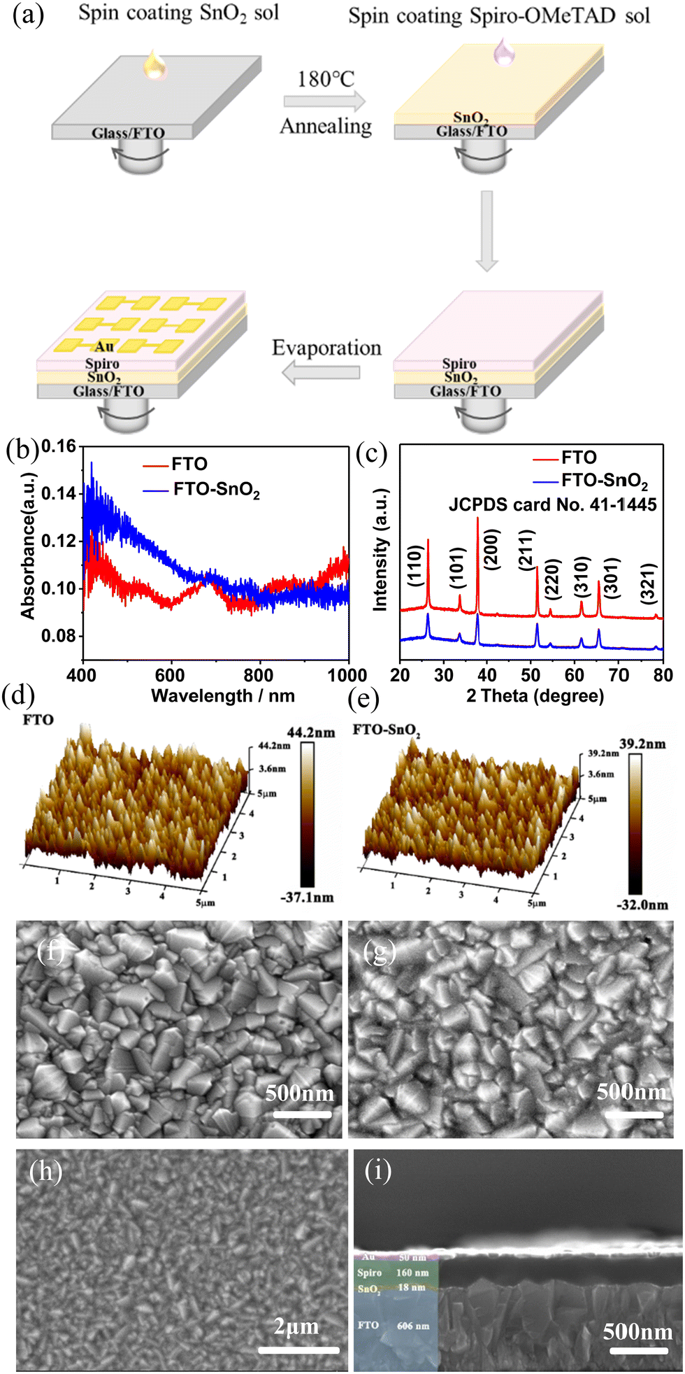
To determine the band gap (Eg) of the SnO2 powder (SnO2-P) and spiro-OMeTAD powder (spiro-OMeTAD-P), their ultraviolet-visible (UV-Vis) absorbance and reflection spectra were obtained. The UV-Vis absorption and reflection spectra of SnO2-P and spiro-OMeTAD-P are shown in Fig. S1a–d (ESI†), respectively. According to the Tauc plot method, the band gaps of SnO2 and spiro-OMeTAD are calculated to be 4.13 (Fig. S1e, ESI†) and 2.63 eV (Fig. S1f, ESI†), respectively. To obtain the valence band maximum (VBM), ultraviolet photoelectron spectra (UPS) of SnO2, spiro-OMeTAD, and Au film were measured (Fig. 1a). The binding energy cut-off (Ecutoff) values of SnO2, spiro-OMeTAD, and Au are 16.89, 17.73, and 17.13 eV, respectively, and the binding energy starting (Eonset) values are 2.78, 1.43, and 0.00 eV, respectively. According to VBM = −hν − (Ecutoff − Eonset)/WF = −hν − (Ecutoff − Eonset), where WF represents the work function, the VBM of SnO2 and spiro-OMeTAD are −7.11 and −4.49 eV, respectively, and the work functions of FTO and Au are −4.60 and −4.09 eV, respectively.20,21 Thus, the extrapolated conduction band minimum (CBM) values of SnO2 and spiro-OMeTAD are −2.98 and −1.86 eV, respectively. Using the UPS analysis results, the energy level diagrams of FTO/SnO2/spiro-OMeTAD/Au are drawn as shown in Fig. 1b. To measure the Hall effect of SnO2 thin films (SnO2-TFs) and spiro-OMeTAD-TFs, they were spin-coated on non-conductive glass, and their four corners were covered by a copper electrode using an evaporation method, as shown in Fig. 1c. The schematic diagram of the Hall effect is shown in Fig. 1d. The mechanism of the Hall effect to determine the type of semiconductor is as follows: when the applied current passes through the semiconductor as shown in the following figure, the carriers in the semiconductor (n-type semiconductors are electrons, p-type semiconductors are holes) are deflected by the Lorentz force. Therefore, electrons and holes are concentrated on both sides of the semiconductor, resulting in the formation of a potential between the two sides of the semiconductor. Therefore, p-type and n-type semiconductors can be determined based on the positive and negative potentials. As shown in Tables 1 and 2, the mobility of SnO2-TFs is −407.8 cm2 V−1 s−1, which indicates that SnO2-TFs is an n-type semiconductor. The mobility of spiro-OMeTAD-TFs is 432.66 cm2 V−1 s−1, which indicates that spiro-OMeTAD-TFs is a p-type semiconductor. It is speculated that a p–n heterojunction is formed at the interface between p-type spiro-OMeTAD and n-type SnO2.22–24 Its built-in field is 0.43 V as shown in Mott–Schottky curves (Fig. S2, ESI†). We compared the linear sweep voltammetry (LSV) curves of the different device structures of FTO/Au (Fig. 1e), FTO/SnO2/Au (Fig. 1f), FTO/spiro-OMeTAD/Au (Fig. 1g), and FTO/SnO2/spiro-OMeTAD/Au (Fig. 1h). The LSV curves of FTO/Au and FTO/SnO2/Au are almost coincident, indicating that SnO2 has good conductivity and ohmic contact at the interface between FTO, SnO2, and Au. The current of FTO/spiro-OMeTAD/Au and FTO/SnO2/spiro-OMeTAD/Au is close, which further indicates ohmic contact at the interface of FTO and SnO2. Due to the good conductivity of FTO, a Schottky junction is formed at the interfaces between FTO and the SnO2 thin film.
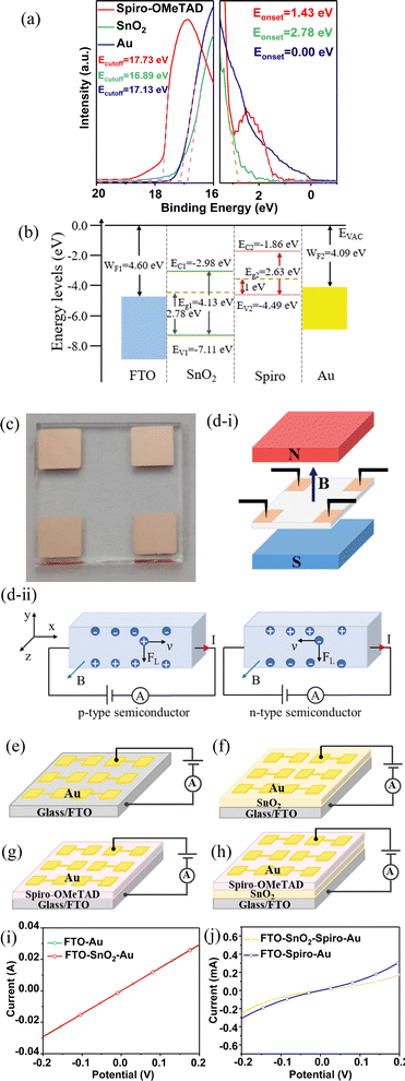 |
| | Fig. 1 (a) UPS spectra of SnO2, spiro-OMeTAD, and Au: secondary electrons’ cut-off edge and valence band spectrum. (b) Energy level diagrams of FTO, SnO2, spiro-OMeTAD, and Au. (c) Photographs of copper plating on four corners of SnO2-TFs by evaporation. (d) Schematic diagram of the Hall effect. Device structures of FTO/Au (e), FTO/SnO2/Au (f), FTO/spiro-OMeTAD/Au (g), and FTO/SnO2/spiro-OMeTAD/Au (h). (i) LSV curves of FTO/Au and FTO/SnO2/Au. (j) LSV curves of FTO/spiro-OMeTAD/Au and FTO/SnO2/spiro-OMeTAD/Au. | |
Table 1 Hall parameters of the SnO2 film at 297.0 K (8000 G field intensity)
| Description |
Mobility (cm2 V−1 s−1) |
Density (cm−3) |
Hall coeff. (cm−3 coul−1) |
Carrier type |
| SnO2 |
−407.80 |
−6.42 × 10¹² |
−1.00 × 10⁶ |
Electrons |
Table 2 Hall parameters of the spiro-OMeTAD film at 294.0 K (8000 G field intensity)
| Description |
Mobility (cm2 V−1 s−1) |
Density (cm−3) |
Hall coeff. (cm−3 coul−1) |
Carrier type |
| Spiro-OMeTAD |
432.66 |
−2.19 × 10¹¹ |
−2.85 × 10⁷ |
Holes |
3.1.2 Optical, phase, and morphological analyses.
The photodetector was fabricated by spin-coating in a configuration of FTO/SnO2/spiro-OMeTAD/Au, as shown in Fig. 2a. First, the optical properties of SnO2-TFs were investigated. We collected the UV-Vis absorbance spectra of FTO and SnO2-TFs deposited on FTO substrates (Fig. 2b). The peaks at 26.61, 33.89, and 51.78 degrees of the SnO2 powder obtained by volatilizing SnO2 solution at 180 °C correspond to the (110), (101), and (211) crystal planes, respectively, matching with the JCPDS 41-1445 card (Fig. S3a, ESI†).25 A large number of diffraction peaks can be observed in the XRD pattern of the spiro-OMeTAD powder, which indicates that the spiro-OMeTAD molecules are capable of self-assembling into a crystalline material (Fig. S3b, ESI†). No strong peaks are observed for SnO2 (Fig. S3c, ESI†) and spiro-OMeTAD films (Fig. S3d, ESI†). Compared with FTO-TFs, SnO2-TFs exhibit enhanced absorption in the wavelength range of 400–800 nm. The crystallinity of SnO2-TFs was analyzed by powder X-ray diffraction (PXRD) and the PXRD patterns are shown in Fig. 2c. Compared with that of FTO-TFs, no new diffraction peaks appeared. The covering of SnO2-TFs leads to a weakening of the diffraction intensity of FTO. The diffraction peaks of FTO originate from the tetragonal rutile SnO2 structure (JCPDS no. 41-1445).25 The peaks at 26.37, 33.63, 37.70, 52.48, 54.54, 61.53, 65.53, and 78.3 degrees correspond to the (110), (101), (200), (211), (220), (310), (301), and (321) crystal planes, respectively. To characterize the surface morphology of FTO and SnO2-TFs, the roughness (Fig. 2d and e) of FTO and SnO2-TFs was measured using an atomic force microscope (AFM). The root mean square roughness (Rq) values of the FTO substrate and SnO2-TFs are 11.7 and 10.2 nm, respectively. The average roughness (Ra) of the FTO substrate and SnO2-TFs is 9.29 and 8.13 nm, respectively. The reason for the low Rq and Ra values of SnO2-TFs is that the coverage of the film reduces the undulation of the FTO surface. The scanning electron microscopy (SEM) images of FTO (Fig. 2f), SnO2-TFs (Fig. 2g), and spiro-OMeTAD-TFs (Fig. 2h) were analyzed. It is found that the FTO surface is composed of several polygonal crystals. The coverage of SnO2-TFs caused the SEM image of the FTO to become blurred. The cross-sectional SEM image of the device (Fig. 2i) shows that the thicknesses of the SnO2-TFs, spiro-OMeTAD-TFs, and Au layers are 18, 160, and 50 nm, respectively.
 |
| | Fig. 2 (a) Schematic diagram of the preparation process of the FTO/SnO2/spiro-OMeTAD/Au device. (b) UV-Vis absorption spectra of FTO and SnO2-TFs. (c) XRD patterns of FTO and SnO2-TFs. AFM images of FTO (d) and SnO2-TFs (e). SEM images of FTO (f), FTO/SnO2-TFs (g), and FTO/SnO2/spiro-OMeTAD-TFs (h). (i) SEM images of the cross-section of the FTO/SnO2/spiro-OMeTAD/Au device. | |
3.1.3 Photoelectronic properties.
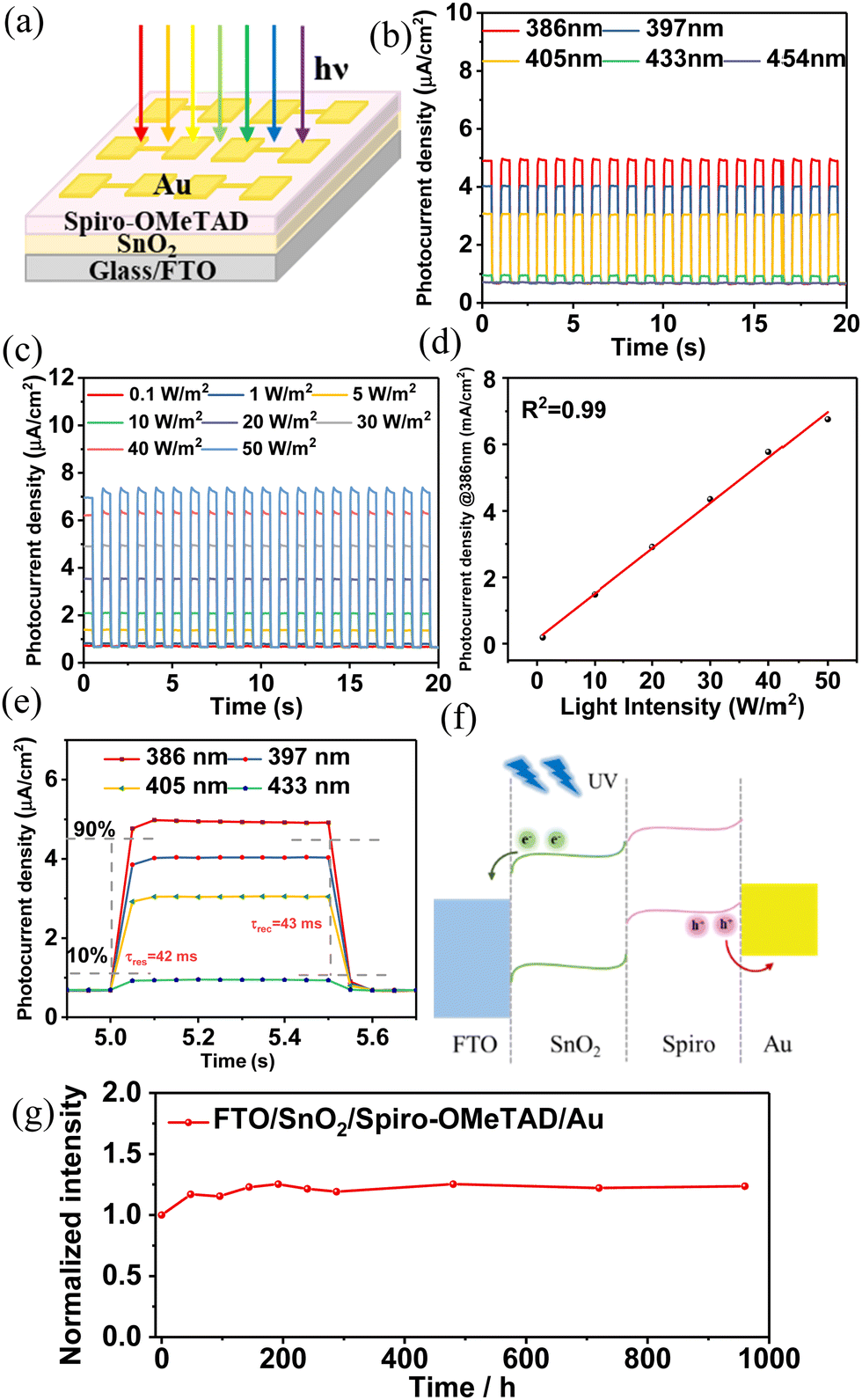
A schematic diagram of the FTO/SnO2/spiro-OMeTAD/Au device is shown in Fig. 3a. The photoelectronic properties of the FTO/SnO2/spiro-OMeTAD/Au devices were analysed. The J–t curves of the device were measured at different wavelengths (386, 397, 405, 433, and 454 nm) with a light intensity of 30 W m−2 (Fig. 3b). The device exhibits the best photocurrent response at 386 nm. The photocurrent response gradually decreases with increasing wavelength, and becomes weak beyond 454 nm, indicating that the SnO2/spiro-OMeTAD device has a high photocurrent response in the ultraviolet region. The working wavelength of SnO2/spiro-OMeTAD OIH is 386–433 nm. The photocurrent density of the device reaches 4.25 μA cm−2 at 386 nm with 30 W m−2. To further investigate the photoelectric sensitivity of the device, we measured the photocurrent response at 386 nm with different light intensities (Fig. 3c). The results show that the device is capable of producing a regular response to a low intensity of 1 W m−2. In addition, the device can produce a linear response (R2 = 0.99) to different light intensities (0.1 to 50 W m−2), as shown in Fig. 3d, which facilitates the estimation of light and electrical signals. Fig. 3e shows an enlarged view of the device's response period at 386–433 nm. At 386 nm, the response time (τres) and recovery time (τrec) are 42 and 43 ms, respectively.26 In addition, we will investigate whether there is a charge trapping mechanism in a future work. Responsivity (R) is one of the important performance indicators of photodetectors, R = (IPC − IDark)/S × P, where IPC is the photocurrent, IDark is the dark-current, S is the illumination area and P is the illumination intensity.27 The detectivity (D*) is also another key parameter, D* = R/(2eJDark)0.5, where e is the electron charge and JDark is the dark current density.28 Based on the above equations, the R and D* values calculated for the device at 386 nm with 30 W m−2 are 1.42 mA W−1 and 3.10 × 10⁷ Jones, respectively. A comparison of the performance of our detectors and related detectors that have been published is shown in Table 3. The energy band bending diagram of the photodetector based on SnO2/spiro-OMeTAD OIH is shown in Fig. 3f. The device of FTO/spiro-OMeTAD/Au has no photoelectric response, indicating that the photons absorbed by spiro-OMeTAD cannot be converted into electrons (Fig. S4, ESI†). Thus, the working mechanism of the photodetector based on SnO2/spiro-OMeTAD OIH is as follows: when the device is irradiated with UV light, electrons transfer from the SnO2 layer to FTO, and holes transfer from the spiro-OMeTAD layer to Au. In addition, the stability of the photodetector was investigated, and the normalization curve is shown in Fig. 3g. The results show that the performance of the device has no degradation for nearly 1000 hours, which indicates the device exhibits good stability. The device is prepared by the solution method, and its stability may be improved due to self-adjustment between the interfaces. In addition, the oxidation of spiro-OMeTAD is also a reason for the gradual increase in performance.
 |
| | Fig. 3 The performance of the photodetector based on SnO2/spiro-OMeTAD OIH. (a) Schematic diagram of J–t measurement. (b) J–t curves at different wavelengths with 30 W m−2. (c) J–t curve at 386 nm with different light intensities. (d) Normalized curves of photocurrent density under different light intensities. (e) Enlarged image of the single response period of the device shown in Fig. 3(c) at wavelengths of 386–433 nm to obtain its response time and recovery time. (f) Band bending diagram. (g) The normalized curve for the stability of the devices. | |
Table 3 Performance of self-powered photodetectors based on SnO2/spiro-OMeTAD OIH
| Photodetector |
Bias (V) |
Responsivity (R/mA W−1) |
Detectivity (D*/Jones) |
Applied conditions |
Ref. |
| SnO2/Mg:SnO2 |
0 |
1.55 |
9.8 × 10¹⁰ |
290 nm, 0.1177 W m−2 |
29
|
| SnO2 microwire/InGaN |
0 |
152.5 |
3.77 × 10¹² |
360 nm |
13
|
| F-SnO2/ZnS |
0 |
24 |
15.10 × 10¹⁰ |
UV |
30
|
| SnO2/In2O3/SnS2 |
0 |
2.9 |
5.9 × 10⁷ |
1.4 mW cm−2 |
2
|
| NiO TF/SnO2 TF |
0 |
0.141 |
2.8 × 10⁸ |
365 nm |
14
|
| SnO2/MoS2 |
0 |
350 |
1.25 × 10¹¹ |
900 nm, 0.025 mW cm−2 |
15
|
| SnO2/CuZnS core–shell microwire |
0 |
1.6 |
— |
315 nm |
17
|
| SnO2/spiro-OMeTAD |
0 |
1.42 |
3.10 × 10⁷ |
386 nm, 30 W m−2 |
This work |
3.2 Large area devices
Large area devices (FTO/SnO2/spiro-OMeTAD/Au) with 10 × 10 cm (active area 52 cm2) were prepared by the spraying method, and the preparation process is shown schematically in Fig. 4a. Subsequently, 9 positions of the large-area device were selected (Fig. 4b) to measure their performance at 386 nm with 30 W m−2. It is found that the photocurrents generated at different positions of the device do not differ significantly and are relatively uniform (Fig. 4c and d). To evaluate the all-around detection performance of the device similar to a radar in actual work, the device is rotated, and the UV lamp is fixed at a fixed angle to simulate the UV signal. A schematic of the rotation testing of the device is shown in Fig. 4e. The J–t performance of the device in the rotating state under UV illumination (white light as a reference) is shown in Fig. 4f. The spectral profiles of UV and white light are presented in Fig. S5a and b (ESI†). The device has no significant response to white light as shown in Fig. 4f. Thus, it is visible blind. In contrast, there is a regular response when the device is irradiated with UV light. Fig. 4f is a zoomed in image from 476 to 485 s. The J–t curve detected during rotation presents a triangular profile (the rising curve represents the UV light, and the falling curve represents the reverse UV light), as shown in Fig. 4g.
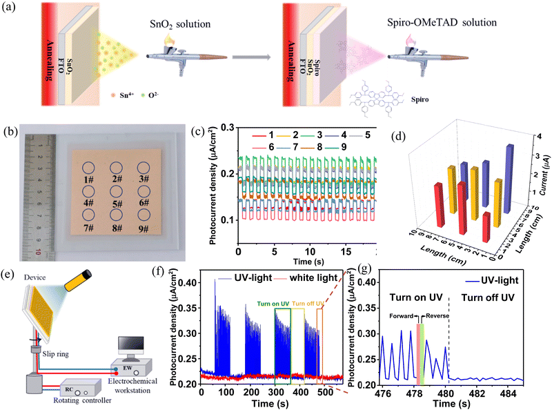 |
| | Fig. 4 The performance of the large area photodetector based on SnO2/spiro-OMeTAD OIH. (a) Schematic diagram of the preparation process of a 10 × 10 cm large area device. (b) Photographs of large area devices. (c) J–t curves at 9 positions of the device. (d) Current distribution diagram at 9 positions of the device. (e) Schematic diagram of rotation testing for the large-scale device. (f) J–t curve for rotation measurement. (g) Enlarged image of the J–t curve. | |
4 Conclusions
In summary, in this study, we used SnO2 and spiro-OMeTAD thin films to form an OIH self-powered ultraviolet photodetector. The results indicate that the device exhibits a high photocurrent response in the ultraviolet region. The device exhibits good stability and large-area devices can be prepared, which indicates that our work provides a simple and effective method for preparing large-area high-performance optoelectronic devices.
Conflicts of interest
There are no conflicts to declare.
Acknowledgements
This work was financially supported by the Shandong Province Natural Science Foundation (Grant No. ZR2019MB021).
Notes and references
- M. Xu, Z. Xu, Z. Sun, W. Chen, L. Wang, Y. Liu, Y. Wang, X. Du and S. Pan, ACS Appl. Mater. Interfaces, 2023, 15, 3664–3672 CrossRef CAS.
- S. Abbas, D.-K. Ban and J. Kim, Sens. Actuators, A, 2019, 293, 215–221 CrossRef CAS.
- Z. Li, T. Yan and X. Fang, Nat. Rev. Mater., 2023, 8, 587–603 CrossRef.
- W. Song, J. Chen, Z. Li and X. Fang, Adv. Mater., 2021, 33, 2101059 CrossRef CAS PubMed.
- Y. Chen, L. Su, M. Jiang and X. Fang, J. Mater. Sci. Technol., 2022, 105, 259–265 CrossRef CAS.
- S. O. Abdulghani, E. Y. Salih and A. S. Mohammed, Mater. Chem. Phys., 2023, 303, 127859 CrossRef CAS.
- Y. Zhang, W. Xu, X. Xu, J. Cai, W. Yang and X. Fang, J. Phys. Chem. Lett., 2019, 10, 836–841 CrossRef CAS PubMed.
- S. Kim, H. Lim, S. Kim, B. Pandit, J. Cho and H. C. Kang, J. Alloys Compd., 2023, 963, 171265 CrossRef CAS.
- N. Tugluoglu, S. Eymur and N. Turan, J. Mater. Sci.: Mater. Electron., 2023, 34, 160 CrossRef CAS.
- S. Fu, R. Song, Y. Wang, Y. Han, C. Gao, J. Ma, H. Xu, B. Li, A. Shen and Y. Liu, Adv. Mater. Interfaces, 2023, 10, 2202488 CrossRef CAS.
- T. Xu, M. Jiang, P. Wan, Y. Liu, C. Kan and D. Shi, J. Mater. Sci. Technol., 2023, 138, 183–192 CrossRef CAS.
- H. Yu, L. Qu, M. Zhang, Y. Wang, C. Lou, Y. Xu, M. Cui, Z. Shao, X. Liu, P. Hu and W. Feng, Adv. Opt. Mater., 2023, 11, 2202341 CrossRef CAS.
- Y. Zhang, T. Xu, K. Chang, S. Cao, P. Wan, D. Shi, C. Kan and M. Jiang, Results Phys., 2022, 42, 105995 CrossRef.
- M. Athira, S. P. Bharath and S. Angappane, Sens. Actuators, A, 2022, 340, 113540 CrossRef CAS.
- P. Augustine, K. L. Kumawat, D. K. Singh, S. B. Krupanidhi and K. K. Nanda, Appl. Phys. Lett., 2022, 120, 181106 CrossRef CAS.
- S. Praveen, S. Veeralingam and S. Badhulika, Adv. Mater. Interfaces, 2021, 8, 2100373 CrossRef CAS.
- J. Cai, X. Xu, L. Su, W. Yang, H. Chen, Y. Zhang and X. Fang, Adv. Opt. Mater., 2018, 6, 1800213 CrossRef.
- X. Liu, D. Cao, Y. Yao, P. Tang, M. Zhang, X. Chen and H. Shu, J. Mater. Chem. C, 2022, 10, 1984–1990 RSC.
- Z. Zhang, Y. Ning and X. Fang, J. Mater. Chem. C, 2019, 7, 223–229 RSC.
- K. Zou, Q. Li, J. Fan, H. Tang, L. Chen, S. Tao, T. Xu and W. Huang, ACS Mater. Lett., 2022, 4, 1101–1111 CrossRef CAS.
- S. S. Mali, J. V. Patil, S. R. Rondiya, N. Y. Dzade, J. A. Steele, M. K. Nazeeruddin, P. S. Patil and C. K. Hong, Adv. Mater., 2022, 34, 2203204 CrossRef CAS.
- K. Shehzad, T. Shi, A. Qadir, X. Wan, H. Guo, A. Ali, W. Xuan, H. Xu, Z. Gu, X. Peng, J. Xie, L. Sun, Q. He, Z. Xu, C. Gao, Y.-S. Rim, Y. Dan, T. Hasan, P. Tan, E. Li, W. Yin, Z. Cheng, B. Yu, Y. Xu, J. Luo and X. Duan, Adv. Mater. Technol., 2017, 2, 1600262 CrossRef.
- Y. Xu, A. Ali, K. Shehzad, N. Meng, M. Xu, Y. Zhang, X. Wang, C. Jin, H. Wang, Y. Guo, Z. Yang, B. Yu, Y. Liu, Q. He, X. Duan, X. Wang, P.-H. Tan, W. Hu, H. Lu and T. Hasan, Adv. Mater. Technol., 2017, 2, 1600241 CrossRef.
- X. Chen, K. Shehzad, L. Gao, M. Long, H. Guo, S. Qin, X. Wang, F. Wang, Y. Shi, W. Hu, Y. Xu and X. Wang, Adv. Mater., 2020, 32, 1902039 CrossRef CAS.
- L. Xiong, M. Qin, G. Yang, Y. Guo, H. Lei, Q. Liu, W. Ke, H. Tao, P. Qin, S. Li, H. Yu and G. Fang, J. Mater. Chem. A, 2016, 4, 8374–8383 RSC.
- S. Chen, K. Shehzad, X. Qiao, X. Luo, X. Liu, Y. Zhang, X. Zhang, Y. Xu and X. Fan, J. Mater. Chem. C, 2018, 6, 11078–11085 RSC.
- Q. Zhang, N. Li, T. Zhang, D. Dong, Y. Yang, Y. Wang, Z. Dong, J. Shen, T. Zhou, Y. Liang, W. Tang, Z. Wu, Y. Zhang and J. Hao, Nat. Commun., 2023, 14, 418 CrossRef CAS.
- C. Ling, B. Feng, X. Wang, L. Zhang, T. Zhang, M. Cao, D. Yu, X. Xue, Q. Xue, J. Zhang, C. Wang, L. Zhu, H. Lu and W. Liu, J. Mater. Chem. C, 2022, 10, 2049–2059 RSC.
- B. H. Liu, M. K. Li, W. Fu, P. Ye, E. Wentao, X. L. Xiao, H. R. Wei and Y. M. Lu, Opt. Mater., 2022, 129, 112571 CrossRef CAS.
- J. A. Salam and R. Jayakrishnan, J. Mater. Sci., 2023, 58, 5186–5207 CrossRef CAS.
|
| This journal is © The Royal Society of Chemistry 2024 |
Click here to see how this site uses Cookies. View our privacy policy here. 
 *,
Jie
Yin
* and
Xianxi
Zhang
*
*,
Jie
Yin
* and
Xianxi
Zhang
*