
A review on diverse streams of interface engineering for organic thin-film transistors
Jin-Hyuk
Kwon
a,
Min-Hoi
Kim
 *ab and
Jin-Hyuk
Bae
*c
*ab and
Jin-Hyuk
Bae
*c
aResearch Institute of Printed Electronics & 3D Printing, Industry University Cooperation Foundation, Hanbat National University, Daejeon 34158, Republic of Korea. E-mail: mhkim8@hanbat.ac.kr
bDepartment of Creative Convergence Engineering, Hanbat National University, Daejeon 34158, Republic of Korea
cSchool of Electronic and Electrical Engineering, Kyungpook National University, Daegu 41566, Republic of Korea. E-mail: jhbae@ee.knu.ac.kr
First published on 20th November 2023
Abstract
Organic thin-film transistors (OTFTs) offer a promising solution for facile, low-cost, and large-area fabrication of electronic circuitry. In the development of OTFTs, interface engineering has been essential for modulating the properties of the interfaces between the semiconductor and gate insulator and between the semiconductor and source–drain electrodes. It is worth noting that advancements in OTFTs have accompanied the dynamic subdivision of the field, with diverse technological streams focused on interface engineering. These streams include interface engineering for conventional OTFTs, memory OTFTs, sensor OTFTs, and others. As the differentiation and progress of interface engineering can, in turn, play a pivotal role in enhancing the applicability of OTFTs, it is informative to discern the diverse technological streams of multidimensional interface engineering. In this review article, we provide a critical overview of interface engineering for OTFTs, highlighting the technological diversity and varied purposes of interface engineering for different OTFT applications. We also explain the principles and mechanisms behind controlling the performance of OTFTs through interface engineering. This review will contribute to building useful insights into the design and improvement of OTFTs, as well as deepening understanding of molecular interactions and charge-carrier behaviours in these devices.
 Jin-Hyuk Kwon | Jin-Hyuk Kwon received his PhD degree in Electronic and Electrical Engineering at Kyungpook National University in 2021. Currently he is a postdoctoral researcher in the Research Institute of Printed Electronics & 3D Printing, Hanbat National University. His research interests focus on interfacial phenomena associated with electronic and molecular behaviours in solution-processed organic and metal oxide-based thin-film transistors. |
 Min-Hoi Kim | Min-Hoi Kim received his PhD degree in electronic engineering at Seoul National University in 2013. Now he is a professor in the Department of Creative Convergence Engineering, Hanbat National University. His research interests focus on organic and oxide electronic devices including memory and sensor and solution-processes for electronic microfabrication. |
 Jin-Hyuk Bae | Jin-Hyuk Bae received his PhD degree in electrical engineering from the Seoul National University, Seoul, South Korea, in 2010. From 2010 to 2012, he worked as a Postdoctoral Research Fellow at the Ecole Nationale Superiere des Mines de Saint-Etienne, Gardanne, France. In 2012, he joined the faculty with the School of Electronics Engineering, Kyungpook National University, where he is currently a Professor. His research interests include interfacial engineering and physics of organic based and metal-oxide-based electronic devices and their sensor applications. |
1. Introduction
Over the past several decades, organic thin-film transistors (OTFTs) have sparked widespread interest due to their applicability in flexible or stretchable electronics, ability to be solution-processed, and promising electrical characteristics.1–5 OTFTs generally refer to TFT devices that utilize organic semiconductors (OSCs) as the active layer. The inherent flexibility of OSCs as a key requirement enables mechanical compatibility between OTFTs and plastic substrates, which has opened the door for various new-concept electronics including wearable components and systems.6–8 Moreover, the solution processability, which has been instrumental in the progress of printing technologies, is an appealing feature for cost-effective and large-scale circuit production. In order to fully harness the advantages of OTFTs and enable their practical application, the development of techniques aimed at improving the electrical characteristics of OTFTs has been essential. It is worth noting that the recent years have witnessed remarkable achievements in the electrical performance of OTFTs (Table 1).9–25| Organic semiconductor | Mobility (cm2 V−1 s−1) | Threshold voltage (V) | ON/OFF ratio | Ref. |
|---|---|---|---|---|
| C10-DNTT | 18 | −0.18 | ≈108 | 9 |
| C10-DNTT | 5.22 | −7.7 ± 0.97 | ≈106 | 10 |
| FM-C4 | 2.06 | −3 to −8 | ≈105 | 11 |
| Ph-DBA-C8 | 11.8 | −3 to −13 | ≈106 | 12 |
| DNTT | 15.3 | 4.6 | ≈107 | 13 |
| C8-BTBT | 15.4 | ≈−7 | ≈109 | 14 |
| pDFB-TF | 5.04 | 14.1 | ≈105 to ≈106 | 15 |
| C8-BTBT | 18.6 | −0.11 | ≈106 | 16 |
| C8-BTBT | 7.72 | −10.43 | ≈105 | 17 |
| DPh-DNTT | 14 | — | ≈108 | 18 |
| P(DPP2DT-TT) | 12.4 | −0.5 ± 0.5 | ≈105 | 19 |
| P(NDI3DP-Se2) | 10.1 | 0.5 ± 0.5 | ≈105 | |
| Fu-F | 2.79 | 7 to 10 | ≈106 to ≈107 | 20 |
| DPh-DNTT | 6.4 | −23.7 to −29.3 | ≈106 to ≈107 | 21 |
| TDPP-Se | 11.02 | 0 to −10 | ≈106 to ≈107 | 22 |
| PAQM-BT | 5.10 | −4 | ≈104 to ≈105 | 23 |
| C8-BTBT | 9.33 | — | ≈105 | 24 |
| TIIQ-b16 | 2.54 | 16.2 ± 7.23 | ≈105 to ≈106 | 25 |
Interface engineering has been a vital approach in the quest to modulate and/or improve the characteristics of various organic electronic devices, including OTFTs, organic light-emitting diodes (OLEDs), and organic photovoltaics (OPVs).26–35 Interface engineering in OTFTs often focuses on controlling and manipulating the electrical characteristics related to the switching function, while in OLEDs and OPVs, one of the key aspects of interface engineering is maximizing energy conversion for light emission and electricity generation, respectively.36,37 OTFTs incorporate multiple heterogeneous materials for the constituent layers, each with designed roles, which accompanies the formation of multiple interfaces between them. These interfaces exist as spatial regions where charge carriers can experience intended and/or unintended practical impacts. Hence, an electrical measurement result for OTFTs contains a composite of information on the charge behaviours at the multiple interfaces. In a structural aspect, OTFTs are typically constructed with two primary interfaces: one between the OSC and gate insulator (GI) and the other between the OSC and source–drain (SD) electrodes. Charge carriers pass through the primary interfaces, thereby forming the device current and enabling the device operation. Accordingly, the electrical characteristics of OTFTs strongly depend on the properties of the primary interfaces. Specifically, the dynamics of charge carriers at the primary interfaces determine the electrical characteristics of OTFTs.
The charge-carrier dynamics at the primary interfaces can be modulated by changing the properties of the primary interfaces.38–40 For OTFTs, interface engineering can be defined as a scientific and technological process that modifies the properties of interfaces to improve the electrical characteristics of OTFTs or introduce specific desired features into them. Interface engineering for OTFTs has adopted numerous methods so far, from selecting suitable materials to applying surface treatments, adding functional layers, or modifying various process conditions.41–43 As OTFTs are basically electronic devices that rely on the flow of electrons, the ultimate consideration in interface engineering is how charge carriers experience the interfaces. Interface engineering involves specific intrinsic or extrinsic driving forces, which determine the spatial distribution of molecules and the energetic distribution of electronic states. These conditions for molecules and states have a direct association with the effective properties of the primary interfaces that impact charge carriers. Therefore, a sophisticated understanding and utilization of possible driving forces are required for the purpose-based design of interface engineering.
For the ceaseless advancement of OTFTs, it is crucial to not only have a comprehensive understanding of interface engineering but also reach a more systematic understanding. Over time, the field of OTFTs has evolved with divisions into diverse subfields, including memory OTFTs and sensor OTFTs, with each subfield demonstrating high potential. This evolution has been accompanied by the technological diversity of interface engineering for OTFTs. That is, there exist distinct differences in the purpose and focus between the diverse streams of interface engineering. The state of technological diversity can serve as a catalyst for creative convergence and integration between different technologies and areas of knowledge, accelerating the progress of a field. It is thus necessary and useful to recognize the technological diversity of interface engineering and gain knowledge from the diverse streams. However, there is a notable deficiency in the systematic analysis and understanding of the diversified interface engineering for OTFTs.
This review categorizes interface engineering for OTFTs and analyzes each attribute, thereby illuminating its diverse streams. Firstly, the need for interface engineering in OTFTs is discussed in detail. Secondly, theories associated with interface engineering for OTFTs, as well as characterization methods, are summarized. Thirdly, the diverse streams of interface engineering are systematically discussed. Lastly, the review concludes with a summary and perspectives on the future direction of interface engineering for OTFTs.
2. The need for interface engineering
2.1. Impact of interfaces in OTFTs
The fundamental functionality of OTFTs is established by the presence of the primary interfaces between the OSC and GI and between the OSC and SD electrodes. The injection and transport of charge carriers at the primary interfaces are often considered critical for understanding the electrical characteristics of OTFTs. Specifically, a conducting pathway is created at the OSC–GI interface in OTFTs, when the applied gate voltage (VG) exceeds the threshold voltage (Vth).44,45 The conducting pathway serves as the channel, facilitating the transport of charge carriers such as electrons and holes. Note that OTFTs, as a subtype of field-effect transistors, contain a capacitor structure consisting of the gate electrode, insulator, and semiconductor. In p-type OSCs, a high concentration of holes is accumulated in the channel region, while in n-type OSCs, a high concentration of electrons is accumulated. Simultaneously, the injection and extraction of charge carriers occur locally at the OSC–SD interface under a potential difference between the source and drain electrodes.46 When possible leakages, such as gate current, are sufficiently negligible, the channel current is nearly equal in magnitude to the injection and extraction currents. In brief, the transport of charge carriers takes place at the OSC–GI interface, with charge carriers being injected and extracted at the OSC–SD interface, forming a continuous flow of charge carriers from the source to drain through the channel.The charge-carrier dynamics at the primary interfaces, namely the injection and transport processes obey (or can be understood through) specific mechanisms. The mechanisms for the charge-carrier dynamics, which can be likened to a clockwork with multiple gears, are complex arrangements of various underlying factors. These factors include the properties of the primary interfaces, as well as the inherent material features, device characteristic parameters, and measurement conditions; moreover, they are correlated with each other. As a result, the properties of the primary interfaces have a significant impact on the electrical characteristics of OTFTs.
2.2. Diversification and significance of interface engineering
Interface engineering has been considered instrumental in the development of OTFTs. The electrical characteristics of OTFTs are shaped by mechanisms for the charge-carrier dynamics at the primary interfaces, i.e., the OSC–GI interface and OSC–SD interface. When the properties of the primary interfaces change, these mechanisms can be modulated or acquire new features. Since it is possible to implement mechanisms tailored to specific purposes, numerous attempts have been made to functionalize OTFTs in a wide variety of forms. It is worth noting that interface engineering has been diversified, opening up new possibilities for OTFTs. Through the diversification of interface engineering, various types of OTFTs, such as conventional OTFTs, memory OTFTs, and sensor OTFTs, have been functionalized and demonstrated.Methods for controlling the nature of the primary interfaces can be broadly classified as follows: (1) modifying/transforming the constituent layers, (2) modifying/transforming their surfaces, and (3) adding functional materials with various forms into the device. Through these approaches, different types of OTFTs can be implemented and their electrical characteristics can be improved as well. To understand the significance of interface engineering in the field of OTFTs, it is essential to discern the specific purposes and roles of interface engineering in the different OTFT types. The focused role of interface engineering differs depending on the type of OTFT, as each type has distinct functionality and mechanisms. For conventional OTFTs, interface engineering has been focused on enhancing their electrical performance and stability. In addition, for memory OTFTs, interface engineering has played a critical role in attaining clear and stable data states. The critical role of interface engineering for sensor OTFTs has been to enhance the sensitivity and selectivity of the devices for improved sensing capabilities. Interface engineering has contributed to implementing and improving the various functionalities of OTFTs. While the overall OTFT technologies are evolving gradually, the technological details of interface engineering in each area have become increasingly specialized.
3. Relevant theories
3.1. Basic operation mechanism
OTFTs belong to the category of field-effect transistors. For field-effect transistors, the drain currents (IDs) in the linear and saturation regimes (ID,lin and ID,sat, respectively) have been generally expressed as:47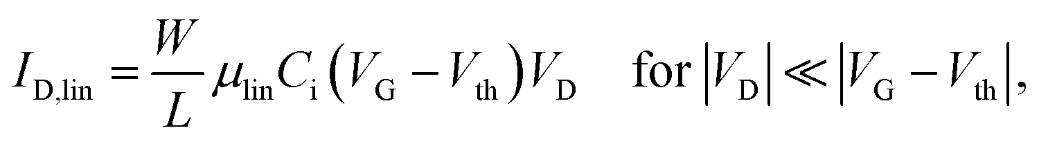 | (1) |
 | (2) |
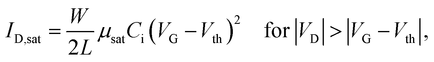
3.2. Thermionic emission
Understanding the internal energy barriers experienced by charge carriers has been a crucial part of interface engineering in OTFTs. One key aspect of the charge-carrier injection at the OSC–SD interface has been described through the following equation:48,49 | (3) |
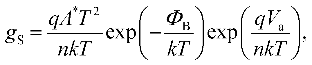 | (4) |
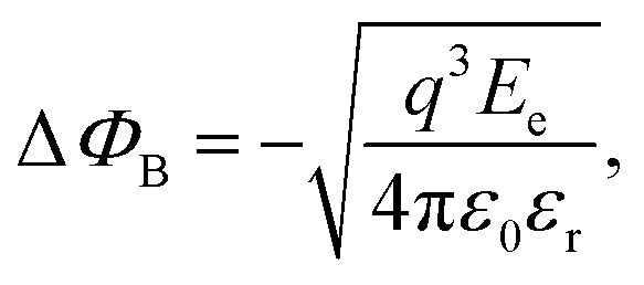 | (5) |
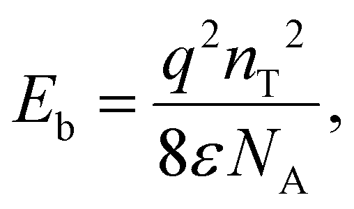
3.3. Grain boundary
Grain boundaries in polycrystalline OSCs, forming potential energy barriers, can interfere with charge carriers during the transport process. The Matthiessen's rule assumes that the effective mobility μeff in MOSFETs can be written as:52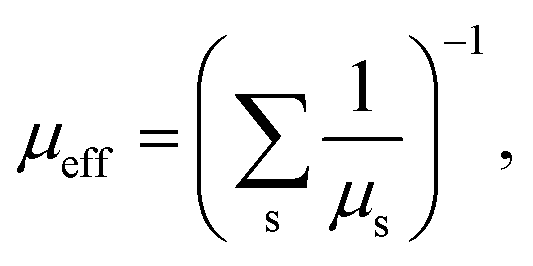 | (6) |
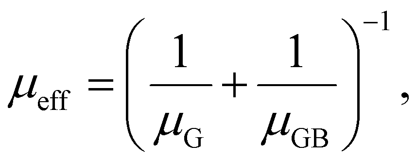 | (7) |
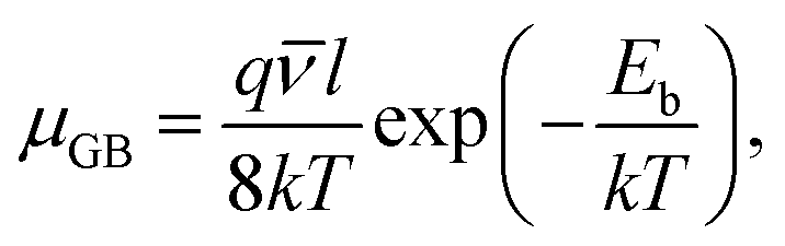 | (8) |
![[small nu, Greek, macron]](https://www.rsc.org/images/entities/i_char_e0ce.gif) is the electron thermal velocity, l is the length of a grain, and Eb is the barrier height at the grain boundary. eqn (8) indicates that the presence of grain boundaries with larger Ebs decreases the μGB, resulting in a lower μeff.
is the electron thermal velocity, l is the length of a grain, and Eb is the barrier height at the grain boundary. eqn (8) indicates that the presence of grain boundaries with larger Ebs decreases the μGB, resulting in a lower μeff.
The trapping of charge carriers at a grain boundary creates an energy barrier, the height of which can be estimated from:54
 | (9) |
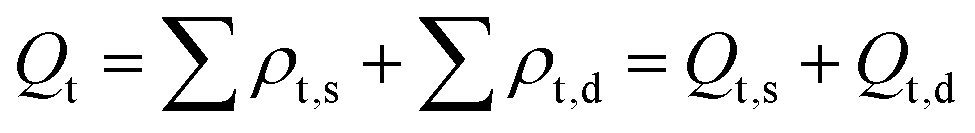
3.4. Trapped and free surface charges
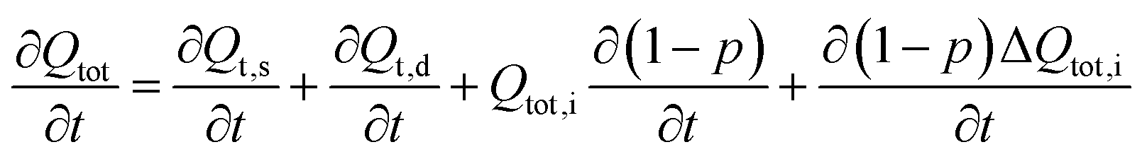
The total surface charge (Qtot) in TFTs, which can be divided into the trapped charge (Qt) and the free charge (Qf), is written as:57| Qtot = −Ci(VG − Vfb) = Qt + Qf, | (10) |
To reflect the trapping of charges followed by a reduction in Qf, and the variability of Qtot associated with external stimuli, eqn (10) is rewritten as:
| Qtot = Qt + Qf = Qt + (1 − p)(Qtot,i + ΔQtot,i) | (11) |
 .
.
Since the response of TFTs to various stimuli is a process accompanying the flow of time, it is useful to understand the temporal patterns of change in Qtot. eqn (11) indicates that Qtot, as a function of time t, has the following differential relationship:
 | (12) |
 | (13) |
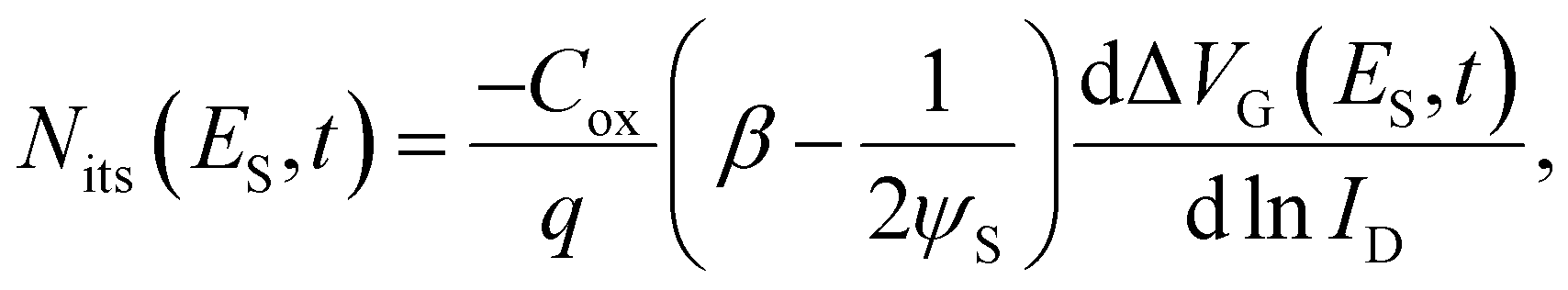
![[thin space (1/6-em)]](https://www.rsc.org/images/entities/char_2009.gif) ln(ID/k′), and ψS is the surface potential. The Nits formed in a field-effect device can exhibit a time-dependent variation involving thermal emission and tunneling processes,60 which is considered undesirable in the context of electrical stability.
ln(ID/k′), and ψS is the surface potential. The Nits formed in a field-effect device can exhibit a time-dependent variation involving thermal emission and tunneling processes,60 which is considered undesirable in the context of electrical stability.
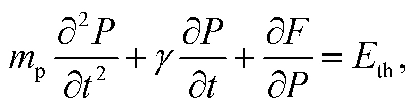
In addition, the Landau–Khalatnikov–Tani equation for ferroelectric domains with polarization fluctuations can be written as:63
 | (14) |
3.5. Charge transport mechanism
The multiple trapping and release (MTR) model has been frequently utilized to describe the charge-carrier transport in polycrystalline OSCs.49 In this model, the charge-carrier transport is assumed to occur through a transport band of extended states, with repeated trapping and thermal release processes through localized trap states under the band edge.65 The exponential energy distribution of localized trap states (Nt(E)), which is reflected in the MTR model, is generally expressed by: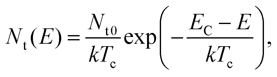 | (15) |
 | (16) |
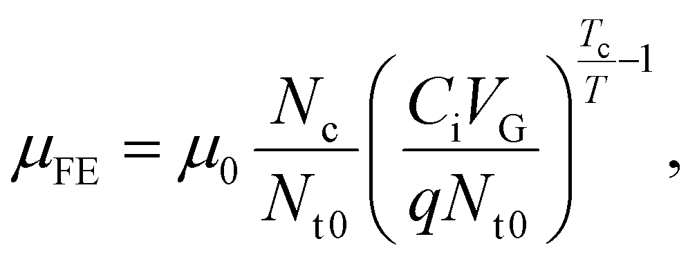
In addition, the variable-range hopping (VRH) model has been often used for highly disordered OSCs. In this model, hopping of charge carriers between localized states is considered to govern the charge-carrier transport. By combining the conductivity in percolation theory with an exponential energy distribution of localized states, the μFE is given as:67
 | (17) |
The MTR and VRH models may not fully describe the aspects of the temperature dependence of μFE. In these models, the Fermi–Dirac distribution is applied to each transport system for quantifying/estimating the filling of localized states. However, when external stimuli such as potential gradients are given to the systems, the charge carriers occupying localized states beneath the mobility edge (or beneath a specific transport energy) are likely to follow an emission-like dynamic process, which depends on temperature as well as the trap energy level. The carrier occupation of localized states defined by the Fermi–Dirac distribution is considered incompatible with the emission-like process that can perturb the equilibrium condition.
4. Characterization methods
4.1. Atomic force microscopy
Atomic force microscopy is a powerful imaging technique employed to visualize and characterize the surface morphological properties of materials.68 The electrical characteristics of OTFTs are greatly impacted by the surface morphological properties of the constituent material films, such as grain size, grain boundary density, surface roughness, wetting state, and various structural defects. Note that the interface between materials is simply a direct contact between their surfaces at a structural level. Atomic force microscopy, which is frequently utilized in OTFT research, has played a critical role in quantifying or investigating the correlations between the device characteristics and the surface morphological properties of the materials.694.2. X-Ray diffraction analysis
X-Ray diffraction is a powerful tool for studying the crystalline properties of materials.70 Through the analysis of the obtained X-ray diffraction patterns, it is possible to obtain information such as crystallinity, phase composition/purity, lattice parameters, and atomic/molecular arrangements. X-Ray diffraction is also one of the most frequently utilized analytical techniques in OTFT research, as their electrical characteristics are intimately associated with the crystalline properties of the materials.71 In particular, the growth of polycrystalline OSC films and their crystalline properties are significantly influenced by the external factors and process conditions, including substrate properties and ambient temperature. Accordingly, X-ray diffraction analysis has been highly instrumental in the development and optimization of OTFT technologies.4.3. Sum frequency generation spectroscopy
Sum frequency generation spectroscopy is a second-order non-linear optical technique that can yield the vibrational spectra of molecules at an interface.72,73 The analysis of the vibrational spectra provides information on the molecular conformation, orientation, and disorder at the interface. Investigating structural properties is one of the important tasks in OTFT research. The electrical characteristics of OTFTs are closely correlated with structural properties of the constituent interfaces at the molecular level.74–76 Hence, sum frequency generation spectroscopy is considered one of the necessary tools for the progress of OTFT technology.5. Diverse streams of interface engineering
5.1. The purposes of interface engineering in conventional OTFTs
In this text, the term 'conventional OTFTs' refers to the use of OTFTs as a driving element for active-matrix displays, or as a logic-circuit element for radio-frequency identification tags. Interface engineering has played a crucial role for improving the electrical performance and stability of OTFTs. Especially, interface engineering for conventional OTFTs has been evolving to minimize trap states and energy barriers that can interfere with the transport or injection of charge carriers. | ||
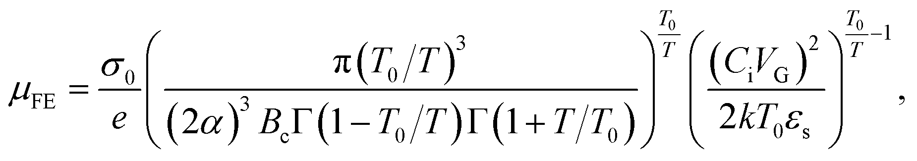
| Fig. 1 (a) The optical microscopy of the parallel (top) and perpendicular (bottom) OTFTs with the aligned PDI8-CN2 thin films, (b) the Arrhenius plots of the temperature-dependent mobilities for the OTFTs, with the blue symbols for the parallel devices and the red symbols for the perpendicular devices, and (c) the schematic diagrams of the proposed grain boundary types in the aligned PDI8-CN2 thin films. Reproduced from ref. 79 with permission from [Nature Portfolio], copyright [2009]. (d) The schematic diagram of the solution-shearing techniques based on a micropillar blade and (e) the X-ray phi-scan analysis of the reference and single-crystalline TIPS-pentacene thin films. Reproduced from ref. 83 with permission from [Nature Portfolio], copyright [2013]. | ||
Since grain boundaries in polycrystalline OSC thin films can act as charge traps and energy barriers,56,80 it has been essential to develop techniques for controlling the grain-boundary orientation and the molecular alignment feature at the grain boundaries. Various types of driving forces, such as centrifugal forces, electromagnetic waves, thermal gradients, and static magnetic fields, have been used to improve molecular alignment properties in OTFTs.29,30,42,81,82
Diao et al. reported an effective solution-shearing technology for fabricating thin films of 6,13-bis(triisopropylsilylethynyl)pentacene (TIPS-pentacene) with aligned single-crystalline domains.83 A shearing blade with crescent-shaped patterned micropillars were manufactured (Fig. 1d). The TIPS-pentacene thin film fabricated with the micropillar-patterned region in the blade exhibited a clear reduction in the grain-boundary density, compared to those fabricated with the non-patterned region in the blade. Furthermore, the researchers patterned wetting regions with an asymmetric triangle shape on a substrate in order to control the nucleation of crystalline domains. By combining the methods for controlling the nucleation and growth of crystalline domains, it was possible to achieve the formation of large-area single-crystalline domains in TIPS-pentacene thin films. The aligned TIPS-pentacene thin film with both the controlled nucleation and growth exhibited significantly enhanced crystalline quality, as indicated by the cross-polarized microscopy of the single-crystalline domains. X-Ray phi-scan analyses were performed on the TIPS-pentacene thin films to assess the crystalline quality. The aligned film displayed a relatively small angular spread of 3° in its diffraction pattern, while the reference film had a relatively large value of 60° (Fig. 1e). This confirmed high molecular alignment quality in the single-crystalline domains of the aligned film. OTFTs with the aligned TIPS-pentacene films were fabricated and their electrical characteristics were analyzed. This study demonstrated a useful technical route for large-area printed electronics.
 | (18) |
Minari et al. reported a technique for reducing the contact resistance based on the chemical doping of the OSC–SD interface.89 Dioctylbenzothienobenzothiophene (C8-BTBT) OTFTs were fabricated and explored (Fig. 2a). Prior to the formation of SD electrodes, iron(III)trichloride (FeCl3), which is known to be an acceptor material, was slightly evaporated as a dopant onto the C8-BTBT layer. In the electrical tests, the C8-BTBT OTFT with the FeCl3 doping was found to have electrical performance superior to a reference device without the FeCl3 doping (Fig. 2b). The contact resistance of the devices was extracted by using the transmission line method, which assumes the equation:
 | (19) |
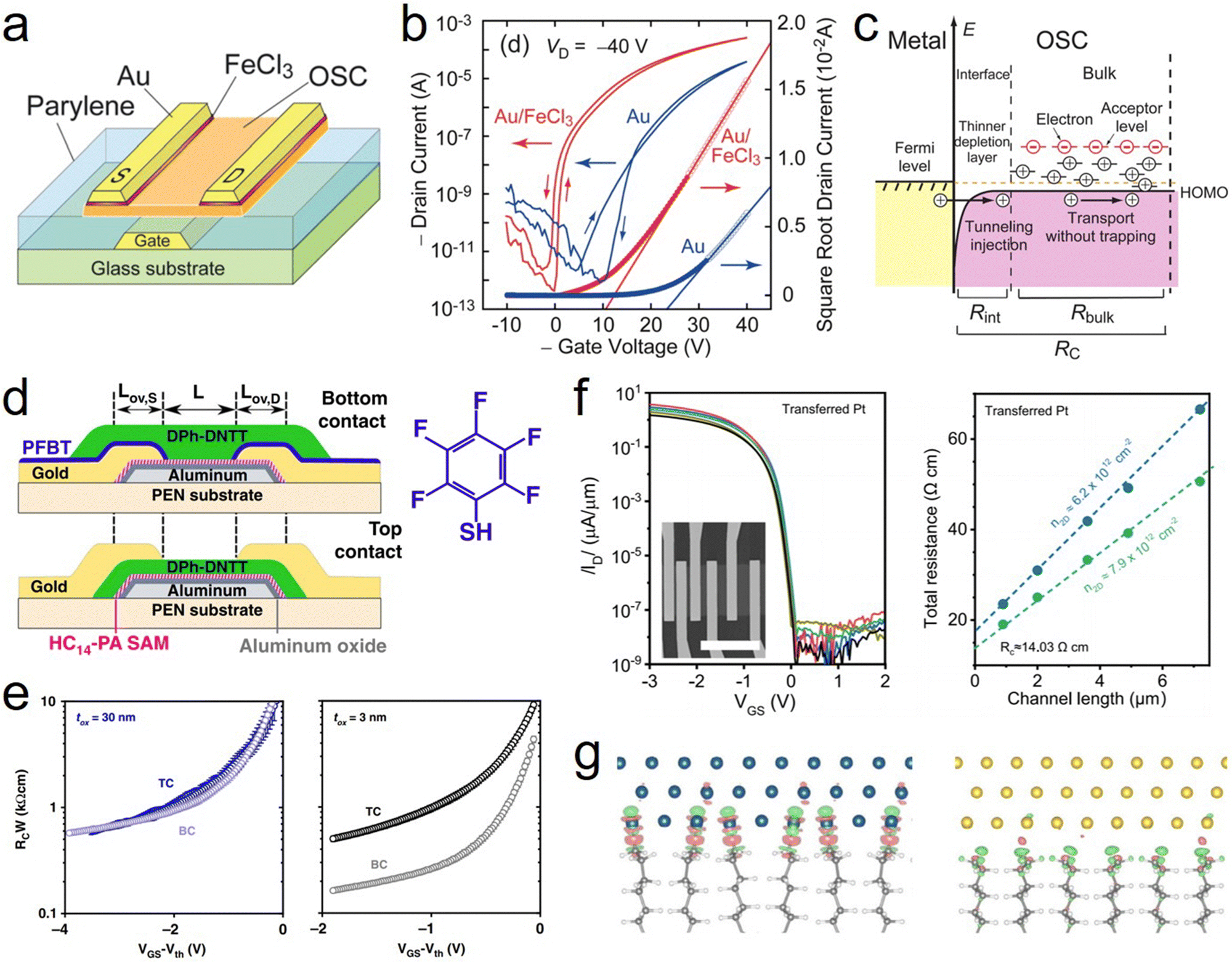 | ||
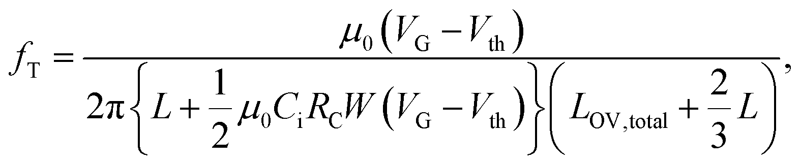
| Fig. 2 (a) The schematic diagram of the C8-BTBT OTFTs, (b) the transfer characteristic curves of the device with and without the contact doping, and (c) the energy diagram for a reduction in the Schottky-barrier thickness and the filling of trap states in the bulk region through the contact doping. Reproduced from ref. 89 with permission from [AIP Publishing], copyright [2012]. (d) The schematic diagram of the DPh-DNTT OTFTs, (e) the influence of the gate-insulator thickness on the gate-voltage-dependent contact resistance in the device. Reproduced from ref. 91 with permission from [Nature Portfolio], copyright [2019]. (f) The transfer characteristic curves of the transferred-Pt OTFTs with different channel lengths (left) and the corresponding contact-resistance extraction through the transmission line method (right) and (g) the differential charge density at the interfaces between C10-DNTT and Pt (left) and between C10-DNTT and Au (right) electrodes. Reproduced from ref. 9 with permission from [Nature Portfolio], copyright [2023]. | ||
The contact resistance is known to limit the transit frequency of OTFTs as well. The dependence of the transit frequency fT on the contact resistance can be expressed as:90
 | (20) |
Multifaceted efforts have intensely been made to reduce the contact resistance of OTFTs.92,93 Zeng et al. reported an effective approach to significantly reduce the contact resistance based on an electrode-transfer technique assisted by orbital hybridization.9 C10-DNTT OTFTs with transferred Pt SD electrodes were fabricated and explored (Fig. 2f). The transferred-Pt SD C10-DNTT OTFT exhibited the highest current density than those with transferred Au and evaporated Au SD electrodes. The highest current density was attributed to the best contact property between them. A significantly low contact resistance of 14.0 Ω cm was obtained for the transferred-Pt C10-DNTT OTFT (Fig. 2f). Moreover, the transferred-Pt C10-DNTT OTFT possessed improved electrical characteristics in the context of subthreshold swing, ON/OFF ratio, mobility, and Vth. Through density functional theory calculations, it was found that Pt has higher DOS near the HOMO states of C10-DNTT compared to Au. Accordingly, the contact-resistance reduction was attributed to the increased probability of tunneling at the OSC–SD interface. In addition, the Pt-catalyzed dehydrogenation of side alkyl chains, leading to the formation of Pt–C covalent bonds, was considered to promote orbital hybridization at the Pt–OSC interface and reduce the contact resistance, in contrast to the van der Waals gap formed at the Au–OS interface (Fig. 2g). A diode-connected transistor rectifier was successfully implemented using the transferred-Pt C10-DNTT OTFT. The significance of this study lies in proving a new and effective route for improving the contact resistance in OTFTs, aiming to achieve a leap in their electrical performance.
As various intrinsic and extrinsic factors induce electrical instability in OTFTs, it has been essential to address the electrical instability issue through multidimensional approaches based on interface engineering. Bulgarevich et al. developed pBTTT-C16 OTFTs with improved electrical stability using the hydroxyl-free fluoropolymer, CYTOP terminated with amidosilyl functional groups.96 They achieved patterning of the CYTOP layers on a silicon dioxide substrate through vacuum ultraviolet (UV) light exposure followed by a development process (Fig. 3a). The CYTOP-treated pBTTT-C16 OTFT exhibited smaller subthreshold swing and reduced current hysteresis than the octadecyltrichlorosilane (ODTS)-treated device. The subthreshold swing improvement and hysteresis suppression in the CYTOP-treated device, implying a reduction in the interfacial trap density, were attributed to an increased quality of the OSC–GI interface. Especially, the electrical stability tests revealed that the electrical stability of the CYTOP-treated pBTTT-C16 OTFT under gate bias stress in vacuum was significantly improved compared to the ODTS-treated device (Fig. 3b). The Vth stability of the devices was analyzed using the equation:
 | (21) |
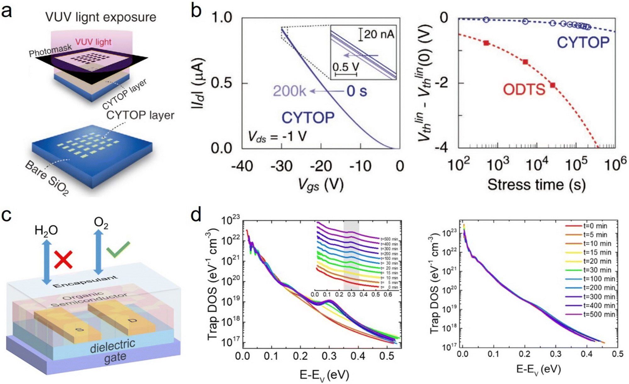 | ||
| Fig. 3 (a) The process for fabricating the hydrophobic–hydrophilic patterns on a substrate and (b) the transfer characteristic curves of the CYTOP-incorporated OTFTs obtained with the different bias stress times under vacuum conditions (left) and the threshold-voltage variations of the CYTOP- and ODTS-incorporated OTFTs according to the stress time (right). Reproduced from ref. 96 with permission from [Wiley], copyright [2020]. (c) The schematic diagram of the OTFT device encapsulated with the parylene N and (d) the trap density of states spectra obtained at different times during the device operation for the non-encapsulated (left) and encapsulated (right) devices. Reproduced from ref. 97 with permission from [Nature Portfolio], copyright [2021]. | ||
Considering extrinsic factors that can cause detrimental effects on the OSC–GI interface is also crucial for addressing the electrical instability issue of OTFTs. Iqbal et al. proposed an effective methodology for improving the electrical stability of OTFTs based on a sophisticated encapsulation technique.97 TnHS BDT trimer OTFTs encapsulated with parylene N were fabricated and explored (Fig. 3c). In particular, they carried out analyses for the trap DOS in the OSC bandgap utilizing the following equation:97
 | (22) |
5.2. The purposes of interface engineering in memory OTFTs
Attaining clear and stable data states is one of the key aspects in the development of memory OTFTs. Accordingly, the technological evolution of memory OTFTs has spanned various interface engineering for realizing and improving the non-equilibrium stability of each data state through sophisticated utilization of physical factors, e.g., electric dipoles and charge traps, sensitive to external conditions or stimuli. Ensuring the reversibility of data states is also one of the basic concerns in interface engineering for memory OTFTs.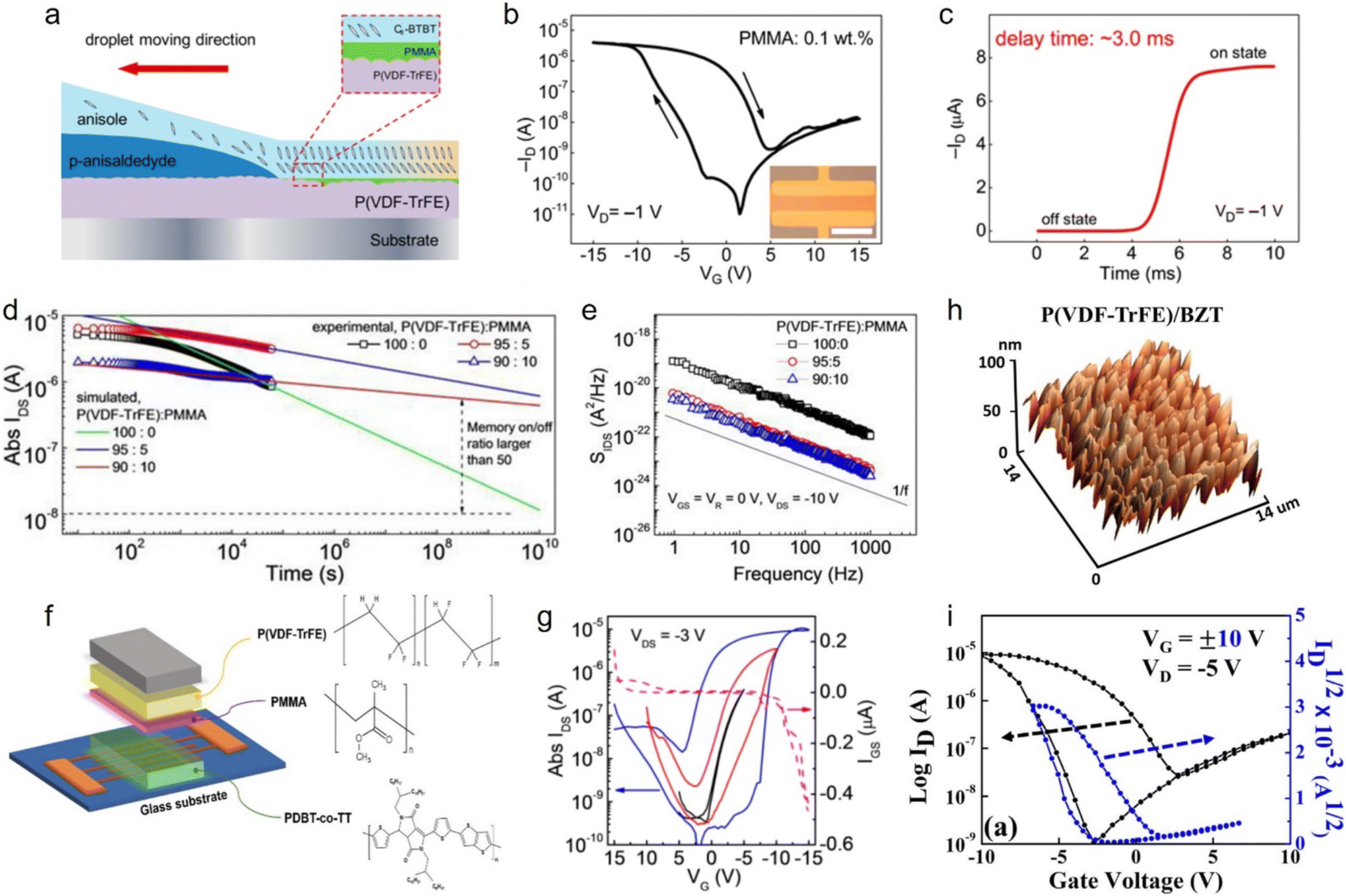 | ||
| Fig. 4 (a) The solution processing of the C8-BTBT thin film on the P(VDF-TrFE) thin film, with the PMMA-layer formation, (b) the transfer characteristics curves of the corresponding memory OTFT, and (c) the switching behaviour of the device. Reproduced from ref. 98 with permission from [The American Chemical Society], copyright [2017]. (d) The retention characteristics of the PMMA-incorporated memory OTFTs and the reference device and (e) the noise spectral densities of the corresponding devices. Reproduced from ref. 99 with permission from [AIP Publishing], copyright [2021]. (f) The schematic diagram of the memory OTFT and the chemical structure of the constituent materials and (g) the transfer characteristic curves of the device. Reproduced from ref. 100 with permission from [IEEE-Institute of Electrical and Electronics Engineers Inc.], copyright [2021]. (h) The atomic force microscopy image of the P(VDF-TrFE) thin film formed on the BZT thin film and (i) the transfer characteristic curves of the memory OTFT with the P(VDF-TrFE)/BZT hybrid GI. Reproduced from ref. 101 with permission from [IEEE-Institute of Electrical and Electronics Engineers Inc.], copyright [2022]. | ||
In the development of high-performance memory OTFTs, a thorough exploration on intrinsic factors that can affect the interfacial property has been required. Xu et al. reported a technology for achieving high-performance memory OTFTs through the self-organization of dielectric-combined ferroelectric GIs.99 They fabricated and explored PDBT-co-TT ferroelectric OTFTs with a top-gate structure. Blended PMMA/P(VDF-TrFE) GIs, obtained via phase separation, were incorporated as the GI. The phase separation method was chosen to avoid the solvent-induced damage of the PMMA buffer layer. The PDBT-co-TT memory OTFT exhibited a hysteresis behaviour in the transfer characteristic, where the 0 and 1 binary states are manifested. The device also exhibited an improved mobility of 1.96 cm2 Vs−1 compared to the device with a pure P(VDF-TrFE) GI. The presence of the PMMA buffer layer was considered to suppress the negative impacts of the polarization fluctuation and grain boundaries on the charge-transport property at the OSC-GI interface. Especially, the memory OTFT with the PMMA/P(VDF-TrFE) GI exhibited a significantly improved stable retention over 1.1 × 10⁴ s (Fig. 4d), as well as a reliable endurance property. Furthermore, the researchers carried out analyses on the low-frequency noise (Fig. 4e). The analyses revealed that the device with the PMMA/P(VDF-TrFE) GI had smaller noise spectral densities than the device with the pure P(VDF-TrFE) GI. Accordingly, the mobility improvement was attributed to reductions in the trap density and polarization fluctuation at the OSC-GI interface. This study provided a technological base for the development of high-performance memory OTFTs. Xu et al. also demonstrated a top-gate ferroelectric OTFT with low programming/erasing voltages (Fig. 4f).100 In their results, while the memory OTFT with a thin P(VDF-TrFE) failed to operate properly because of the large gate leakage, the device with a bilayer PMMA (55 nm)/P(VDF-TrFE) (155 nm) exhibited the suppressed leakage, memory ON/OFF ratio of 104, programming/erasing voltages of ±15 V, average mobility value of 1.01 cm2 V−1 s−1, and memory retention over 65000 s (Fig. 4g).
Charge-carrier transport in OTFTs is associated with dipole alignment properties at the OSC-GI interface. Yang et al. reported an improvement in the dipole alignment feature of a PMMA interlayer through controlling the adsorption process condition.75 The improved dipole alignment feature led to an increase in the mobility of an OTFT, which was attributed to a reduction in energy fluctuations at the OSC–GI interface.
Investigation on various materials and structures can be useful for preserving and maximizing the functionality of ferroelectric GIs. Lee et al. proposed a strategy for improving the thin film quality of P(VDF-TrFE) in memory OTFTs.101 Pentacene ferroelectric OTFTs with a P(VDF-TrFE) GI were fabricated and explored. They introduced a barium zirconate titanate (BZT) thin film as the bottom layer for the P(VDF-TrFE) GI in the bottom-gate top-contact device structure. The P(VDF-TrFE) thin film with the BZT bottom layer, i.e., the P(VDF-TrFE)/BZT hybrid thin film showed lower RMS surface roughness than a single P(VDF-TrFE) thin film (Fig. 4h). Specifically, the P(VDF-TrFE)/BZT hybrid thin film exhibited RMS surface roughness under 10 nm, while the single P(VDF-TrFE) thin film exhibited RMS surface roughness of 30 nm. The reduction in surface roughness of the P(VDF-TrFE) thin film was considered desirable for obtaining a better interfacial quality with the OSC layer, lower defect density, and suppressed leakage current. The memory OTFT with the P(VDF-TrFE)/BZT hybrid GI exhibited a large memory window of 7 V (Fig. 4i), with. Moreover, the device had a low operating voltage of ±10 V and a stable retention over 104 s. This study offers useful knowledge on the importance of morphological properties of ferroelectric GIs in memory OTFTs.
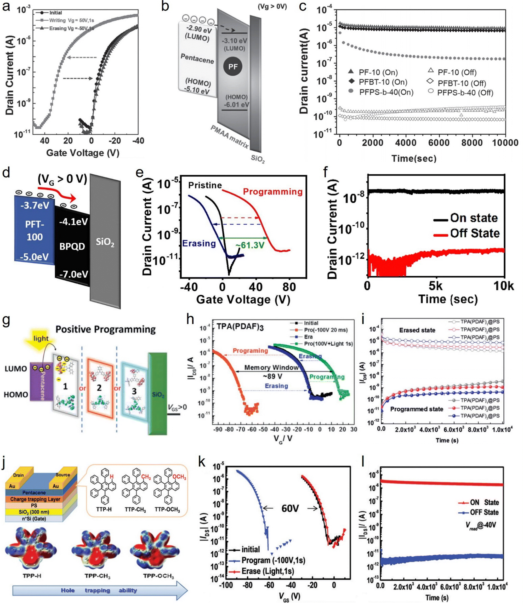 | ||
| Fig. 5 (a) The transfer characteristic curves of the memory OTFT with the polymeric nanoparticles, (b) the energy diagram of the proposed charge-trapping mechanism in the device, and (c) the retention characteristics of the memory OTFTs with the various electrets. Reproduced from ref. 102 with permission from [Wiley-VCH Verlag GmbH], copyright [2015]. (d) The energy diagram for the proposed memory mechanism in the memory OTFT with the BPQD, (e) the displacement of the transfer characteristic curve during the programming and erasing operations, and (f) the retention characteristic of the memory OTFT with a tunnelling layer. Reproduced from ref. 103 with permission from [IEEE-Institute of Electrical and Electronics Engineers Inc.], copyright [2020]. (g) The energy diagrams for the memory OTFT with the TPA(PDAF)n layers under positive gate voltages, (h) the transfer characteristic curves of the TPA(PDAF)3-based device during the programming and erasing processes, and (i) the retention characteristics of the optimized TPA(PDAF)3 device. Reproduced from ref. 104 with permission from [Wiley], copyright [2018]. (j) The schematic diagram of the memory OTFT, the chemical structures of TPP-H, TPP-CH3, and TPP-OCH3 molecules, and the 3D molecular electrostatic potential contour map of TPP-H, TPP-CH3, and TPP-OCH3 molecules, (k) the transfer characteristic curves of the device with the TPP-OCH3/polystyrene nanoarray after programming and erasing operations, and (l) the retention characteristic of the device. Reproduced from ref. 105 with permission from [The Royal Society of Chemistry], copyright [2022]. | ||
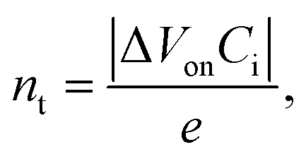
Researchers have adopted various materials and structures thereof to enhance the charge-storage capability in memory devices. Kumari et al. demonstrated a nano-floating-gate memory OTFT using black phosphorus quantum dots (BPQD) as the charge-trapping medium.103 They fabricated and explored nano-floating-gate memory OTFTs with a PFT-100 active layer. A positive gate pulse led to a positive shift of the transfer characteristic curve by the mechanism shown in Fig. 5d. The memory OTFT with the BPQDs exhibited ON/OFF current ratio of 1.3 × 10⁶ and a memory window of 61.3 V in the programming and erasing processes (Fig. 5e), as well as a good endurance property. The charge-trap density nt in the BPQD-based memory OTFT was calculated using the following equation:
 | (23) |
The design and synthesis of effective molecules specialized in the charge-trapping capability are one of the essential approaches for achieving high-performance memory OTFTs. Yu et al. demonstrated memory OTFTs based on the incorporation of 4,5-diazafluorene-based donor–acceptor small molecules.104 They fabricated and explored memory OTFTs with a pentacene active layer. TPA(PDAF)n (n = 1, 2, 3) were synthesized and utilized as the charge-trapping elements for the memory OTFTs. The TPA(PDAF)n (n = 1, 2, 3) devices exhibited sufficiently high ON/OFF current ratios of 5.1 × 10⁴, 11.1 × 10⁵, and 3.96 × 10⁴, respectively. Under the negative gate bias (programming), the devices displayed multibit memory windows with a negative Vth shift. The transferred holes were considered to be trapped by the triphenylamine moiety, causing the negative Vth shift. Moreover, in the light-assisted erasing process, the trapped holes were considered to be neutralized by the photo-induced electrons. Under the positive gate bias (light-assisted programming), the TPA(PDAF)3 device exhibited the largest positive memory window, which was attributed to its lowest LUMO level followed by an increase in the electron transfer from the pentacene layer (Fig. 5g). The transferred electrons were considered to be trapped by the 4,5-diazafluorene moiety. The TPA(PDAF)n (n = 1, 2, 3) devices had total memory windows of 52, 66, and 89 V, respectively (Fig. 5h). The researchers optimized their memory devices using a polystyrene charge-blocking layer. In the retention tests of the optimized devices, the TPA(PDAF)3 device exhibited an improved retention property over 104 s with ON/OFF current ratio of over ∼104 level (Fig. 5i). This study offers a useful guideline for achieving high storage capacity in memory OTFTs in terms of material design and selection.
Yang et al. developed memory OTFTs using wide-bandgap polyphenyl substituted naphthalene-based compounds (TPPs) as the charge-trapping materials.105 Pentacene OTFTs with pure TPP-H, TPP-CH3, and TPP-OCH3 layers, as well as the device with the TPP-OCH3/polystyrene nanoarray, were fabricated and explored (Fig. 5j). The memory windows of the devices with the pure TPP-OCH3, TPP-CH3, and TPP-H layers were 50, 40, and 33 V, respectively. The relatively small HOMO mismatch between TPP-OCH3 and pentacene, as well as the larger dipole moment and more negative electrostatic potential of TPP-OCH3 (Fig. 5j), was considered to enhance the hole trapping and result in the largest memory window of the device. Furthermore, the researchers adopted the TPP-OCH3/polystyrene nanoarray for better device stability and storage capacity. The nanoarray device exhibited a large memory window of 60 V (Fig. 5k), while that of the pure TPP-OCH3 device was 48 V. For the nanoarray device, the programming operation was performed with the VG of −100 V, and the erasing operation was performed with light illumination. Compared to the pure-TPP-OCH3 device, the nanoarray device exhibited a significantly improved memory retention over 104, with the current ON/OFF ratio of 2.8 × 10⁵ (Fig. 5l). The improvements in the memory capacity and stability were attributed to the isolated nanoarray structures and the generation of an interfacial dipole at the pentacene/nanoarray interface. This study provides useful knowledge for enhancing the performance and stability of memory OTFTs in terms of material design and structural optimization.
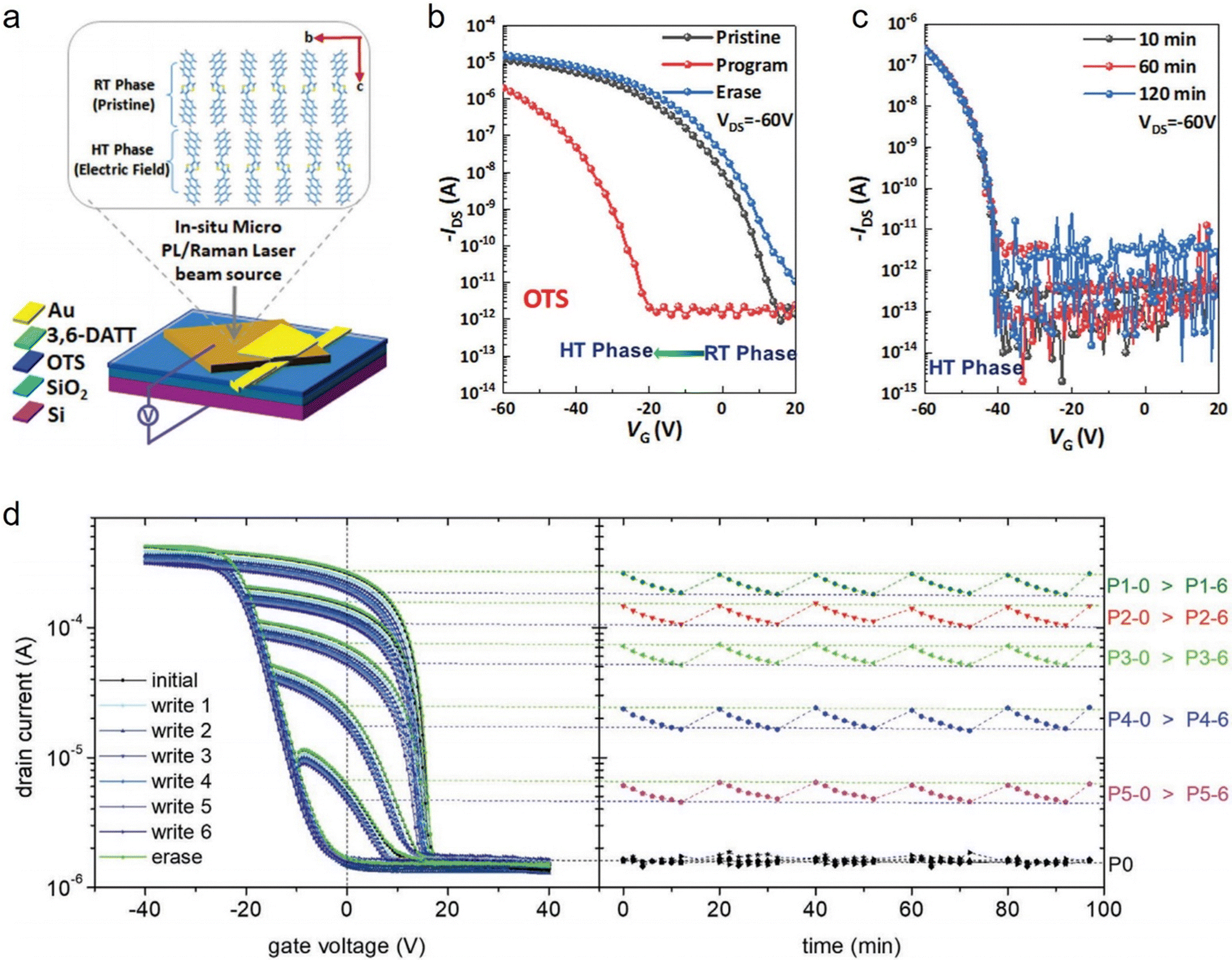 | ||
| Fig. 6 (a) The schematic diagrams of the memory OTFT and the RT and HT phases of the 3,6-DATT crystals, (b) the transfer characteristic curves of the device after programming and erasing operations, and (c) the retention characteristic of the device. Reproduced from ref. 106 with permission from [Wiley], copyright [2023]. (d) The light modulation of the transfer characteristic of the photochromic-ferroelectric OTFT for the different ferroelectric polarization states. Reproduced from ref. 107 with permission from [Wiley-VCH Verlag GmbH], copyright [2021]. | ||
Carroli et al. developed a multilevel memory technique based on a photochromic-ferroelectric OTFT with 11 bit storage capacity.107 The researchers fabricated ferroelectric OTFTs with a P(VDF-TrFE) GI and bi-component P3HT/DAE-Me active layer, and analyzed their electrical characteristics. The partial polarization feature of the P(VDF-TrFE) GI allowed for the formation of five distinct current levels in the device. In particular, the open state of the DAE-Me molecules, obtained through UV-light exposure, was used to decrease the device current, while the closed state of the DAE-Me molecules, obtained through green-light exposure, was used to increase the device current back to its initial level. By utilizing the photo-isomerization of the DAE-Me molecules, more than 500 distinct current levels were achieved for each of the five ferroelectric polarization states, thereby yielding 2500 levels in total (>11 bit). As shown in Fig. 6d, they demonstrated the multilevel operation of the device, where the intermediate states for each base level were obtained through UV-light exposure and the erase operation was performed by green-light exposure. This study proposes a technological route for implementing the multilevel operation and provides useful insights into addressing the growing demand for data storage.
5.3. The purposes of interface engineering in sensor OTFTs
Interface engineering has led the progress of sensor OTFT technology, especially in the context of the sensitivity and selectivity properties. Interface engineering has played an essential role for maximizing the efficiency of interactions between the active layer and target analytes, thereby improving the sensitivity. Moreover, implementing functional surfaces for the selective detection of target analytes has been an appealing role of interface engineering for sensor OTFTs as well.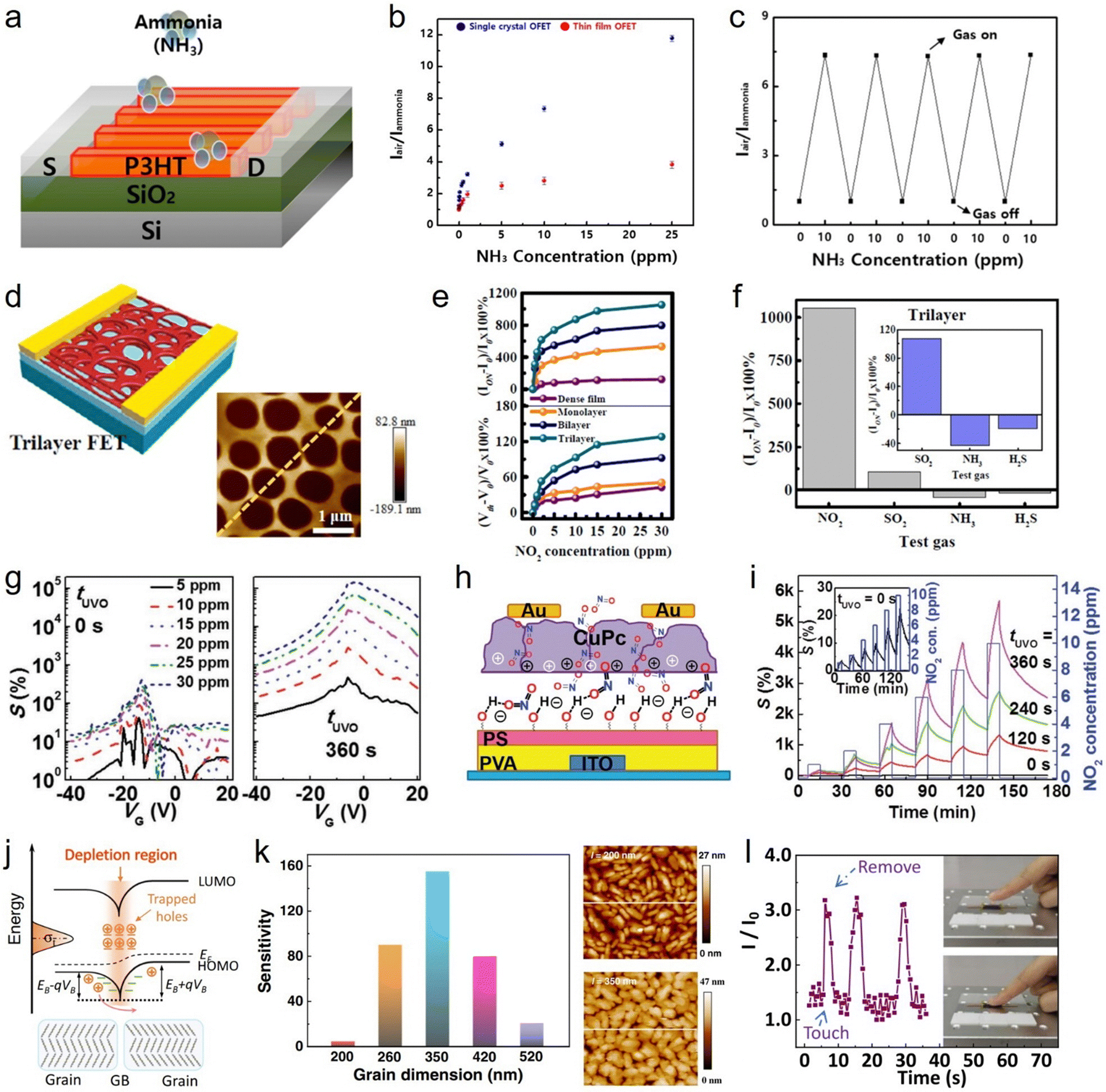 | ||
| Fig. 7 (a) The schematic diagram of the interaction between the nanowire sensor OTFT and ammonia molecules, (b) the current variations of the nanowire and reference devices under exposure to ammonia, and (c) the repeatability test of the devices. Reproduced from ref. 109 with permission from [The American Chemical Society], copyright [2017]. (d) The schematic diagram of the porous sensor OTFT (left) and the atomic force microscopy of the active layer surface (right), (e) the variations in the ON current and Vth under exposure to different nitrogen dioxide concentrations, and (f) the selectivity of the trilayer device with different gas species. Reproduced from ref. 110 with permission from [Elsevier Science SA], copyright [2022]. (g) The sensitivity of the UVO-treated sensor OTFT and the reference device for different nitrogen dioxide concentrations, (h) the proposed mechanism for the nitrogen dioxide sensing of the device, and (i) the real-time sensitivity of the device. Reproduced from ref. 111 with permission from [Wiley-VCH Verlag GmbH], copyright [2017]. (j) The grain boundary model for polycrystalline semiconductors with a bias voltage, (k) (left) the variation in the sensitivity of the sensor OTFT according to the grain size and (right) the atomic force microscopy image of the DNTT film with the grain sizes of 200 and 350 nm, and (l) the response of the sensor OTFT to finger tough. Reproduced from ref. 56 with permission from [Nature Portfolio], copyright [2021]. | ||
Exploring diverse morphologies in sensor OTFTs has been required for enhancing their sensing performance. Gao et al. developed a sensor OTFT with remarkably high sensitivity to NO2 based on a multilayer porous structure.110 They fabricated a multilayer porous P3HT film, which was used as the active layer of the sensor OTFT (Fig. 7d). When the multilayer porous OTFTs were exposed to NO2, the ON current (ION) increased and the Vth shifted in the positive direction with increasing the NO2 concentration. Specifically, the trilayer porous OTFT exhibited the greatly enhanced ION responsivity of 1053%, while a reference device with a dense P3HT film exhibited the ION responsivity of 122% (Fig. 7e). The Vth responsivity of the trilayer porous OTFT was 128%, while that of the reference device was 42% (Fig. 7e). In particular, the sensitivity calculations revealed that the trilayer porous OTFT had higher sensitivity than the bilayer and monolayer porous OTFTs. For the trilayer device, the increased adsorption sites and continuous diffusion pathways were considered to facilitate the analyte-induced generation of charge carriers. Furthermore, the researchers investigated the selectivity of the multilayer porous OTFTs. For comparison, the trilayer OTFT was exposed to one oxidizing gas, i.e., SO2 and two reducing gases, i.e., NH3 and H2S. Consequently, the device demonstrated higher sensitivity to NO2 compared to the other examined gases (Fig. 7f). It was also noted that the sensors can operate under high humidity conditions of 70% RH at room temperature. This study provides a useful technological foundation for designing the morphology of the active layer in OTFTs.
Not only structural approaches but also chemical modulation of the constituent layers can offer an effective route to enhance the sensing performance of OTFTs. Huang et al. developed a sensor OTFT technique for highly sensitive detection of NO2 based on interfacial modification.111 Sensor OTFTs with a CuPc active layer were fabricated and explored. They performed an UV-ozone (UVO) treatment on the polystyrene layer of the GI. The UVO-treated device exhibited significantly enhanced NO2 sensitivity compared to a reference device without UVO treatment (Fig. 7g). When the NO2 concentration increased, significantly larger variations in the ON current and turn-on voltage were observed for the UVO-treated device. The morphological analyses on the OSC and GI revealed no significant correlation between their morphologies and the enhanced sensitivity. Oxygenated polar functionalities on the UVO-treated polystyrene surface were considered to physically adsorb NO2 molecules, followed by the polarization effect-induced positive charge generation in the OSC layer (Fig. 7h). X-ray photoelectron spectroscopy and Fourier transform infrared spectroscopy were performed on the polystyrene surfaces. The chemical analyses on the UVO-treated polystyrene layer revealed the formation of new polar groups on the polystyrene surface and the possibility of physical adsorption of NO2 molecules. Furthermore, the real-time sensitivity tests showed that the sensitivity of the UVO-treated device for various NO2 concentrations greatly increased with increasing the time of UVO treatment on the polystyrene layer (Fig. 7i). These results indicate that modulating the chemical properties of the OSC–GI interface can lead to a significant increase in the sensing performance.
Huang et al. demonstrated an effective sensor OTFT for detecting temperature through potential barrier engineering.56 They fabricated OTFTs with DNTT as the active layer material. The potential barrier engineering for implementing the temperature sensor was performed based on the following equation:56
 | (24) |
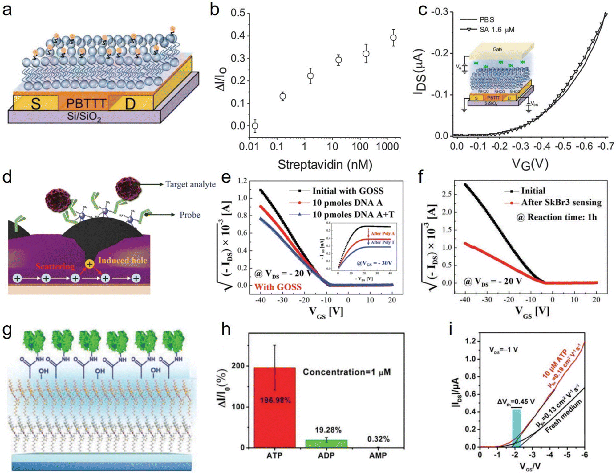 | ||
| Fig. 8 (a) The schematic diagram of the sensor OTFT with the anchored biotinylated phospholipids, (b) the current variations of the sensor OTFT under exposure to the different streptavidin concentration, and (c) the response of the device with the phospholipid layer without biotin to streptavidin. Reproduced from ref. 112 with permission from [The Royal Society of Chemistry], copyright [2015]. (d) The proposed sensing mechanism of the sensor OTFT with the graphene oxide, (e) the variation in the transfer characteristic curve of the device by the immobilization of poly-A DNA, and by the hybridization of poly-T DNA, and (f) the variation in the transfer characteristic curve by the SkBr3 attachment. Reproduced from ref. 113 with permission from [The Royal Society of Chemistry], copyright [2017]. (g) The schematic diagram of the formed enzyme-containing molecular antennas on the active layer in the sensor OTFT, (h) the selectivity tests of the device with various analytes, and (i) the variations in the Vth and mobility of the device under exposure to adenosine triphosphate. Reproduced from ref. 114 with permission from [The Royal Society of Chemistry], copyright [2018]. | ||
Finding and investigating the sensing functionality of various recognition elements in sensor OTFTs has been instrumental in the realization of specific analyte detection. Lee et al. proposed a sensor OTFT technology for the selective detection of DNA and circulating tumor cells (CTC).113 Sensor OTFTs with a pentacene active layer were fabricated and explored. In particular, they formed a functionalized graphene oxide (GO) layer with on the pentacene active layer (Fig. 8d). It was mentioned that the GO seeped into the pentacene grain boundaries and formed π–π bonding. The devices with and without the GO layer exhibited a comparable charge transport property. The reference device without the GO layer displayed no significant variation in the mobility by the exposure to DNA molecules. In contrast, the mobility of the GO-incorporated device decreased after the immobilization of poly-A DNA; specifically from 0.097 to 0.063 cm2 V−1 s−1 (Fig. 8e). Moreover, after the hybridization of poly-T DNA, the mobility further decreased to 0.044 cm2 V−1 s−1 (Fig. 8e). The negative charge on the DNA molecules was considered to attract holes at the pentacene grain boundaries, thereby hindering the charge transport at the OSC–GI interface. In addition, the GO-incorporated device also exhibited lowered mobility when exposed to SkBr3 CTC; specifically the SkBr3 attachment led to a significant 95% reduction in the mobility (Fig. 8f). Through the fluorescence image analyses, the researchers confirmed the antigen–antibody interaction using the SkBr3 cells. This study contributed to confirming the effectiveness of the use of proper recognition elements in the selective detection of target analytes.
The progress of sensor OTFT technology has been accompanied by the development of sophisticated surface modulation techniques. Shen et al. suggested a sensor OTFT for the selective adenosine triphosphate (ATP) detection based on a molecular antenna.114 Sensor OTFTs with a PDPP3T active layer were fabricated and explored. Especially, they incorporated enzyme-containing molecular antennas on the surface of the active layer (Fig. 8g). The process for fabricating the molecular antennas included the formation of surface binding groups. In the electrical tests under exposure to ATP, the current of the molecular antenna device increased with the increasing ATP concentration. The detection limit was found to be 0.1 nM. The device exhibited a good reproducibility property as well. Furthermore, the researchers investigated the selectivity using other materials, i.e., adenosine diphosphate (ADP) and adenosine monophosphate (AMP) (Fig. 8h). The molecular antenna device exhibited a large variation in the current (196.98%), while under exposure to the ADP and AMP (Fig. 8h), exhibiting only 19.28% and 0.32% variations, respectively. They observed a reduction in the Vth magnitude, i.e., 0.45 V and an increase in the mobility, i.e., from 0.13 to 0.19 cm2 V−1 s−1 (Fig. 8i). Accordingly, the exposure to ATM was considered to result in variations in the concentration of charge carrier and the mobility. This study provided an effective technological guideline for implementing sensor OTFTs with high selectivity.
6. Summary and perspectives
This review underlined the diverse technological streams of interface engineering formed in the field of OTFTs. It was necessary to categorize the previous research based on the purposes and roles of interface engineering as follows: in Section 5, 5.1. The purposes of interface engineering in conventional OTFTs with ‘5.1.1. Suppression of molecular disorder’, ‘5.1.2. Enhancement of contact properties’, and ‘5.1.3. Inhibition of trap-state formation’, 5.2. The purposes of interface engineering in memory OTFTs with ‘5.2.1. Stabilization of non-equilibrium polarization’, ‘5.2.2. Enhancement of non-equilibrium charge trapping’, and ‘5.2.3. Exploitation of intramolecular responses’, and lastly, 5.3. The purposes of interface engineering in sensor OTFTs with ‘5.3.1. Enhancement of interaction efficiency’ and ‘5.3.2. Implementation of target recognition’. It is worth noting that the purpose and roles of interface engineering described in all these sections exhibit a deep interconnectedness on a physical level, while at the same time, there are distinct differences in the OTFT functionality pursued by interface engineering.Interestingly, interface engineering takes on different forms and characters depending on the specific functionality of OTFT applications. For example, one key aspect of interface engineering for conventional OTFTs has been suppressing interactions with the environment, while for sensor OTFTs, it has been specialized in exploiting interactions with the environmental elements in a sophisticated manner. Although OTFT devices consist solely of two primary interfaces, i.e., the OSC–GI and OSC–SD interfaces, the charge-carrier dynamics at these interfaces are dependent on multiple driving factors with complex causality and correlations. The categorization of interface engineering based on its purpose and role is believed to deepen our understanding of how variations in these complex factors can lead to subtle or dramatic changes in the device characteristics.
In the future, a more sophisticated form of interface engineering with accumulated knowledge will play a crucial role in the development of OTFT technology. The accumulated knowledge indicate both theoretical and experimental aspects. We consider that crossover of technologies and knowledge between different subfields will lead to emergence of new phenomena or functions, as well as the upgrade of existing OTFT technologies. The combination of various heterogeneous materials will possibly be one important aspect in the development of OTFT technology.35,115,116 The purpose and role of interface engineering in OTFTs are variable and dynamic. The attempts to endow certain functionality or better characteristics to OTFTs through interface engineering are actively ongoing even now. Through the development of individual techniques and their convergence, optimal or new forms of interface engineering can emerge at any time, leading to noteworthy progress in OTFT technology.
Conflicts of interest
The authors declare no conflict of interest.Acknowledgements
This work was supported by Basic Science Research Program through the National Research Foundation of Korea (NRF) funded by the Ministry of Education (2021R1A6A3A01088549), by Basic Science Research Program through the National Research Foundation of Korea (NRF) funded by the Ministry of Education (2018R1A6A1A03026005), and by the National Research Foundation of Korea (NRF) grant funded by the Korea government (MSIT) (2021R1A2C1011429).References
- U. Zschieschang and H. Klauk, J. Mater. Chem. C, 2019, 7, 5522–5533 RSC.
- H. Sirringhaus, Adv. Mater., 2014, 26, 1319–1335 CrossRef CAS PubMed.
- D. Braga and G. Horowitz, Adv. Mater., 2009, 21, 1473–1486 CrossRef CAS.
- A. Spanu, L. Martines and A. Bonfiglio, Lab Chip, 2021, 21, 795–820 RSC.
- W. Wang, Z. He, C. Di and D. Zhu, Mater. Today Electron., 2023, 3, 100028 CrossRef.
- T. Sekitani, U. Zschieschang, H. Klauk and T. Someya, Nat. Mater., 2010, 9, 1015–1022 CrossRef CAS PubMed.
- K. Liu, B. Ouyang, X. Guo, Y. Guo and Y. Liu, npj Flexible Electron., 2022, 6, 1 CrossRef CAS.
- C. Liao, M. Zhang, M. Y. Yao, T. Hua, L. Li and F. Yan, Adv. Mater., 2015, 27, 7493–7527 CrossRef CAS PubMed.
- J. Zeng, D. He, J. Qiao, Y. Li, L. Sun, W. Li, J. Xie, S. Gao, L. Pan, P. Wang, Y. Xu, Y. Li, H. Qiu, Y. Shi, J.-B. Xu, W. Ji and X. Wang, Nat. Commun., 2023, 14, 324 CrossRef CAS PubMed.
- B. Wang, T. Xu, B. Yu, J. Zou and S. Luan, ACS Appl. Mater. Interfaces, 2023, 15, 7204–7216 CrossRef CAS PubMed.
- N. Zhang, W. Li, J. Zhu, T. Wang, R. Zhang, K. Chi, Y. Liu, Y. Zhao and X. Lu, Adv. Mater., 2023, 35, 2300094 CrossRef CAS PubMed.
- Y. Bao, L. Zhang, H. Wei, B. Cao and T. Yang, Phys. Chem. Chem. Phys., 2023, 25, 15279–15286 RSC.
- S. Sun, J. Zhu, Z. Wang, Y. Huang, Y. Hu, X. Chen, Y. Sun, L. Li and W. Hu, Adv. Mater., 2023, 2306975 CrossRef PubMed.
- Y. Xiao, W. Deng, J. Hong, X. Ren, X. Zhang, J. Shi, F. Sheng, X. Zhang and J. Jie, Adv. Funct. Mater., 2023, 33, 2213788 CrossRef CAS.
- T. Shen, W. Li, Y. Zhao, Y. Wang and Y. Liu, Adv. Funct., 2023, 35, 2210093 CAS.
- B. Fu, F. Yang, L. Sun, Q. Zhao, D. Ji, Y. Sun, X. Zhang and W. Hu, Adv. Mater., 2022, 34, 2203330 CrossRef CAS PubMed.
- Y. Yang, H. Sun, X. Zhao, D. Xian, X. Han, B. Wang, S. Wang, M. Zhang, C. Zhang, X. Ye, Y. Ni, Y. Tong, Q. Tang and Y. Liu, Adv. Sci., 2022, 9, 2105125 CrossRef CAS PubMed.
- K. Takimiya, K. Bulgarevich, S. Horiuchi, A. Sato and K. Kawabata, ACS Mater. Lett., 2022, 4, 675–681 CrossRef CAS.
- M. Lee, B.-i Choi, P. Ahn, Y. Y. Choi, Y. Heo, J. Kim, J. H. Min, T. J. Shin, K. Kim, H. Choi, H. Kweon, D. H. Ho, J. I. Yoon, H. Kim, E. Lee, D. H. Kim, K. Kwak, M. S. Kang, J. H. Cho and B. S. Kim, Chem. Mater., 2022, 34, 10409–10423 CrossRef CAS.
- Y. Sui, Z. Wang, J. Bai, Y. Shi, X. Zhang, Y. Deng, Y. Han and Y. Geng, J. Mater. Chem. C, 2022, 10, 2616–2622 RSC.
- J. Guo, D. Liu, W. Li, B. Yu, H. Tian, F. Zhu and D. Yan, Org. Electron., 2021, 93, 106170 CrossRef CAS.
- Z. Wang, Y. Shi, Y. Deng, Y. Han and Y. Geng, Adv. Funct. Mater., 2021, 31, 2104881 CrossRef CAS.
- C. Liu, X. Liu, G. Zheng, X. Gong, C. Yang, H. Liu, L. Zhang, C. L. Anderson, B. He, L. Xie, R. Zheng, H. Liang, Q. Zhou, Z. Zhang, J. Chen and Y. Liu, J. Mater. Chem. A, 2021, 9, 23497–23505 RSC.
- X. Fang, J. Shi, X. Zhang, X. Ren, B. Lu, W. Deng, J. Jie and X. Zhang, Adv. Funct. Mater., 2021, 31, 2100237 CrossRef CAS.
- A. Velusamy, C. Yu, S. N. Afraj, C.-C. Lin, W.-Y. Lo, C.-J. Yeh, Y.-W. Wu, H.-C. Hsieh, J. Chen, G.-H. Lee, S.-H. Tung, C.-L. Liu, M.-C. Chen and A. Facchetti, Adv. Sci., 2021, 8, 2002930 CrossRef CAS PubMed.
- H. Ma, H.-L. Yip, F. Huang and A. K.-Y. Jen, Adv. Funct. Mater., 2010, 20, 1371–1388 CrossRef CAS.
- C. Di, Y. Liu, G. Yu and D. Zhu, Acc. Chem. Res., 2009, 42, 1573–1583 CrossRef CAS PubMed.
- D. Liu and Q. Miao, Mater. Chem. Front., 2018, 2, 11–21 RSC.
- J. Park, C.-M. Keum, J.-H. Kim, S.-D. Lee, M. Payne, M. Petty, J. E. Anthony and J.-H. Bae, Appl. Phys. Lett., 2013, 102, 013306 CrossRef.
- J.-H. Kwon, D.-K. Kim, J. Jang, J. Park, S.-W. Kang and J.-H. Bae, Org. Electron., 2017, 47, 44–50 CrossRef CAS.
- M.-H. Kim, S.-P. Noh, C.-M. Keum, J.-H. Bae and S.-D. Lee, Org. Electron., 2012, 13, 2365–2371 CrossRef CAS.
- J.-H. Bae, J. Park, C.-M. Keum, W.-H. Kim, M.-H. Kim, S.-O. Kim, S. K. Kwon and S.-D. Lee, Org. Electron., 2010, 11, 784–788 CrossRef CAS.
- J.-H. Kwon, J. Lee, M.-H. Kim, J.-H. Bae and J. Park, Org. Electron., 2021, 99, 106345 CrossRef CAS.
- J.-H. Bae, C. Jeong, S.-D. Lee and C.-J. Yu, Solid-State Electron., 2012, 68, 108–112 CrossRef CAS.
- M.-J. Kim, W.-S. Kim, C.-H. Kim, J.-H. Kwon and M.-H. Kim, J. Mater. Chem. C, 2023, 11, 12675–12684 RSC.
- Z. Feng, Z. Cheng, H. Jin and P. Lu, J. Mater. Chem. C, 2022, 10, 4497–4520 RSC.
- E. K. Solak and E. Irmak, RSC Adv., 2023, 13, 12244–12269 RSC.
- G. Giri, E. Verploegen, S. C. B. Mannsfeld, S. Atahan-Evrenk, D. H. Kim, S. Y. Lee, H. A. Becerril, A. Aspuru-Guzik, M. F. Toney and Z. Bao, Nature, 2011, 480, 504–508 CrossRef CAS PubMed.
- H.-R. Tseng, H. Phan, C. Luo, M. Wang, L. A. Perez, S. N. Patel, L. Ying, E. J. Kramer, T.-Q. Nguyen, G. C. Bazan and A. J. Heeger, Adv. Mater., 2014, 26, 2993–2998 CrossRef CAS PubMed.
- Y. Kim, S. Chung, K. Cho, D. Harkin, W.-T. Hwang, D. Yoo, J.-K. Kim, W. Lee, Y. Song, H. Ahn, Y. Hong, H. Sirringhaus, K. Kang and T. Lee, Adv. Mater., 2019, 31, 1806697 CrossRef PubMed.
- L. Xiang, W. Wang and W. Xie, Sci. Rep., 2016, 6, 36291 CrossRef CAS PubMed.
- C.-M. Keum, J.-H. Kwon, S.-D. Lee and J.-H. Bae, Solid-State Electron., 2013, 89, 189–193 CrossRef CAS.
- D. Kumaki, S. Ando, S. Shimono, Y. Yamashita, T. Umeda and S. Tokito, Appl. Phys. Lett., 2007, 90, 053506 CrossRef.
- G. Horowitz, J. Mater. Res., 2004, 19, 1946–1962 CrossRef CAS.
- T. Li, J. W. Balk, P. P. Ruden, I. H. Campbell and D. L. Smith, J. Appl. Phys., 2002, 91, 4312–4318 CrossRef CAS.
- A. Kumatani, Y. Li, P. Darmawan, T. Minari and K. Tsukagoshi, Sci. Rep., 2013, 3, 1026 CrossRef PubMed.
- H.-I. Un, J.-Y. Wang and J. Pei, Adv. Sci., 2019, 6, 1900375 CrossRef CAS PubMed.
- J. W. Borchert, R. T. Weitz, S. Ludwigs and H. Klauk, Adv. Mater., 2022, 34, 2104075 CrossRef CAS PubMed.
- C. Liu, K. Huang, W.-T. Park, M. Li, T. Yang, X. Liu, L. Liang, T. Minari and Y.-Y. Noh, Mater. Horiz., 2017, 4, 608–618 RSC.
- J.-H. Kwon, H. Lee, B. Kim, X. Zhang, J. Jang, J.-H. Bae and J. Park, Adv. Mater. Interfaces, 2021, 8, 2101104 CrossRef CAS.
- W. Wang, T. Lee and M. A. Reed, Phys. Rev. B: Condens. Matter Mater. Phys., 2003, 68, 035416 CrossRef.
- D. Esseni and F. Driuss, IEEE Trans. Electron Devices, 2011, 58, 2415–2422 CAS.
- G. Horowitz, M. E. Hajlaoui and R. Hajlaoui, J. Appl. Phys., 2000, 87, 4456–4463 CrossRef CAS.
- V. Rani, A. Sharma, P. Kumar, B. Singh and S. Ghosh, RSC Adv., 2017, 7, 54911–54919 RSC.
- Z. Chu, M. Yang, P. Schulz, D. Wu, X. Ma, E. Seifert, L. Sun, X. Li, K. Zhu and K. Lai, Nat. Commun., 2017, 8, 2230 CrossRef PubMed.
- Y. Huang, X. Gong, Y. Meng, Z. Wang, X. Chen, J. Li, D. Ji, Z. Wei, L. Li and W. Hu, Nat. Commun., 2021, 12, 21 CrossRef CAS PubMed.
- G. Horowitz and P. Delannoy, J. Appl. Phys., 1991, 70, 469–475 CrossRef CAS.
- H. F. Haneef, A. M. Zeidell and O. D. Jurchescu, J. Mater. Chem. C, 2020, 8, 759–787 RSC.
- J.-D. Lee, J.-H. Choi, D. Park and K. Kim, IEEE Trans. Device Mater. Reliab., 2004, 4, 110–117 CrossRef.
- Z. Xia, D. S. Kim, N. Jeong, Y.-G. Kim, J.-H. Kim, K.-H. Lee, Y.-K. Park, C. Chung, H. Lee and J. Han, IEEE Int. Reliab. Phys. Symp. Proc., 2012, MY.5.1–MY.5.4 Search PubMed.
- M. J. Kirton and M. J. Uren, Adv. Phys., 1989, 38, 367–468 CrossRef CAS.
- T. Kim, J. W. Lim, S. H. Lee, J. Na, J. Jeong, K. H. Jung, G. Kim and S. J. Yun, ACS Appl. Mater. Interfaces, 2018, 10, 26405–26412 CrossRef CAS PubMed.
- P. Tang, R. Iguchi, K. Uchida and G. E. W. Bauer, Phys. Rev. B, 2022, 106, L081105 CrossRef CAS.
- H. Sun, Q. Wang, Y. Li, Y.-F. Lin, Y. Wang, Y. Yin, Y. Xu, C. Liu, K. Tsukagoshi, L. Pan, X. Wang, Z. Hu and Y. Shi, Sci. Rep., 2014, 4, 7227 CrossRef CAS PubMed.
- P. G. Le Comber and W. E. Spear, Phys. Rev. Lett., 1970, 25, 509 CrossRef CAS.
- G. Horowitz, M. E. Hajlaoui and R. Hajlaoui, J. Appl. Phys., 2000, 87, 4456–4463 CrossRef CAS.
- M. C. J. M. Vissenberg and M. Matters, Phys. Rev. B: Condens. Matter Mater. Phys., 1998, 57, 12964–12967 CrossRef CAS.
- T. Breuer, A. Karthäuser, H. Klemm, F. Genuzio, G. Peschel, A. Fuhrich, T. Schmidt and G. Witte, ACS Appl. Mater. Interfaces, 2017, 9, 8384–8392 CrossRef CAS PubMed.
- X. Ye, X. Zhao, S. Wang, Z. Wei, G. Lv, Y. Yang, Y. Tong, Q. Tang and Y. Liu, ACS Nano, 2021, 15, 1155–1166 CrossRef CAS PubMed.
- D. Liu, D. Luo, A. N. Iqbal, K. W. P. Orr, T. A. S. Doherty, Z.-H. Lu, S. D. Stranks and W. Zhang, Nat. Mater., 2021, 20, 1337–1346 CrossRef CAS PubMed.
- X. Chen, Z. Wang, J. Qi, Y. Hu, Y. Huang, S. Sun, Y. Sun, W. Gong, L. Luo, L. Zhang, H. Du, X. Hu, C. Han, J. Li, D. Ji, L. Li and W. Hu, Nat. Commun., 2022, 13, 1480 CrossRef CAS PubMed.
- A. G. Lambert, P. B. Davies and D. J. Neivandt, Appl. Spectrosc. Rev., 2005, 40, 103–145 CrossRef CAS.
- F. Vidal and A. Tadjeddine, Rep. Prog. Phys., 2005, 68, 1095–1127 CrossRef CAS.
- C. Katagiri, T. Miyamae, H. Li, F. Yang and S. Baldelli, Phys. Chem. Chem. Phys., 2021, 23, 4944–4950 RSC.
- Y. Yang, Z. Xing, Z. Xie and X. Wang, J. Phys. Chem. C, 2021, 125, 17271–17279 CrossRef CAS.
- Z. Wang, H. Lin, X. Zhang, J. Li, X. Chen, S. Wang, W. Gong, H. Yan, Q. Zhao, W. Lv, X. Gong, Q. Xiao, F. Li, D. Ji, X. Zhang, H. Dong, L. Li and W. Hu, Sci. Adv., 2021, 7, eabf8555 CrossRef CAS PubMed.
- M. J. Ford, M. Wang, S. N. Patel, H. Phan, R. A. Segalman, T.-Q. Nguyen and G. C. Bazan, Chem. Mater., 2016, 28(5), 1256–1260 CrossRef CAS.
- K. Haase, C. T. da Rocha, C. Hauenstein, Y. Zheng, M. Hambsch and S. C. B. Mannsfeld, Adv. Electron. Mater., 2018, 4, 1800076 CrossRef.
- J. Rivnay, L. H. Jimison, J. E. Northrup, M. F. Toney, R. Noriega, S. Lu, T. J. Marks, A. Facchetti and A. Salleo, Nat. Mater., 2009, 8, 952–958 CrossRef CAS PubMed.
- C. Qian, J. Sun, L. Zhang, H. Huang, J. Yang and Y. Gao, J. Phys. Chem. C, 2015, 119, 14965–14971 CrossRef CAS.
- S. Schott, E. Gann, L. Thomsen, S.-H. Jung, J.-K. Lee, C. R. McNeill and H. Sirringhaus, Adv. Mater., 2015, 27, 7356–7364 CrossRef CAS PubMed.
- Y. Yuan, G. Giri, A. L. Ayzner, A. P. Zoombelt, S. C. B. Mannsfeld, J. Chen, D. Nordlund, M. F. Toney, J. Huang and Z. Bao, Nat. Commun., 2014, 5, 3005 CrossRef PubMed.
- Y. Diao, B. C.-K. Tee, G. Giri, J. Xu, D. H. Kim, H. A. Becerril, R. M. Stoltenberg, T. H. Lee, G. Xue, S. C. B. Mannsfeld and Z. Bao, Nat. Mater., 2013, 12, 665–671 CrossRef CAS PubMed.
- L. Han, Y. Huang, W. Tang, S. Chen, J. Zhao and X. Guo, J. Phys. D: Appl. Phys., 2019, 53, 014002 CrossRef.
- K. Hong, S. Y. Yang, C. Yang, S. H. Kim, D. Choi and C. E. Park, Org. Electron., 2008, 9, 864–868 CrossRef CAS.
- C.-H. Kim, Appl. Phys. Rev., 2020, 7, 031306 CAS.
- C. H. Kim, A. Castro-Carranza, M. Estrada, A. Cerdeira, Y. Bonnassieux, G. Horowitz and B. Iñiguez, IEEE Trans. Electron Devices, 2013, 60, 1136–1141 CAS.
- E. G. Bittle, J. I. Basham, T. N. Jackson, O. D. Jurchescu and D. J. Gundlach, Nat. Commun., 2016, 7, 10908 CrossRef CAS PubMed.
- T. Minari, P. Darmawan, C. Liu, Y. Li, Y. Xu and K. Tsukagoshi, Appl. Phys. Lett., 2012, 100, 093303 CrossRef.
- J. W. Borchert, U. Zschieschang, F. Letzkus, M. Giorgio, R. T. Weitz, M. Caironi, J. N. Burghartz, S. Ludwigs and H. Klauk, Sci. Adv., 2020, 6, eaaz5156 CrossRef CAS PubMed.
- J. W. Borchert, B. Peng, F. Letzkus, J. N. Burghartz, P. K. L. Chan, K. Zojer, S. Ludwigs and H. Klauk, Nat. Commun., 2019, 10, 1119 CrossRef PubMed.
- H. Sun, Y. Yin, Q. Wang, Q. Jun, Y. Wang, K. Tsukagoshi, X. Wang, Z. Hu, L. Pan, Y. Zheng, Y. Shi and Y. Li, Appl. Phys. Lett., 2015, 107, 053304 CrossRef.
- S. Yadav, P. Kumar and S. Ghosh, Appl. Phys. Lett., 2012, 101, 193307 CrossRef.
- Z. Yang, C. Guo, C. Shi, D.-K. Wang, T. Zhang, Q. Zhu and Z.-H. Lu, ACS Appl. Mater. Interfaces, 2020, 12(37), 41886–41895 CrossRef CAS PubMed.
- Y.-I. Park, J. S. Lee, B. J. Kim, B. Kim, J. Lee, D. H. Kim, S.-Y. Oh, J. H. Cho and J.-W. Park, Chem. Mater., 2011, 23, 4038–4044 CrossRef CAS.
- K. Bulgarevich, K. Sakamoto, T. Yasuda, T. Minari and M. Takeuchi, Adv. Electron. Mater., 2020, 6, 2000161 CrossRef CAS.
- H. F. Iqbal, Q. Ai, K. J. Thorley, H. Chen, I. McCulloch, C. Risko, J. E. Anthony and O. D. Jurchescu, Nat. Commun., 2021, 12, 2352 CrossRef CAS PubMed.
- L. Song, Y. Wang, Q. Gao, Y. Guo, Q. Wang, J. Qian, S. Jiang, B. Wu, X. Wang, Y. Shi, Y. Zheng and Y. Li, ACS Appl. Mater. Interfaces, 2017, 9, 18127–18133 CrossRef CAS PubMed.
- M. Xu, X. Zhang, W. Qi, S. Li and W. Wang, Appl. Phys. Lett., 2021, 118, 033301 CrossRef CAS.
- M. Xu, W. Qi, S. Li and W. Wang, IEEE Trans. Electron Devices, 2021, 68, 3359–3364 CAS.
- K.-J. Lee, T.-Y. Yang, D.-W. Chou and Y.-H. Wang, IEEE Electron Device Lett., 2022, 43, 1463–1466 CAS.
- C.-C. Shih, Y.-C. Chiu, W.-Y. Lee, J.-Y. Chen and W.-C. Chen, Adv. Funct. Mater., 2015, 25, 1511–1519 CrossRef CAS.
- P. Kumari, J. Ko, V. R. Rao, S. Mhaisalkar and W. L. Leong, IEEE Electron Device Lett., 2020, 41, 852–855 CAS.
- Y. Yu, L.-Y. Bian, J.-G. Chen, Q.-H. Ma, Y.-X. Li, H.-F. Ling, Q.-Y. Feng, L.-H. Xie, M.-D. Yi and W. Huang, Adv. Sci., 2018, 5, 1800747 CrossRef PubMed.
- Y. Yang, Z. Li, C. Wu, W. Li, J. Wang, M. Yi and W. Huang, J. Mater. Chem. C, 2022, 10, 3292–3299 RSC.
- Y. Hu, L. Zheng, J. Li, Y. Huang, Z. Wang, X. Lu, L. Yu, S. Wang, Y. Sun, S. Ding, D. Ji, Y. Lei, X. Chen, L. Li and W. Hu, Adv. Sci., 2023, 10, 2205694 CrossRef CAS PubMed.
- M. Carroli, A. G. Dixon, M. Herder, E. Pavlica, S. Hecht, G. Bratina, E. Orgiu and P. Samorì, Adv. Mater., 2021, 33, 2007965 CrossRef CAS PubMed.
- Y. Jiang, W. Huang, X. Zhuang, Y. Tang and J. Yu, Mater. Sci. Eng. B, 2017, 226, 107–113 CrossRef CAS.
- S. Mun, Y. Park, Y.-E. K. Lee and M. M. Sung, Langmuir, 2017, 33, 13554–13560 CrossRef CAS PubMed.
- L. Gao, C. Liu, Y. Peng, J. Deng, S. Hou, Y. Cheng, W. Huang and J. Yu, Sens. Actuators, B, 2022, 368, 132113 CrossRef CAS.
- W. Huang, X. Zhuang, F. S. Melkonyan, B. Wang, L. Zeng, G. Wang, S. Han, M. J. Bedzyk, J. Yu, T. J. Marks and A. Facchetti, Adv. Mater., 2017, 29, 1701706 CrossRef PubMed.
- M. Y. Mulla, P. Seshadri, L. Torsi, K. Manoli, A. Mallardi, N. Ditaranto, M. V. Santacroce, C. Di Franco, G. Scamarcioc and M. Magliulo, J. Mater. Chem. B, 2015, 3, 5049–5057 RSC.
- D.-H. Lee, H.-S. Cho, D. Han, R. Chand, T.-J. Yoon and Y.-S. Kim, J. Mater. Chem. B, 2017, 5, 3580–3585 RSC.
- H. Shen, Y. Zou, Y. Zang, D. Huang, W. Jin, C. Di and D. Zhu, Mater. Horiz., 2018, 5, 240–247 RSC.
- H.-L. Park, H. Kim, D. Lim, H. Zhou, Y.-H. Kim, Y. Lee, S. Park and T.-W. Lee, Adv. Mater., 2020, 32, 1906899 CrossRef CAS PubMed.
- H. Yoo, S. On, S. B. Lee, K. Cho and J.-J. Kim, Adv. Mater., 2019, 31, 1808265 CrossRef PubMed.
| This journal is © The Royal Society of Chemistry 2024 |