
 Open Access Article
 This Open Access Article is licensed under a Creative Commons Attribution-Non Commercial 3.0 Unported Licence
Thermoelectrics for nuclear fusion reactors: opportunities and challenges
Xian Yi
Tan
ab,
Hongfei
Liu
a,
Jinfeng
Dong
b,
Andrew Chun Yong
Ngo
*a,
Ady
Suwardi
 *ac and
Jing
Cao
*a
*ac and
Jing
Cao
*a
aInstitute of Materials Research and Engineering (IMRE), Agency for Science, Technology and Research (A*STAR), 2 Fusionopolis Way, Innovis #08-03, Singapore 138634, Republic of Singapore. E-mail: cao_jing@imre.a-star.edu.sg; adysuwardi@cuhk.edu.hk; ngocya@imre.a-star.edu.sg
bSchool of Materials Science and Engineering, Nanyang Technological University, 50 Nanyang Ave, Block N4.1 #01-30, Singapore 639798, Republic of Singapore
cDepartment of Electronic Engineering, The Chinese University of Hong Kong, Sha Tin, New Territories, Hong Kong SAR 999077, China
First published on 11th June 2024
Abstract
Nuclear fusion energy holds great promise for being the ultimate solution to the ever-expanding energy needs of modern civilization. Based on the ideal operating temperature ranges of the plasma-facing armour materials and molten salt coolant in tokamak fusion reactors, there is a significant unutilized temperature gradient of ∼973–1273 K that can be potentially harvested by thermoelectric (TE) devices, without affecting the efficiency of the existing molten salt's heat cycle. In this review, we assess the potential suitability of various high temperature TE materials, such as Si1−xGex, n-type La3−xTe4, p-type Yb14(Mg,Mn)Sb11 zintl compounds, p-type B4C and other borides, for applications on plasma-facing surfaces of nuclear fusion reactors. The practical considerations of plasma-facing TE devices in fusion reactors were also discussed in detail, where potential overlaps between material modifications for enhancing TE properties and neutron irradiation resistance in materials were identified, together with compromises in TE device design parameters. Lastly, transverse TE materials, especially high temperature goniopolar Re4Si7 were also discussed in relation to their potential for Ettingshausen refrigeration for liquid He-free cooling of magnetic field coils. With the continued development of improved fusion reactor designs and structural materials, more opportunities for TE material applications are bound to open up, catalysing the advancement of TE material development for applications under extreme conditions.
 Xian Yi Tan | Xian Yi Tan obtained both his BSc degree in chemistry (2018) and PhD degree in materials science and engineering (2023) from Nanyang Technological University (NTU, Singapore). He conducted his PhD research both at NTU and the IMRE, working on the synthesis and thermoelectric performance optimization of main group metal chalcogenide materials, such as germanium telluride and silicon telluride-based materials. He is currently a scientist in the SOF department at the IMRE, as well as a visiting research fellow at the School of Materials Science and Engineering in NTU. His current research interests are focused on silicon-based thermoelectric materials and hot corrosion resistant coatings. |
 Hongfei Liu | Dr Liu Hongfei is a Principal Scientist and a Group Leader (surface engineering and protective coating) at the Institute of Materials Research and Engineering (IMRE), A*STAR, Singapore. He received his PhD degree in 2001 from the Institute of Physics, Chinese Academy of Sciences, and BE degree from Xi'an Jiaotong University in 1996. He held the adjunct assistant professor position at the Dept. Mater. Sci. Eng. National University of Singapore (SME/NUS) during 2009–2011 and associate faculty position at the Singapore Institute of Technology (SIT) in 2023. His research focuses on physics and engineering of condensed materials, including semiconductor and structural metal alloys. |
 Jing Cao | Dr Jing Cao is currently a principal investigator at the Institute of Materials Research and Engineering (IMRE), Agency for Science, Technology and Research (A*STAR), Singapore. She received her PhD degree in materials science at the University of Cambridge in 2019. Her research is primarily focused on electronic transport, specifically in thermoelectrics and ferroelectrics, and bulk photovoltaic effects. Besides experiments, she also performs first principles calculations to supplement her work. Outside research, she is active in outreach activities by serving on the scientific committee for the Singapore Junior Chemistry Olympiad organized by the SNIC (Singapore National Institute of Chemistry). |
1. Introduction
Nuclear fusion, the process that powers the Sun and the stars, holds great promise for being the ultimate solution to the ever-expanding energy needs of modern civilization. Compared to the much more mature nuclear fission power generation technologies, nuclear fusion energy offers a few potential major advantages. First, the reduced external transportation of highly radioactive fuel materials due to the on-site generation/regeneration of fuel, as well as the absence of long-lived highly radioactive products from the fusion reaction, makes it more secure by preventing nuclear proliferation. Moreover, due to the extreme conditions that must be maintained in order to sustain the fusion reaction, there will not be a risk of an uncontrollable meltdown during any accidental malfunctions in the reactor, making fusion energy inherently safer.1,2 Therefore, many large multi-institutional and international efforts have been devoted to the research and development of fusion reactors like ITER, DEMO, SPARC, CFETER, and STEP in recent years.Currently most fusion reactors are running based on the D–D fusion reaction, but with the eventual aim to use the D–T fusion reaction, due to the higher probability of combining to produce stable 4He nuclei and 14.1 MeV high energy neutrons, as shown in Fig. 1a. While certain design details may vary between different reactors, the most popular fusion reactor designs are the tokamak reactors, which generally consist of an evacuated toroidal chamber where the gaseous reactants will be introduced. This chamber is surrounded by numerous D-shaped toroidal magnetic coils which supply the strong magnetic fields required to ionize the reactant gas mixture into a plasma, achieving temperatures of ∼1.5 × 10⁸ K and to overcome the strong electrostatic repulsion between the D and T nuclei and high plasma densities so that they can fuse to form 4He nuclei. The external magnetic fields also serve the purpose of magnetically confining the plasma, to prevent it from directly touching the reactor walls.
 | ||
| Fig. 1 (a) Cross-section schematic of a tokamak reactor running on the D–T fusion reaction. (b) Molten salt coolant loop inside each blanket module and a potential application of a TE device to harvest the thermal gradient between the armour layer and the molten salt coolant. | ||
Most of the energy released by the fusion reactor comes in the form of heat from the fusion reactor plasma, as well as the heat generated by the collision and scattering of the 14.1 MeV high energy neutrons with the reactor wall materials, where neutrons will be multiplied for tritium fuel breeding. The main technology used to convert all the heat into useful electricity is by circulating a primary coolant (e.g. molten salt) in the blanket modules around the reactor, which will then transfer the heat to a secondary coolant (e.g. water/steam) for electricity generation by a conventional heat engine, as shown in Fig. 1b. While more traditional molten salts, like those used for concentrated solar power, have maximum usable temperatures of 823–873 K,3,4 more recent developments in molten salts have improved the operating temperatures to ∼973 K,5 allowing them to be used with the more efficient indirect Brayton cycle,6 instead of the Rankine cycle used with solar salts. While using molten salt at high temperatures will lead to higher power conversion efficiencies, there may be additional safety concerns due to the degradation of the mechanical properties of the molten salt-compatible structural materials at elevated temperatures.7
With the extremely high temperatures of the plasma and the much lower operating temperatures of the molten salt coolants, the plasma-facing surface must be kept at a certain distance away from the plasma, such that it experiences a high surface temperature at which it can still maintain sufficient stability. Traditionally, carbon fibre composites (CFCs) were used as the plasma-facing armour materials, but due to their relatively poor plasma erosion resistance (low atomic mass, Z) and tritium retention,8,9 W is currently the leading choice of armour materials for applications beyond ITER.10 For good thermomechanical performance as a plasma-facing armour material in a fusion reactor, the material should ideally be operated above its Ductile–Brittle Transition Temperature (DBTT) and under its recrystallization temperature, where W armour materials are reported to have an ideal operating temperature window of 873–1673 K.8 Such armour materials are used to line the surfaces of the first wall and the divertor, as shown in Fig. 1a.
Since a large amount of energy has been spent on initiating the fusion reaction, researchers are also exploring ways to maximise the energy recovery, or the reactor plant efficiency, from the fusion reaction. While the temperatures of the plasma-facing surfaces (divertor and first wall) can vary depending on the design and scale of the tokamak reactor,10,11 these surface temperatures are ultimately still limited by the ideal operating temperature range of the W armour material, with an average temperature of ∼1273 K. Therefore, there is a significant unutilized temperature gradient between these plasma-facing surfaces and the molten salt coolant (∼973 K), which can be harvested by thermoelectric (TE) devices, as shown in Fig. 1b. Moreover, according to the UK Fusion Materials Roadmap 2021–2040, integration of TE devices on the first wall and the divertor was highlighted as one of the stretch targets to enhance the fusion reactor plant efficiency,11 which can be expected to catalyze TE research interest for fusion reactor applications.
2. High temperature thermoelectric materials for fusion reactors
2.1. Background on thermoelectrics
Thermoelectric (TE) devices are solid-state devices that enable direct heat-to-electricity conversion, where their conversion efficiencies (ηTE) can be calculated as shown in eqn (1). The active TE materials in the TE devices are usually evaluated based on the thermoelectric figure-of-merit (zT). Unlike the device-level performance metric (ηTE), which is also highly dependent on the application temperature range and other variables associated with the device assembly, zT is a more of a material-level performance metric that can be used as a fair comparison between the different TE materials.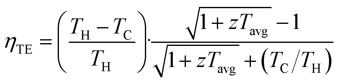 | (1) |
 | (2) |
From eqn (2), an efficient thermoelectric material requires a high Seebeck coefficient (S) to maintain a high potential difference across an applied thermal gradient, a high electrical conductivity (σ) for an efficient flow of charges, and a low total thermal conductivity (κ) to minimize thermal shorting. The numerator S2·σ in the zT equation is also known as the thermoelectric power factor (PF), while the denominator can be further expressed as κ = κe + κL, considering the electronic (κe) and lattice (κL) contributions. However, improving zT is not as straightforward as the equation depicts, because the three main performance parameters (S, σ, and κ) are adversely correlated, thus placing constraints on the maximum achievable zT.
While the power conversion efficiencies of the best performing lab-scale TE devices (12–13% at ΔT ≈ 500 K) and state-of-practice TE devices (6–8% at ΔT ≈ 700 K),12–19 are still far behind those of conventional heat engines (30–50%),20 the solid-state nature of TE devices and their direct heat-to-electricity conversion enables them to operate without moving parts and with minimal maintenance. Such durability enables TE devices to serve as the main power generation technology in deep space probes, in the form of radioisotope thermoelectric generators (RTGs), capable of harvesting heat released by the radioactively decaying nuclear fuel to power the Pioneer I and II, Voyager I and 11, Ulysses, Galileo, and Cassini space probes for >1 billion cumulative mission-hours without fail.21 In addition, the smallest working unit of a TE device is much smaller than that of conventional heat-to-electricity conversion technologies, enabling standalone functioning units to fit into the tight spaces in the fusion reactor with minimal disturbances to the existing functions. Therefore, Yamaguchi et al. proposed a technique called ‘topping’, where high temperature (∼1273 K) TE materials can be placed at the plasma-facing surfaces to harvest the temperature gradient that is unutilised by the heat cycle of the existing molten salt coolant, allowing TE devices to run in parallel, generating additional power without affecting the efficiency of the existing molten salt's heat cycle.22
The various classes of TE materials and their performances maximise at different temperatures, as shown in Fig. 2. Although many of the TE materials can achieve high zTs of >2, such as GeTe,23–34 PbTe,35–39 and SnSe,40–44 and others exhibit peak performances in the medium temperature range (473–973 K),45–53 such TE materials will not be considered for discussion in this review, as they overlap with the operating temperature range of the much more efficient existing heat cycle of the molten salt coolant. Instead, for reliable performance on the plasma-facing surfaces, one should select from the tried and tested high temperature (873–1273 K) TE materials that have been used or assessed for RTGs in deep space probes, such as Si1−xGex, La3−xTe4 and Yb14MgSb11 zintls.54 Promising materials such as B4C, oxides, and half Heuslers with high thermal stabilities should also be considered for heat harvesting from plasma-facing surfaces in fusion reactors. The properties of selected examples from these classes of high temperature TE materials are summarized in Table 1 and the details of each material class will be elaborated upon in the following sub-sections.
 | ||
| Fig. 2 Temperature-dependent figures-of-merit (zT) of state-of-the-art TE materials based on (Bi, Sb)2(Te, Se)3,55,56 Mg3(Sb, Bi)2,57 MgAgSb,58 GeTe,59 PbTe,38,60 SnSe,41,42 half Heusler alloys,61,62 B4C,63 Si0.8Ge0.2,64,65 Yb14MgSb11,66 La3−xTe4,67 and Pr3−xTe4.68 | ||
| Material | Type | zT peak | T peak zT (K) | κ peak zT (W m−1 K−1) | T M (K) | Ref. |
|---|---|---|---|---|---|---|
| Si0.94P0.06 | n | 0.60 | 1125 | 10 | 1687 | 69 |
| Si1−xGex (for RTGs) | n | 0.89 | 1073 | 3.80 | 1633 | 70 |
| Si0.8Ge0.2 + 10% P, nano | n | 1.84 | 1073 | 0.93 | 1633 | 65 |
| Si0.8Ge0.2 + 6 wt% Y2O3 | p | 1.81 | 1100 | 2.38 | 1633 | 64 |
| Si0.8Ge0.2 + 0.23 vol% SiC | n | 1.70 | 1173 | 1.90 | 1633 | 71 |
| Modulation doped (Si80Ge20)0.8(Si100P3)0.2 | n | 1.18 | 1173 | 4.00 | 1633 | 72 |
| Uniformly doped Si84Ge16P0.6 | n | 1.00 | 1173 | 3.86 | 1633 | 72 |
| Modulation doped (Si80Ge20)0.7(Si100B5)0.3 | p | 0.92 | 1173 | 3.75 | 1633 | 72 |
| Uniformly doped Si86Ge14P1.5 | p | 0.79 | 1173 | 2.87 | 1633 | 72 |
| La2.77Te4 | n | 1.13 | 1273 | 0.52 | 1992 | 73 |
| La1.9Ca1.1Te4 | n | 1.20 | 1275 | 0.90 | 1992 | 67 |
| Pr2.74Te4 | n | 1.70 | 1200 | 0.88 | 1773 | 68 |
| Yb14MnSb11 | p | 1.00 | 1273 | 0.70 | 1473 | 74 |
| Yb14Mg0.9Al0.1Sb11 | p | 1.25 | 1250 | 0.73 | 1473 | 66 |
| B6.5C | p | 1.06 | 1250 | 3.75 | 2620 | 63 |
| B9C + 0.5 at% Mg | p | 0.65 | 1300 | 5.00 | 2620 | 75 |
| B4C + 10 wt% HfB2 | p | 0.20 | 1000 | 4.28 | 2620 | 76 |
| SrB6 | n | 0.30 | 1073 | 10 | 2235 | 77 |
| CaB6 | n | 0.11 | 1073 | 10 | 2230 | 77 |
| (Nb0.64Ta0.36)0.8Ti0.2FeSb | p | 1.60 | 1200 | 3.37 | 61 | |
| Zr0.2Hf0.8NiSn0.985Sb0.015 | n | 1.09 | 1123 | 5.55 | 62 |
2.2. Silicon–germanium alloys (Si1−xGex)
From past research on high temperature materials for RTGs for deep space probes, Si1−xGex stands out due to its high thermal stability and melting points, where the liquidus points of Si and Si0.8Ge0.2 occur at 1687 and ∼1633 K, respectively.78 Since the 1970s, prototype Si1−xGex modules have been measured with hot and cold side temperatures of 1308 and 573 K respectively, in order to predict their performance when used in a RTG.79,80 Si1−xGex-based RTGs are known to operate at thermal gradients of 575–1275 K with a power conversion efficiency of ∼8%.12Despite the high cost of Ge, Si1−xGex materials are rather attractive choices due to the easy p- and n-type dopability,21,81 high abundance and low cost of Si, excellent tensile strength (>7000 psi), shock and vibration resistance.82 With x increasing from 0 to 0.2, the thermal conductivity of Si can be sharply reduced from ∼140 to <10 W m−1 K−1, due to the enhanced mass disorder and anharmonicity from the alloy scattering of the Ge dopants. From x = 0.2 to 0.8 however, the thermal conductivity reduction remains rather constant.83 Therefore, the most commonly reported compositions of Si1−xGex, as well as the best performing Si1−xGex-based materials have x = 0.2, although reasonably high performance can also be achieved with minimal Ge content of 1 atom% and using Si upcycled from waste solar panels.84
Incorporation of grain sizes of <100 nm has been used to achieve reductions in the lattice thermal conductivity to carrier mobility ratios of Si1−xGex, by exploiting the much larger phonon mean free path of Si1−xGex (up to 300 nm) as compared to that of electrons (5 nm).70,85 Even without Ge, fine-grained (∼0.8 μm) Si1−xPx pellets were also able to achieve a three-fold enhancement in peak zT as compared to the single-crystalline counterpart.69 The current record zT for n-type Si1−xGex is 1.84 at 1073 K, which was achieved by scattering a wide spectrum of phonons using dislocations, nanoscale amorphous and crystalline features (∼20 nm), and lowering the thermal conductivity to ∼0.93 W m−1 K−1. These defects were introduced during the synthesis which involved ball milling for 72 h and hot-pressing at 1323 K for 1 h with very fast heating and cooling rates.65
In a fusion reactor environment, where sudden transient surges in temperature may occur during plasma instabilities, there is a risk that the nano-sized grains may recrystallize into large grains, which will undo the features that contribute to its high performance. Therefore, it may be necessary to incorporate insoluble nano-scale secondary phase additives into the Si1−xGex matrix instead. The current record zT for p-type Si1−xGex is 1.81 at 1100 K, which was achieved by adding Y2O3 (60 nm) nano-powders in p-type Si0.8Ge0.2 to form in situ YSi2 nano-inclusions. Due to their matching crystal structures, these YSi2 nano-inclusions form coherent interfaces with the Si0.8Ge0.2 matrix, enhancing the Seebeck coefficient by the carrier filtering effect, while lowering the thermal conductivity by scattering phonons at the strained interface.64 A similar strategy was also successful in n-type Si0.8Ge0.2 after adding SiC nanoparticles (20–60 nm), leading to a high zT of 1.7 at 1173 K.71 As these additive materials have melting points >2000 K, they should remain stable even in the event of sudden temperature surges beyond 1273 K and continue to provide enhancements to the TE properties of Si1−xGex.
2.3. Lanthanum telluride (La3−xTe4) and Yb14(Mg,Mn)Sb11 zintl compounds
From a report on next-generation RTGs by NASA in 2017,54 n-type La3−xTe4 and p-type Yb14(Mg,Mn)Sb11 zintl compounds have been identified as potential candidate high temperature (873–1273 K) TE materials for RTGs, as they have high performances at ∼1273 K and high melting points of 1992 and 1473 K, respectively.73,86 In a study comparing the fundamental material parameters of various rare earth chalcogenides, such as the density of states carrier effective mass ( ) and the carrier mobility (μ), La3−xTe4 was highlighted as the compound with the highest
 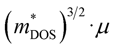 value, with a much higher μ of 11.5 cm2 V−1 s−1 and one of the lowest
 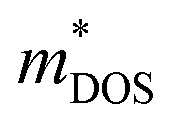 of 1.8 me, making it the most promising rare earth chalcogenide in terms of intrinsic electrical transport properties.87 Nevertheless, a
  of 1.8 me is still considered very high among other classes of TE materials, which is mainly contributed by the La 5d states resulting in a large peak in the density of states near the Fermi level, which results in high Seebeck coefficients. Carrier concentration adjustment through stoichiometric control can usually be used to optimize the zT of La3−xTe4 materials. Starting from the insulating composition of La2Te3 (or La2.67Te4), as more La is added, each La atom will ionize to form La3+ ions and donate 3 electrons, such that La3Te4 will essentially have metallic conduction. Therefore, x in La3−xTe4 is usually tuned between 0 and 0.33, where the best zT of 1.13 at 1273 K was achieved by the x = 0.23 sample, among La3−xTe4 samples synthesized by mechanical alloying.73 A finer control of the carrier concentration can be achieved by doping Ca on the La sites, where an improved peak zT of 1.2 at 1275 K was achieved by La1.9Ca1.1Te4.67 To address the high reactivity of La especially at high temperatures, adding 10 vol% of Ni during the mechanical alloying synthesis of La2.74Te4 can improve its oxidation resistance, by forming dense protective La2NiO4/Ni2Te3O8/NiO oxide interface layers.88 However, it was discovered in 2018 that the Pr2.74Te4 material was able to achieve a much higher zT of 1.70 at 1200 K, which is a ∼50% improvement over the La3−xTe4 materials.68 Contrary to the La3+ ions present in La3−xTe4, the Pr3+ ions have three 4f valence electrons, where the density-of-states contribution of the f orbitals dominates near the Fermi level in the range of interest for Seebeck coefficient enhancement. However, unlike La3−xTe4, the temperature-dependent zT data reveal the onset of a decreasing trend near the maximum temperature of 1250 K for the Pr2.74Te4 material.
The p-type Yb14(Mg,Mn)Sb11 zintl compounds have attracted the attention of the TE research community due to their complex crystal structures consisting of Yb2+ cations, isolated (Mg,Mn)Sb4 tetrahedra, linear [Sb3]7− units, and isolated Sb3− anions, leading to their low lattice thermal conductivities, with most of their phonon dispersion containing low velocity optical phonon modes.74,89,90 In a more recent study, it was revealed that a second high valley degenerate (Nv = 8) band that can be utilised for hole transport at higher temperatures or at higher doping levels, is responsible for the large density-of-states effective masses of ∼3 me, as well as the high performance of Yb14(Mg,Mn)Sb11.66 In addition, there is a large variety of similar compounds where the Yb and Mn sites are replaced with a variety of other elements, such as Ca, Mg, Al, and Zn, providing plenty of potential for developing various solid solutions for further optimization.74 For example, while pristine Yb14MnSb11 was reported to have a zT of ∼1 at 1273 K,74 the Yb14Mg0.9Al0.1Sb11 solid solution has an improved zT of 1.25 at 1250 K.66 However, similar to the case of Pr2.74Te4, the temperature-dependent zT data of the Yb14(Mg,Mn)Sb11 zintl compounds also reveal the onset of a decreasing trend near 1273 K. Among the Yb14MSb11 (M = Mg, Mn, Zn) phases, Yb14ZnSb11 demonstrated the best resistance to oxidation, a finding that can lead to further passivation optimization.86
2.4. Boron carbide (B4C) and other borides
While B4C has never been used in RTGs before, it has been suggested before in the 1990s as a potential TE material on the first wall and divertor surfaces,91 due to its excellent thermal stability (melting point of 2623 K). Despite the commonly known simple composition that is akin to a tetraboride, B4C is considered as a higher boride with a complex crystal structure with B12 and B11C icosahedra linked by C–B–C, C–B–B, or C–vacancy–C chains, where the exact structure varies with the precise chemical composition.92–94B4C is a persistently p-type material due to the overall deficiency in valence electrons. Stoichiometric B4C is a material with a high Seebeck coefficient of ∼100 μV K−1 and low electrical conductivity of ∼1 S cm−1 at room temperature.63 Unlike most highly doped semiconductors, B4C demonstrates a variable range hopping carrier transport behaviour, where both the Seebeck coefficient and electrical conductivity increase with increasing temperatures to ∼250 μV K−1 and ∼50 S cm−1 at 1250 K, making it especially suited for very high temperature applications.76 Having excess B in B4C materials induces a deficiency of C, which weakens the atomic chains between the icosahedra,75,95 simultaneously lowering the thermal conductivity and improving the electrical conductivity, up to an optimum composition of B6.5C. A peak zT of 1.06 was achieved by the B6.5C material at 1250 K, which is drastically higher than that of B4C (zT ∼0.02).63 Based on this behaviour, it is not feasible to favour n-type conduction by adding an excess amount of the more electron-rich C. To date, there has not been an n-type B4C-based material with comparable performances reported yet, and published studies on B4C-based TE device modules are rare. Using a laser-based joining technology with a fast heating rate, Börner et al. fabricated a 14-leg TE device module using B7C and TiOx (x < 2) as the p- and n-type legs respectively. TiOx was chosen as the n-type counterpart to be paired with B7C due to its reasonable zT of 0.2, high thermal stability and comparable coefficient of thermal expansion. Ti-containing Ag–Cu was used as the brazing foil to bond the TE legs to the copper interconnect electrodes and also to bond the copper electrodes to the AlN substrates. While the power conversion efficiency or heat flux was not reported, the TE device had a maximum power output of 75 mW and voltage of 0.25 V when a thermal gradient of 312 K was applied.96
While there are many other boride compounds which all have very high melting points, B6.5C still stands out as the best performing boride material at temperatures above 1000 K.93 With the exception of the divalent hexaborides and the homologous series of rare earth (RE) borocarbonitride compounds such as REB15.5CN and REB22C2N, most borides are intrinsically p-type. One of the best performing rare earth borocarbonitrides is 1.5 at% VB2-seeded YB22C2N, with a Seebeck coefficient of −20–−80 μV K−1 and a low thermal conductivity of ∼0.9 W m−1 K−1, but it possesses a low zT of <0.001 even at a high temperature of 1050 K.97 For metal hexaborides, intermediate-valent hexaborides such as CeB6 and SmB6 had small metallic-like positive Seebeck coefficients of several μV K−1, while divalent hexaborides from YbB6, to SrB6, to CaB6, and possessed large negative Seebeck coefficients of −100 to −273 μV K−1 at 1073 K.77 These compounds are more promising as n-type boride-based counterparts to B4C, where SrB6 and CaB6 were measured to have peak zTs of ∼0.3 and ∼0.1 respectively at 1073 K. The lack of saturation in the temperature-dependent zT trend of SrB6 with increasing temperature implies the potential for a higher zT at higher temperatures of 1273 K.
2.5. Half Heusler alloys
Half Heusler alloys are highly promising TE materials due to their very high PFs with p-type Nb0.95Ti0.05FeSb being able to achieve a record-breaking room-temperature PF of ∼10![[thin space (1/6-em)]](https://www.rsc.org/images/entities/char_2009.gif) 600 μW m−1 K−2.98 The origin of such high PFs was revealed to be due to the crystal symmetry-protected non-bonding orbitals at the band edge, which have suppressed carrier-acoustic phonon interactions and low deformation potentials.99 In addition, half Heusler alloys possess excellent thermal stabilities and mechanical properties and they usually form more robust junctions with metal electrodes, as compared to other TE semiconductors.100,101 Half Heusler compounds with general formulae of XYZ consist of three interpenetrating face-centred cubic sub-lattices, where the X atomic position is occupied by transition metal elements with low electronegativities (e.g. Groups 3–5) and sometimes f-block elements, Y atomic position is occupied by transition metals with higher electronegativities (e.g. Groups 8–10), and Z atomic position is occupied by p-block elements (e.g. Groups 13–15).102,103
600 μW m−1 K−2.98 The origin of such high PFs was revealed to be due to the crystal symmetry-protected non-bonding orbitals at the band edge, which have suppressed carrier-acoustic phonon interactions and low deformation potentials.99 In addition, half Heusler alloys possess excellent thermal stabilities and mechanical properties and they usually form more robust junctions with metal electrodes, as compared to other TE semiconductors.100,101 Half Heusler compounds with general formulae of XYZ consist of three interpenetrating face-centred cubic sub-lattices, where the X atomic position is occupied by transition metal elements with low electronegativities (e.g. Groups 3–5) and sometimes f-block elements, Y atomic position is occupied by transition metals with higher electronegativities (e.g. Groups 8–10), and Z atomic position is occupied by p-block elements (e.g. Groups 13–15).102,103
For p-type half Heusler alloys, the highest zT of 1.6 at 1200 K was achieved by (Nb0.64Ta0.36)0.8Ti0.2FeSb. The isoelectronic substitution of Ta at the Nb site was effective in scattering phonons while maintaining good electrical properties. The very high melting point and density of Ta, as compared to the other elements in the alloy, present additional challenges when attempting to synthesize single-phase solid solutions, which can only be overcome by using levitation melting.61 For n-type half Heusler alloys, the highest zT of 1.09 at 1123 K was realised by Zr0.2Hf0.8NiSn0.985Sb0.015, where the introduced local atomic disorder that contributes to thermal conductivity reduction has a negligible effect on the electron scattering process and the conduction band structure, allowing the alloy to maintain its high electron mobility.62
Due to its high zTs and high-temperature mechanical and thermal stabilities, Zhang et al. previously explored the feasibility of nanostructured n-type Hf0.25Zr0.75NiSn0.99Sb0.01 for nuclear applications due to its high-density of grain boundaries, which are expected to lead to improved irradiation damage resistance. The samples were irradiated with 2.5 MeV protons to a fluence of 2 × 1016 cm−2 under masks to create irradiated and non-irradiated regions within the same sample, so as to simultaneously characterize both regions by scanning thermal microscopy. While no statistically significant difference in the Seebeck coefficients between the two regions was observed from room temperature to 473 K, the irradiated regions were found to have ∼30% and ∼14% lower electrical and thermal conductivities respectively, as compared to the non-irradiated regions at room temperature.104
3. Practical considerations of plasma-facing TE devices in fusion reactors
3.1. Effects of plasma ions
Plasma-facing TE devices will experience bombardment of energetic ions (e.g. He ions), which will collide with the device module surface and eject atoms from the surface material, as shown in Fig. 3a. Smaller low Z atoms (especially from Si1−xGex and B4C) will be more easily knocked out of their positions by the incoming energetic ions from the plasma, as compared to larger high Z atoms. In addition, implantation of He gas or hydrogen isotopes can also occur as the energetic ions from the plasma striking a target can get lodged within its lattice to form interstitial defects, which will eventually saturate and coalesce into gas bubbles. To limit the damage to the TE material and device components, a layer of W armour material will need to be placed between the TE device and the plasma, where it can protect the TE device from erosion due to its high Z and direct gas implantation. For example, when W at 973 K is exposed to 3 keV He+ irradiation at a fluence of 3 × 10²⁰ He+ ions per m2, the He+ ions penetrate a few nm deep in the W layer, while the resulting He bubbles (∼10 nm diameter) can diffuse >30 nm deep into the W layer.105 At higher temperatures, the mobility of the He interstitial–vacancy complexes increases, enabling larger He gas bubbles to form with greater diffusion depths. Conversely, under a pure D plasma, D retention in W has been found to decrease with increasing temperatures above 700 K due to the depopulation of lower energy trap sites, while the D retention in W decreases by one or two orders of magnitude when using a D/He mixture plasma due to the nano-scale He bubble layer acting as a barrier against D diffusion.106 In any case, a W layer of sufficient thickness should be able to effectively protect the TE device against plasma-induced gas implantation but not against He or hydrogen isotope formation within the TE materials and device components due to transmutation by neutron irradiation, which will be elaborated in detail in the next sub-section.107,108 However, the disadvantage of high Z armour materials over their low Z counterparts is that if any of the armour materials fall into the plasma, high Z materials are more effective at quenching the plasma and stopping the fusion reaction.8 When using a high Z armour material such as W, the adhesion between the armour material and the reactor wall becomes even more crucial.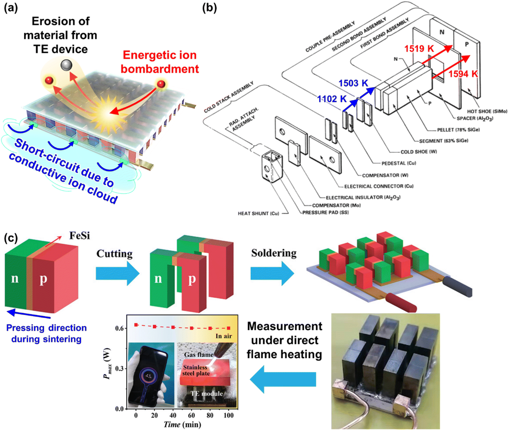 | ||
| Fig. 3 (a) Effects of fusion reactor plasma on TE device modules. (b) Expanded view of standard components in a Si1−xGex-based material unicouple for radioisotope thermoelectric generators and their recommended bonding temperatures. Copyright 1995, AIP Publishing LLC. Used with permission from ref. 80, AIP Publishing LLC. (c) Fabrication process schematic of the electrode-free FeSi2-based TE device module and performance testing under direct flame heating in open air. Copyright 2022, Wiley. Used with permission from ref. 112, John Wiley & Sons, Ltd. | ||
Coincidentally, W and Mo have been reported to be good electrode materials for Si1−xGex-based TE device modules in radioisotope thermoelectric generators, due to their similar coefficients of thermal expansion (CTEs) of 4–5 × 10⁻⁶ K−1,109 making these Si1−xGex-based TE device modules potentially adaptable to a fusion reactor environment. An example of an assembly of standard components in a Si1−xGex-based material unicouple for radioisotope thermoelectric generators is shown in Fig. 3b,80 where these unicouples will all be connected electrically in series in a TE device module to build up a sufficient voltage, leaving gaps between the TE material legs to prevent short-circuiting. However, since a plasma is an electrically conductive ion cloud, any ionized gases that happen to be in these gaps may cause a short-circuit, as shown in Fig. 3a, leading to a drop in the device output voltage. Therefore, it is also necessary to fill these gaps with an electrically insulating material to act as a physical barrier against electrical short circuit by ionised gases. A potential candidate for such electrically insulating materials would be SiC or SiC fibre composites as they have also been a well-known promising candidate for plasma-facing armour materials besides W.110,111
3.2. Thermal effects from the plasma
First, in a high temperature and low-pressure environment, sublimation from TE material surfaces will be a bigger issue not only because of degradation of TE performance and service stability, but also because of contamination of the plasma. While materials such as La3−xTe4 and Yb14MgSb11 have higher melting points than Si1−xGex, the sublimation rates of La3−xTe4 and Yb14MgSb11 at 1273 K are 8 × 10⁻³ and 1 × 10⁻³ g cm−2 h−1 respectively, which are two orders of magnitude higher than that of Si1−xGex (4.8 × 10⁻⁵ g cm−2 h−1).109 In addition, telluride-based radioisotope thermoelectric generators need to be sealed with 1 atm of an inert Ar–He cover gas in order to minimize sublimation at high temperatures in the vacuum of space.12 These sublimations can be minimised by depositing a coating of Si3N4 or SiO2.21,80,109,113 Therefore, Si1−xGex and B4C seem to be more viable choices as they have high thermal stabilities and are made from relatively more abundant elements.The pulsed operation of the plasma will expose the materials to sudden temperature increases and drops with typical pulse lengths of a few minutes for ITER. In addition, instabilities in the plasma may result in the formation of plasma Edge-Localised Modes (ELMs), which are analogous to solar flares from the Sun. Such transient thermal loads from the ELMs can have pulse durations in the millisecond range. Due to the short pulse durations of ELMs, the damage region will usually be limited to a few hundred microns. An armour layer a few millimetres thick may protect the underlying TE material against thermal shock from the ELMs, but the thermal shocks from longer pulse durations from normal plasma pulsed operation may still be experienced by the TE material. When the material is first heated quickly on one side, thermal shock can occur as the thermal expansion on the hot side is constrained by the surrounding colder regions, generating compressive stresses beyond the yield strength of the material. As these materials undergo plastic deformation, they will be unable to return to their original state during thermal contraction when cooled down, converting the compressive stresses into tensile stresses. After many heat–cool cycles, cracks in the material can accumulate until mechanical fracture occurs.8
Thermal shock resistance (R′) can be expressed as a function of fracture strength (σf), thermal conductivity (κ), Poisson's ratio (ν), Young's modulus (E), and the coefficient of thermal expansion (α), by using the equation R′ = σf·κ(1 – ν)/(E·α).114 To improve resistance to cracking due to thermal shock, the orientation of the grain boundaries can be used to guide the crack propagation, where the crack penetration depth is the shortest for W samples with layered grains stacked along the direction of the thermal gradient (longitudinal grain orientation), followed by samples with columnar grains (transverse grain orientation), and the deepest cracks were observed in the recrystallized samples.8 Fibrous additives have also been added to reinforce various ceramics to improve their fracture toughness through toughening mechanisms such as CNT pull-out, the bridging effect and crack deflection.115–117 Maki et al. demonstrated that the carbon nanotubes (CNTs) in B4C composites can be aligned with their lengths perpendicular to the hot-pressing direction, where the resulting composite pellets have slightly anisotropic thermomechanical properties.114 In general, with increasing CNT content, the composites with mechanical properties measured perpendicular to the hot-pressing direction have more significant decreases in Young's modulus, Vickers hardness, and coefficient of thermal expansion, and more significant increases in the fracture toughness and thermal conductivities. The sample with the highest thermal shock resistance was found to be the sample with the 10 vol% CNTs, perpendicular to the pressing direction.114 Besides improving the thermomechanical properties of B4C, adding CNTs can also improve the electrical conductivity of the resulting B4C composites, which may improve the zT.
Besides the thermal stability of the active TE materials themselves, another major cause of performance degradation under prolonged operation in TEGs is usually the degradation of contact quality between the active TE material and the interconnecting electrode materials. High temperature TE materials are usually ceramic in nature, while the interconnecting electrode materials are usually metals. However, most ceramics usually have poor wetting with most metals.96,118 Therefore, the interface material layers (e.g. metallization layer) between the active TE material and the interconnecting electrodes need to be carefully chosen based on their ability to have sufficient interdiffusion with the TE material to maintain a strong adhesion, but not too much such that the diffusion layer grows uncontrollably under prolonged operation. The phases formed at the diffusion layer between the materials must also have high electrical and thermal conductivities in order to minimize the contact resistances. However, given the strict material requirements for fusion plasma-facing materials, the material selection for suitable interface materials may be severely limited, while the stacking of too many different materials may lead to more complications under the extreme operating conditions that will be difficult to troubleshoot. To eliminate such problems, electrode-free device fabrication strategies that involve the direct bonding of p- and n-type material legs can be considered. Joining of similar ceramic materials would eliminate the problems associated with metal-ceramic contacts, such as poor wetting and stresses due to thermal expansion coefficient mismatch. Qiu et al. fabricated a FeSi2-based device by stacking the loading of the p-type Al-doped and n-type Ir-doped FeSi2 powders in the graphite die, with a FeSi metallization layer in between them, followed by spark plasma sintering.112 From the resulting stacked pellet, the p- and n-type layers can be electrically separated by cutting out a gap in between them, leaving the strongly sintered connection for the hot side, which can withstand heating by a flame, as demonstrated in Fig. 3c.
3.3. Neutron irradiation effects: transmutation
Although TE materials have been used to harvest heat from nuclear sources in radioisotope thermoelectric generators (RTGs), the radioisotope fuel (usually 238PuO2) is usually chosen based on its half-life, power density and lack of highly penetrating radiation (e.g. gamma rays and neutrons), so that minimal radiation shielding is required. In addition, without the need to use the emitted neutrons for other processes, the TE materials in RTGs can be allowed to operate behind a radiation shield, with little concern for radiation damage. Therefore, the TE materials in RTGs are not specially designed to withstand the high levels of neutron irradiation experienced by plasma-facing surfaces in a fusion reactor (neutron flux at 14.1 MeV = 1.5–5.0 × 1014 cm−2 s−1).11 Therefore, special material considerations have to be taken into account considering the extremely high neutron irradiation damage of 150–200 dpa (displacements per atom) from a fusion reactor.10,119One of the well-known major appeals of fusion energy over fission energy is that it does not create long-lived radioactive nuclear waste which requires prolonged storage. However, this will only be true if the usage of high-activating elements is minimized. High-activating elements (represented by the orange, blue, red and black elements in Fig. 4) refer to those that will transmute to form long-lived radionuclides after being subjected to neutron irradiation. Therefore, low-activating elements (represented by the green, yellow, and pink elements in Fig. 4), which can be recycled or disposed in non-active landfills ∼100 years after removal from the reactor, are generally preferred for usage in regions of the fusion reactor that experience a high fluence of neutrons.120,121 In addition, the usage of low-activating materials provides a passive safety advantage by generating less heat by radioactive decay,122 making their thermal stabilities and performances more predictable.
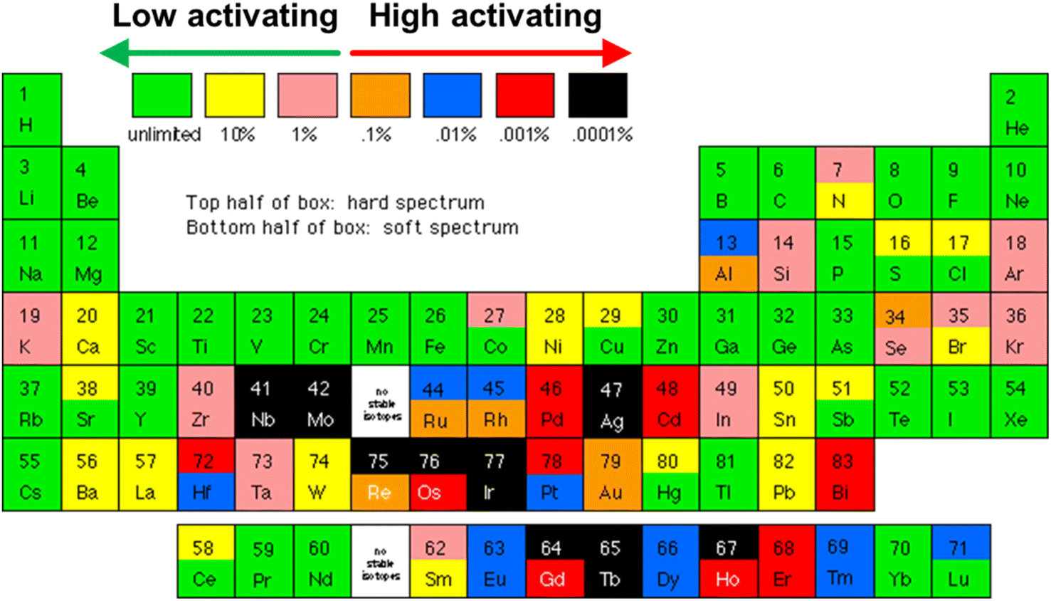 | ||
| Fig. 4 Periodic table of low and high activation elements, assuming a 5 MW m−2 flux for 4 years. Image obtained from the open web [http://qedfusion.org/LIB/PROPS/SAFETY/class_c.shtml] on 29 Mar 2024. | ||
Among the high temperature TE materials considered previously, Si1−xGex and B4C are the most sustainable as their matrix phases are mostly made with rather earth abundant and low-activating elements. This means that besides the high availability of raw materials, they will also have a reduced burden on the waste disposal process when decommissioning the fusion reactor as they do not need to be stored for a very long time in order to radioactively decay into low-level waste. In contrast, the scarcity of elements such as Te and Yb and the high-activating nature of Yb will make La3−xTe4 and Yb14MgSb11 less sustainable choices.
B has been known to have a relative atomic mass of 10.811 amu as it is an average of ∼20% of 10B and ∼80% of 11B isotopes. While the 11B isotope does not transmute easily, the 10B isotope has a high thermal neutron absorption cross-section,123 readily absorbing neutrons to form 7Li and α-particles (He2+ ions).124,125 Significant amounts of He will hence be produced by the 10B atoms, which effectively comprises ∼16% of all atoms in B4C. It is also for this reason that B4C has been used as a burnable neutron absorber in the control rods of nuclear fission reactors, where its neutron absorption ability will degrade over time.126 For long lasting neutron absorption, isotopes 176Hf to 179Hf all remain chemically unchanged when absorbing neutrons, while 180Hf absorbs a neutron to form 181Hf which beta-decays to form 181Ta.127 Therefore, to avoid excessive degradation of TE properties under neutron irradiation, usage of B4C as TE materials may require neutron shielding on the plasma-facing side with a layer of Hf, which is unfortunately a high-activating element. Such a TE device would be a highly effective neutron shield, which can be useful when placed in front of windows for neutron-sensitive diagnostics in the fusion reactor. However, if placed on the first wall, the Hf–B4C material would also block neutrons from reaching the blanket, reducing the Tritium breeding efficiency. Such placement would forbid the use of a Hf layer and require the B4C material to be isotopically enriched with the non-absorbing 11B isotope. In the 1990s, B4C with 90% 10B isotope enrichment was very expensive and cost USD 4000–5000 kg−1, as compared to B4C with natural abundance (USD 15–75 kg−1).126 The price and availability of the enriched 11B4C made from the 11B waste product of the enrichment process would therefore depend heavily on the current demand for 90% enriched 10B4C.
With a magnetic-confinement fusion energy (MFE) neutron spectrum, 3862 atomic ppm of transmutation products can be produced from SiC, where Mg, Al and P account for 60, 20 and 0.4% of all transmutation products, respectively.128 Since the majority of these transmutation products all have proton numbers higher than that of C, they can be expected to originate from the transmutation of Si. While Al is known to be a deep-level acceptor defect in Si, P is an n-type dopant while Mg can react with Si to form Mg2Si,111 which is a known n-type TE material. While such transmutation reactions will not be expected to greatly impact the performance of n-type Si1−xGex TE materials, having electron-donating impurities will be deleterious to p-type Si1−xGex TE materials. Therefore, it may be useful to employ a functionally graded B doping design, where the plasma-facing hot end can be much more heavily doped with B, not just for the additional holes to balance the effects of the electron-donating impurities, but also to make use of the high neutron absorption cross-section of B to reduce the extent of transmutation in the rest of the Si1−xGex material.
3.4. Neutron irradiation effects: void swelling and He bubbles
In addition to the chemical transformation of elements by transmutation, the immediate kinetic effects of neutron bombardment are atomic displacement cascades, which will eventually develop into microstructures that will affect the mechanical strength and dimensional stability of the material.129 Although high temperature TE materials are usually non-load bearing ceramics with less stringent mechanical strength requirements as compared to the more well-studied structural alloys like Reduced Activation Ferritic Martensitic (RAFM) steels or the Nanostructured Ferritic Alloys (NFA), mechanical strength is still highly desired in order to withstand the high thermal stresses and to prevent delamination of the TE device parts from the reactor wall surface.First, the energetic neutron collides with an atom which will gain the kinetic energy to be a Primary Knock-on Atom (PKA). The PKA then collides with another atom and knock it out of its original position to form a Frenkel pair, which consists of a vacancy and a self-interstitial atom (SIA), as shown in Fig. 5a. From here, a displacement cascade is initiated, which can trigger the formation of different microstructural defects, depending on certain transition temperatures that can be approximately scaled to the melting point of the material (TM). While it is possible for the vacancies and SIAs to recombine and restore the original atomic position in the lattice site, it may not happen easily due to SIAs having much higher mobilities than vacancies, especially at lower temperatures (T < 0.2 TM). SIAs combine with each other to form clustered geometries such as stacking fault tetrahedra (SFT) and interstitial dislocation loops or Frank loops.
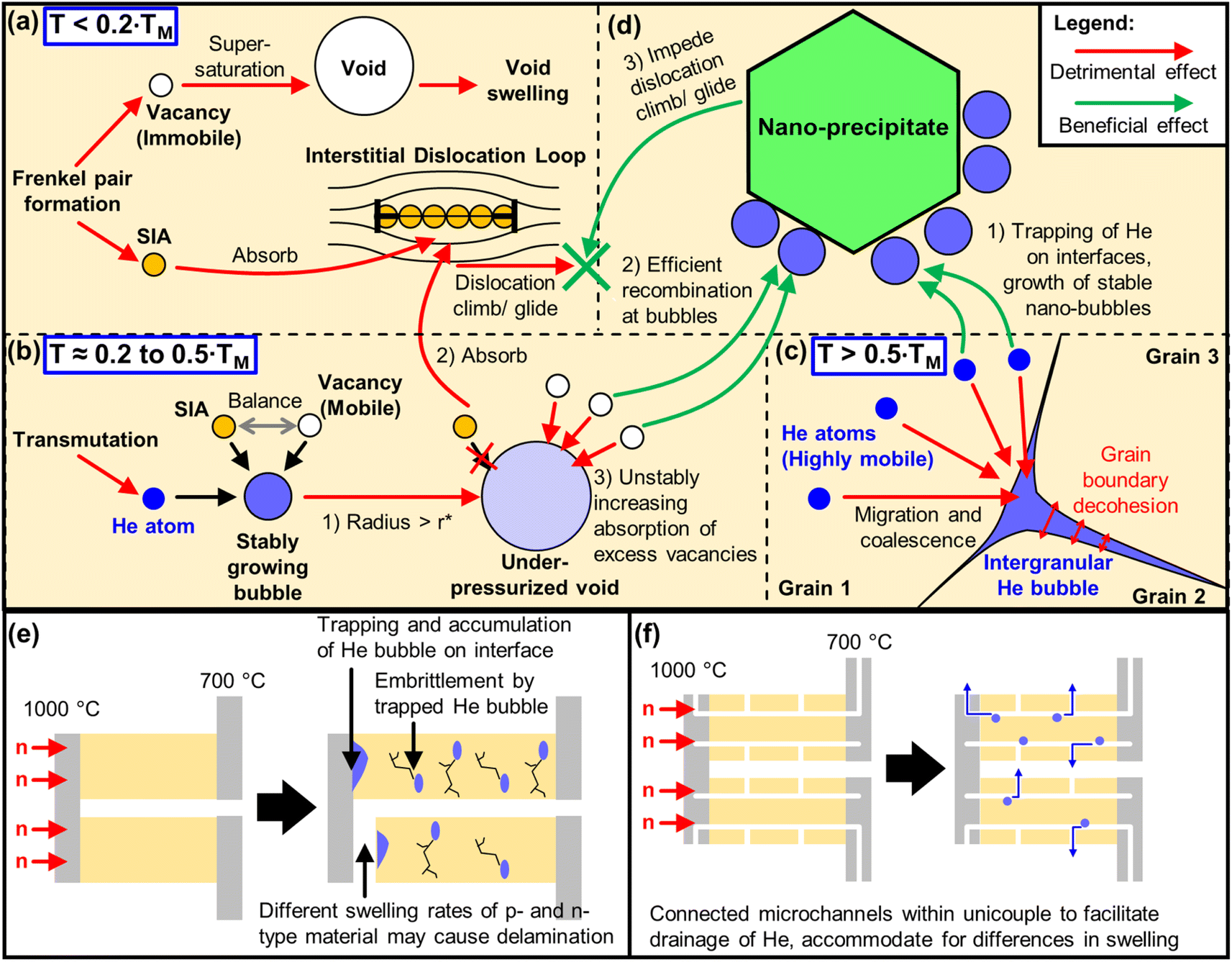 | ||
| Fig. 5 (a) Origin of void swelling at lower temperatures (T < 0.2 TM), where self-interstitial atoms (SIAs) are mobile while vacancies are immobile. (b) Origin of He-promoted void swelling from the combined effects of displacement damage and transmutation generated He atoms, at intermediate temperatures (T ≈ 0.2 to 0.5 TM) where both SIAs and vacancies are mobile. (c) Origin of He embrittlement at high temperatures (T > 0.5 TM) where He atoms are highly mobile. (d) Schematic of how an intragranular nanoprecipitate can alleviate void swelling and He embrittlement. Schematic of the potential macroscopic effects of a TE device unicouple under neutron irradiation and a temperature gradient of 973–1273 K, (e) without and (f) with connected open microchannels. | ||
In general, most microstructural defects can function as traps or sinks for these atomic defects. For example, in Si, impurity atoms such as B and P can trap both vacancies and Si interstitials, where in the Watkins replacement mechanism, Si interstitials can replace the substitutional dopant, converting it into an interstitial dopant.130 However, interstitial dislocation loops in most materials preferentially absorb interstitials over vacancies, especially during the dislocation climb, as shown in Fig. 5a. This leaves behind many vacancies with no interstitials to recombine with them. Once the vacancies reach supersaturation, they condense to form voids and eventually lead to macroscopic swelling and crack formation in the material, deteriorating the dimensional stability and mechanical properties. In the case of alumina (α-Al2O3, HCP structure), the more pronounced nucleation and growth of the interstitial dislocation loops on the (0001) basal plane in the hexagonal structure of alumina causes extensive biased absorption of interstitials. Whereas for spinel (MgAl2O4, FCC structure) single crystals, the more ‘disordered’ {111} dislocation loops of spinel do not grow beyond 100 nm in size, limiting its preferential absorption of SIA, allowing more beneficial recombination events to occur between its interstitials and vacancies, causing spinel to have a much better resistance to irradiation-induced swelling than alumina.131 The difference in the behaviour of the interstitial dislocation loops in the ferritic (BCC structure) and austenitic (FCC structure) steels has also been highlighted as one of the possible reasons why ferritic steels have better swelling resistance than austenitic steels.10 While the differences in the behaviour of interstitial dislocation loops can be explained by the crystal structures in these notable examples, there are still some exceptions to these observed trends that cannot be explained by any general crystal design guidelines for improved swelling resistance.
Besides the displacement cascade damage from the PKA, neutrons also trigger multistep transmutations in material atoms, many of which result in the generation of He within the material. The damage from He is usually more serious due to its insolubility in most solid materials, which if not managed properly, can promote swelling by underpressurized cavities at intermediate temperatures (T ≈ 0.2 to 0.5 TM), where both SIAs and vacancies are mobile. The onset of He-promoted void swelling is well described as a critical bubble with a radius (r*) and He content (c*). Bubbles with radii smaller than r* are stable as they maintain a balance between the absorption of vacancies and SIAs, and their growth only comes from the absorption of He atoms. However, as shown in Fig. 5b, once the bubble grows to a critical size of r* (step 1), adding a single He atom or vacancy will cause the bubble to grow into an underpressurized void by rapidly absorbing the vacancies, which are in excess after the preferential absorption of SIAs by the interstitial dislocation loops (steps 2 & 3). It should also be noted that in vacancy-rich regions, bubbles represent the configuration with the lowest free energy, implying that it is energetically favourable for the excess vacancies to be absorbed by bubbles.132 At even higher temperatures of T > 0.5 TM, where most residual small defect clusters in the matrix have already been recombined, the highly mobile He atoms migrate from the matrix to the grain boundaries where they will be trapped, coalesce into a He bubble and continue to grow by absorbing more He atoms,10 as shown in Fig. 5c. These large intergranular He bubbles can lead to decohesion between the grain boundaries, initiating very brittle intergranular fracture paths, resulting in He embrittlement.132
When placed under a thermal gradient of 973–1273 K, B4C will fall in an intermediate homologous temperature range of 0.37 to 0.49 TM, where it will be mainly subjected to He-promoted void swelling, whereas Si0.8Ge0.2 will fall in a high homologous temperature range of 0.60 to 0.78 TM, where it will be mainly subjected to He-embrittlement. To understand the material modifications required to improve void swelling resistance in B4C in the intermediate temperature range, one can refer to the successful strategies used in the structural steels. While a small amount of He can promote void swelling, having a high density of stable nano-scale He bubbles can in principle, sequester high levels of He and serve as effective sinks that mitigate all manifestations of displacement damage,132 reducing the net swelling as a result. Using austenitic stainless steel as an example, after 4 MeV Ni ion irradiation at 898 K at a damage level of 70 dpa, the alloy that was pre-treated by implantation with 1400 atomic ppm of He at room temperature and showed a very high density of ∼20 nm small He bubbles, was able to limit irradiation-induced swelling to 1%, as compared to the untreated sample which suffered from a large swelling of 18%.133,134
To increase the density of He nano-bubbles, the He generated by transmutation can be partitioned and distributed even more uniformly by incorporating nano-scale precipitates in the material, which trap He in small bubbles at the matrix–precipitate interface, such that these bubbles are all smaller than the critical bubble size and He content (see Fig. 5d, Step 1).132 A successful example would be the Fe-based MA957 alloy, with commercial compositions containing 14 wt% Cr, 0.9% Ti, 0.3% Mo, and 0.25% Y2O3,135 falling under a class of nanostructured ferritic alloys or nano-dispersion strengthened ferritic alloys (NFA). After irradiation with 9 dpa and 380 atomic ppm He at 773 K (∼0.42 TM), it was revealed that the high number density (8.0 × 10²³ m−3) of Y–Ti–O rich nanofeatures (∼3 nm) in the MA957 alloy was able to trap a high density (1.5 × 10²² m−3) of bubbles (4.3 nm). These He nano-bubbles are effective sinks capable of trapping more He and act as efficient recombination centres for vacancies and SIAs (see Fig. 5d, step 2).136 In addition, these nano-precipitates can also impede the dislocation climb and glide,132 which can be useful in hindering the selective absorption of interstitials by the climbing interstitial dislocation loops, thereby limiting the occurrence of vacancy supersaturation. Similar to the in situ precipitation of Y–Ti–O rich nanofeatures from the addition of Y2O3 in MA957 alloys, adding Y2O3 (60 nm) in p-type Si0.8Ge0.2 will form in situ YSi2 nano-inclusions, which increases the Seebeck coefficient while lowering the thermal conductivity. Overall, while this strategy was highly effective in enhancing the zT from 1 to 1.81 in p-type Si0.8Ge0.2,64 using smaller Y2O3 nanoparticles may potentially be highly effective in improving its irradiation damage resistance.
In the scenario of a fusion reactor, under prolonged irradiation at high neutron fluence, and coupled with the very high mobility of He atoms at high temperatures (relative to TM), the microstructural features in the material may not be able to trap the large quantities of He generated. Referring to an example of how excess He gets released from a ceramic material at relatively high temperatures, SiC pellets were first irradiated with 1018 He ions per cm2 at 1000 K. The crater-like inclusions (∼1 μm) observed on the surface have a conical shaped cross-section that goes >500 nm into the surface, which implies an accumulation of excess gas pressure in the bubbles that were nucleated ∼500 nm deep into the damage layer, swelling outward when closer to the surface, followed by an explosive rupture of the bubble to form a crater.137 Since the rupturing occurred in SiC at T = 0.42 TM, it is reasonable to assume that this behaviour may also be reflected in B4C at 1273 K (T = 0.49 TM) and would be even more pronounced in Si0.8Ge0.2 at T = 0.78 TM, enough to overwhelm and saturate all the He sinks within the material and escape the material.
When the TE material is bonded to electrodes and assembled into a device, besides the rupturing of the He bubbles, the presence of a thermal gradient may favour the bulk diffusion of He towards one side and depositing He onto the interface between the TE material and the electrode layer, which would be severely damaging to the electrical contacts, as shown in Fig. 5e. In addition, due to the differences in doping or defects present in the p-type and n-type legs, the sink strengths and swelling resistance under the same irradiation will also be different, potentially causing one side to swell more than the other side. In such cases, macroscopic design features may need to be incorporated into the material to ensure proper and safe drainage of He gas. As exposed surfaces are unsaturable sinks, a possible method to alleviate the uncontrolled accumulation and rupture of the He bubbles would be to introduce microchannels within the material that are continuously connected and open to the surrounding atmosphere, as shown in Fig. 5f. Such microchannels can also be designed to redirect bulk quantities of trapped He to escape the material through the exposed surfaces instead of pushing against the electrode interfaces. An example of a TE material designed with continuous open pores was achieved by Zhang et al., where Bi2Te3 materials were 3D printed with gyroid structures by direct ink writing of the extruded slurry followed by annealing in an inert atmosphere for densification.138–140 These structures with a high specific surface area are designed for potential applications in exhaust pipes, where they can allow hot gases to flow through while harvesting the waste heat along the thermal gradient of the gas flow.141 Contrary to the recommended material design features with high sink strength densities that partition and trap He into a high number density of nano-bubbles, it may instead be more favourable to promote the high mobility of He atoms within the material at high temperatures, allowing them to quickly diffuse to the exposed surfaces of the microchannels along a concentration gradient and escape the material. Such decisions would greatly depend on the total exposed surface area of the microchannels, rate of He generation within the material, the binding strength of He on the microstructural traps or the ability of He to desorb from those traps at the given temperature.
3.5. Impact of the material and device design on heat transfer
In general, as there is a rather strong overlap between the strategies used to improve neutron irradiation damage resistance and many of the defect engineering strategies for TE performance enhancement (often by reducing the thermal conductivity relative to the power factor),142 state-of-the-art high temperature TE materials do indeed have great potential to be used for direct heat-to-electricity conversion on plasma-facing surfaces in fusion reactors. However, in current fusion reactor designs, due to the high heat flux, the reactor walls must also have sufficiently high thermal conductivities to facilitate efficient heat dissipation from the armour layer to the coolant, to prevent the armour layer from overheating, recrystallizing, or melting. Whereas a material design that is purely focused on high thermal conductivity will go against the need for certain microstructural defects (e.g. substitutional point defects, nanoprecipitates, and grain boundaries) which are important sinks and traps to resist neutron irradiation damage.143 Therefore, with a compromise between the TE device efficiency, irradiation damage resistance, and the heat dissipation efficiency from the plasma-facing side in a fusion reactor, the TE device thermal resistance needs to be carefully tuned, as summarized in Fig. 6. | ||
| Fig. 6 Relationship map of factors to consider for TE device design in fusion reactors. | ||
Reducing the material's thermal conductivity (relative to its power factor), will improve zT and TE device efficiency but will affect the device thermal conductance, which will affect the heat removal from the armour surface, leading to the possibility of overheating and recrystallization of both the armour and TE materials. While a recrystallized material should theoretically have a higher thermal conductivity, any beneficial grain boundary orientation will be lost during recrystallization, causing it to be less resistant to thermal shock due to its lowered resistance to deep crack penetration.8 Besides, the other microstructures that were functioning as beneficial sinks may be annihilated after the recrystallization processes, possibly with the exception of insoluble secondary phase nanoprecipitates. With its reduced resistance to irradiation damage and crack formation, the thermal conductivity will be greatly reduced but at the expense of the TE device efficiency. This would make the material more prone to overheating again, repeating the vicious cycle until the TE device is unable to maintain its mechanical integrity and delaminates from the fusion reactor surface.
In a traditional TE device design, for TE materials with higher thermal conductivities, it is still possible to increase the TE device thermal resistance by increasing the TE leg length (increasing the aspect ratio) or the air gap spacings between the TE legs (reducing the “packing density”), such that the air occupies more of the area proportion as compared to the TE material. While the “packing density” term is similar to the more commonly known fill factor, the fill factor is a more holistic consideration of the area proportion of the TE materials as compared to the heat sink area.144 Such strategies are employed to increase the thermal gradient for higher power conversion efficiencies, especially in cases where the heat flux is limited and a maximum efficiency is desired to extract as much heat as possible.145
For fusion reactors, where the heat flux is very high, it would be favourable to do the opposite, where a low aspect ratio and high packing density design can be used to reduce the TE device thermal resistance, while using the same TE materials. Such designs will maximise the power output but at the expense of TE device efficiency, due to the reduced thermal gradient. If further reductions to the TE device thermal resistance is required, it may be necessary to reduce the packing density, and fill the spaces using an electrically insulating material with high thermally conductivity (e.g. SiC). Such TE devices can also be treated as a structural ceramic layer with TE legs embedded inside. With the need to balance the thermal conductivity instead of purely aiming to minimize it, TE materials for fusion reactors should instead prioritize maximizing the power factors instead of zTs. This can be especially true for high temperature applications and when generating power between thermal reservoirs at fixed temperatures, which may be more applicable to the case of fusion reactors, where the high incoming heat flux and active coolant flow essentially keep the temperatures at both sides rather consistent.146,147 In fact, if thermal conductivity reduction in Si1−xGex is of a much lower priority, perhaps it would be practical to reduce the Ge content, considering the cost of Si (USD 3.09 kg−1) is much lower than that of Si0.8Ge0.2 (USD 371 kg−1).148 Doing so can also increase the melting point of the resulting alloy slightly since Ge has a lower melting point than Si.149 A potential way to improve the TE performance with less impact on the thermal conductivity while having good neutron irradiation resistance is to employ modulation doping. From the study by Zebarjadi et al., instead of tuning the charge carrier concentration of Si0.8Ge0.2 with uniform substitutional doping of the atomic sites to form Si84Ge16P0.6, modulation doping was performed by adding 20% highly doped Si100P3 nanoparticles into Si0.8Ge0.2, essentially introducing the same P content as that in the uniformly doped sample. The uniformly doped sample has many substituted atomic sites to release excess electrons but these sites also scatter electrons and phonons. In the modulation doped samples however, the electrons can be released by the highly doped nano-inclusions into the matrix to increase the carrier concentration for optimum TE performance, but there will be fewer sites for scattering of electrons and phonons, leading to improved charge carrier mobilities and power factors, together with a higher thermal conductivity than that of the uniformly doped sample. These nano-inclusions can potentially also trap small He bubbles at the interfaces to obtain a composite material with high sink strength density for irradiation damage resistance.72 The TE properties of these samples are listed in Table 1 for reference.
Besides tuning the thermal resistance of the TE device, perhaps such overheating may be alleviated in reactor designs that incorporate liquid first walls, where liquid Li is occasionally released to flow down the plasma-facing surfaces or within capillary pores in mesh-like first wall surfaces, at a certain rate relative to the evaporation rate from the surface, enabling cooling of the surface temperature.110 The advantages of such liquid-incorporated armour materials is that the liquid's lack of crystalline structure immunizes it from neutron irradiation damage or thermal stresses. Liquid Li also has strong gettering properties, which can improve the plasma cleanliness.
3.6. Characterization of the effects of irradiation on TE properties
In the phase of research to develop irradiation-resistant TE materials, it is necessary to compare their TE properties before and after irradiation at fusion-relevant damage levels and temperatures, in order to estimate the performance degradation of a TE device in a fusion reactor. Besides an actual fusion reactor, currently there is no neutron source that operates at energies and fluences high enough to mimic the damage levels experienced in a fusion reactor. Therefore, ion irradiation sources are instead used to supply high levels of radiation damage within a much shorter time, without inducing radioactivity in the samples. However, the depth of the damage layer from ion irradiation is usually limited to a few hundred nm and a few tens of μm for light ions and protons, rendering the existing commercial bulk measurement methods unsuitable for characterizing the TE properties of the thin damaged region that is still attached to the rest of the undamaged bulk material.104Zhang et al. developed a surface-sensitive method to isolate the measurement of the Seebeck coefficient and thermal conductivity only to the thin damage layer, known as the Scanning Thermal Microprobe (SThM). This measurement method was developed by using the apex of a bent Pt–Rh wire core (∼5 μm diameter) functioning as the microprobe tip. By passing an alternating electrical current through the probe to generate a microscale heated region on the sample, the TE properties can be calculated based on the appropriate heat transport models used for tip-sample heat transfer.150
As the tip-sample thermal contact resistance has a significant effect on the sensitivity of the SThM, a sufficiently large contact force needs to be applied to maintain good thermal contact, especially on surfaces with a naturally forming oxide layer. In order to maintain the large contact force without damaging the tip, Kempf et al. further improved this method by attaching a rigid microscale support structure made of a low thermal conductivity material behind the probe, providing mechanical support while keeping the tip apex exposed, enhancing the sensitivity without sacrificing spatial resolution.151
By simultaneously measuring the Seebeck coefficient and thermal conductivity as a function of depth from the 2.5 MeV proton irradiated surface of a nanostructured n-type Hf0.25Zr0.75NiSn0.99Sb0.01 bulk, the depth profile of these TE properties can be compared to the damage profile predicted by the Transport of Ions in Matter (TRIM) simulation, offering the possibility of establishing clear relationships between irradiation damage and TE properties. The depth position of the peak reduction in thermal conductivity (∼34 μm) matched excellently with the predicted peak damage depth, demonstrating the unprecedented sensitivity of the SThM method in characterizing TE properties of the irradiation damage layer.104 As most of the thermal conductivities measured by SThM are only reported at room temperature, it will be of great interest and benefit to the TE research community to develop a surface-sensitive thermal conductivity measurement technique that can be performed at fusion-relevant temperatures.
4. Applications of goniopolar and transverse TE materials in fusion reactors
Due to the nature of the Seebeck effect, where the potential difference is generated in the same direction as the thermal gradient, there are numerous considerations when fabricating and assembling TE devices as shown in Fig. 7a, such as the need for complicated assembly of many alternating p- and n-type materials all connected in series (∼128 pairs required for a 12 V output),152 p- and n-type materials with matching CTEs, diffusion barriers with matching CTEs to prevent excess interdiffusion between the interconnects and the TE material. The presence of many electrode-TE material interfaces also leads to high total contact resistances which contribute to parasitic power losses.109 In the case of plasma-facing TE materials in a fusion reactor, there must also be a match in the irradiation-induced void swelling rate in both of the chosen p- and n-type materials. To simplify the device assembly process and eliminate the many complications that come with traditional TE devices based on longitudinal TE materials, some researchers from the TE research community have focused their efforts on developing transverse TE materials that can instead generate a potential difference in a direction perpendicular to the thermal gradient. With such materials, increasing the current and voltage output can easily be achieved by simply increasing the dimensions of the monolithic material as shown in Fig. 7b, which is much simpler than the case of the traditional longitudinal TE devices that require additional connections of many p- and n-type legs in series. | ||
| Fig. 7 Schematic diagrams of (a) a traditional longitudinal TE device, (b) a transverse TE device, and transverse TE transport (c) using a goniopolar material and (d) using the ordinary Nernst effect. Copyright 2022, Elsevier Inc. Adapted with permission from ref. 152, Elsevier Inc. | ||
In addition, a single set of electrode contacts will only be required on the cold end of the transverse TE device, thus mitigating the high temperature-induced degradation effects at the interface during prolonged operations and minimizing the contact resistances, allowing the device to achieve measured device efficiencies that are close to efficiencies calculated from the material's zT.
There are several mechanisms for inducing transverse TE effects. For this review, we will focus on goniopolar crystal structures and the Nernst effect as they are able to simultaneously utilise the transport of both electrons and holes, eliminating the need for separate p- and n-type materials and the matching issues (e.g. CTE and irradiation-induced swelling) that come with constraining two dissimilar materials to the same lengths. The most promising transverse TE material to harvest heat on plasma-facing surfaces is the goniopolar Re4Si7 single crystal.153 Re4Si7 is a semiconductor that crystallizes in a monoclinic structure, with alternating Re atomic planes and connected layers of square-pyramidally bonded Si. The near-isotropic nature of the conduction band minimum, which consists of hybridized Re 5d–Si 3p orbitals, leads to the crystal having similar electron mobilities in all directions. Whereas the flat elongated Fermi surface of the valence band maximum, which is composed of the Re 5dxy orbitals, leads to anisotropic hole mobilities which are high along the in-plane [70![[1 with combining macron]](https://www.rsc.org/images/entities/char_0031_0304.gif) ] and [010] directions, but low along the cross-plane [101] direction. Such anisotropic electrical transport and conduction type is also evident in the positive Seebeck coefficients in the in-plane [70] direction and along the a and b axes, with negative Seebeck coefficients in the cross-plane [101] direction and along the c axis, therefore earning the classification of a “goniopolar” material. Due to the low carrier concentration and the narrow indirect band gap of 0.12 eV, Re4Si7 shows near-intrinsic behaviour from room temperature to higher temperatures of 980 K. Overall, at the maximum measured temperature of 980 K, the Re4Si7 single crystal was measured to have a longitudinal cross-plane n-type zT of 0.8, a longitudinal in-plane p-type zT of 0.2, and a high transverse zxyT of 0.7 when the thermal gradient was applied at an angle between the in-plane and cross-plane directions, giving a resultant effect of the electrons and holes diffusing sideways in opposite directions, as shown in Fig. 7c.153
] and [010] directions, but low along the cross-plane [101] direction. Such anisotropic electrical transport and conduction type is also evident in the positive Seebeck coefficients in the in-plane [70] direction and along the a and b axes, with negative Seebeck coefficients in the cross-plane [101] direction and along the c axis, therefore earning the classification of a “goniopolar” material. Due to the low carrier concentration and the narrow indirect band gap of 0.12 eV, Re4Si7 shows near-intrinsic behaviour from room temperature to higher temperatures of 980 K. Overall, at the maximum measured temperature of 980 K, the Re4Si7 single crystal was measured to have a longitudinal cross-plane n-type zT of 0.8, a longitudinal in-plane p-type zT of 0.2, and a high transverse zxyT of 0.7 when the thermal gradient was applied at an angle between the in-plane and cross-plane directions, giving a resultant effect of the electrons and holes diffusing sideways in opposite directions, as shown in Fig. 7c.153
Since the temperature-dependent transverse zxyT trend of Re4Si7 does not seem to be saturating near the maximum temperature of 980 K and given its high thermal stability (melting point of ∼2000 K),152 higher performances can be expected at 1273 K, making them very promising for heat harvesting from plasma-facing surfaces in the absence of common design complexities faced by traditional longitudinal TE devices. In a further study on using the Re4Si7 single crystal as a functional transverse TE device, it was discovered that the optimum material geometry is one that minimizes the formation of a transverse thermal gradient, which runs in a direction perpendicular to the main thermal gradient. This can be achieved by reducing the thickness along the thermal gradient direction, with large contact areas between the material and the hot and cold surfaces for heat spreading and building of a larger transverse power.154 Such a low aspect ratio geometry will coincidentally be favourable when used on the plasma-facing surfaces of a fusion reactor as it will also promote heat dissipation from the W armour layer to prevent overheating. However, the key drawbacks of this material are its single crystalline nature and the fact that Re is a high-activating element (see Fig. 4). First, while a reasonably sized single crystal can be grown from 5 mm diameter ingots and made into a lab-scale device, it may be difficult to grow meter-scale crystal sizes for a fusion reactor, especially considering the discarded portions from cutting the crystal to a specific orientation for optimum transverse TE transport and the fact that growing larger diameter crystals during the reported synthesis process led to greater Si volatilization and the formation of Si vacancy acceptor defects.153
In addition, a single crystal with few microstructural defects would be more prone to neutron irradiation damage due to the low defect sink strength density. At a thermal gradient of 973–1273 K, Re4Si7 will be in a homologous temperature range of T = 0.42 to 0.56 TM, where He-promoted void swelling and He migration to grain boundaries should be expected, requiring nanoprecipitates to partition the He over a high density of nano-bubbles. Such effective He bubble traps will be difficult to achieve without disturbing the growth of the single crystal. Referring to Fig. 5f, another option would be to drill small holes or etch microchannels into the single crystal while promoting the mobility of the He atoms in the single crystal, where there are no grain boundaries for He bubbles to grow and accumulate. Therefore, it may be more favourable to instead separate the large monolithic crystal into many smaller crystals with connected electrodes, for more convenient handling during transport and assembly, as well as having a larger total exposed surface area for He to escape.
Despite their advantage in terms of being easier to process into large bulk materials with well-defined shapes and dimensions, polycrystalline materials cannot be used in this case due to their random orientations. However, it may be possible for a polycrystalline material to recover some of its anisotropic properties as a single crystal through texture engineering techniques.155 Using the n-type Bi2Te3−xSex material as an example, nanoplates were synthesized by colloidal synthesis techniques, followed by adding excess Te and sintering them under a uniaxial pressure beyond the melting point of Te. The molten excess Te not only functioned as a liquid sintering aid to ease the movement and stacking of the nanoplates, but also as a solvent that dissolves and reprecipitates Bi2Te3−xSex, causing them to recrystallize under the uniaxial pressure and grow laterally. Such highly textured bulks had in-plane lattice thermal conductivities that were double that in the cross-plane direction.156 If it is possible to synthesize and sinter Re4Si7 in a similar manner, it may be easier to process Re4Si7 into large bulks with high transverse TE performance and with nanofeatures that can trap a high density of He bubbles for efficient defect recombination during neutron irradiation. Such a stacked layer grain structure would also be good at resisting thermal shock by deflecting the crack from propagating deeper into the material.
Another goniopolar material NaSn2As2 was reported earlier, whose goniopolarity originated from the different signs of the Gaussian curvatures of the topological feature of the Fermi surface along different directions.157 However, due to the low melting point (1023 K), poor chemical stability and high toxicity of As, such materials will be impractical to be used on the plasma-facing surfaces of a fusion reactor. Besides goniopolarity, another mechanism to induce transverse TE transport would be the Ordinary Nernst Effect (ONE). In the presence of a magnetic field, charge carriers will be driven by the Lorentz force, inducing a potential difference in a direction that is mutually perpendicular to both the thermal gradient and the magnetic field directions, as presented in Fig. 7d.158 The ONE can also be understood as a hybrid between the Seebeck effect and the Hall effect. While the choice of materials with a significant degree of ONE is much less limited compared to that of goniopolar materials, intrinsic semimetals with high carrier mobilities are generally preferred due to their ability to utilise both holes and electrons travelling in opposite directions to generate a higher transverse thermopower.
While the requirement of a continuous external magnetic field has always limited the practicality of transverse TE materials based on the ONE for power generation from common waste heat sources, Yamaguchi et al. instead proposed the suitability of utilizing the strong magnetic field environment of a fusion reactor to induce transverse TE transport.22,159,160 However, most materials with high performances based on the ONE, such as Bi, WTe2, NbSb2, NbP, Mg2Pb, and ZrTe5, have their reported optimum working temperatures in the cryogenic range.161 Cd3As2 has the best overall performance among them with a high transverse zxyT of 0.7 under a magnetic field of 2.5 T at a temperature of 350 K,162 which is much higher than the cryogenic temperatures but still far lower than the temperatures of plasma-facing surfaces.
However, materials with high TE performance at cryogenic temperatures can also be useful for cooling the magnetic coils used to confine the plasma in the fusion reactor. Currently, superconductors that can operate with mega-Ampere levels of electrical current and be fabricated into the large magnetic coils still require cooling by using liquid He (boiling point of 4.2 K), with the recent breakthrough by Commonwealth Fusion Systems (CFS) and MIT's Plasma Science and Fusion Center (PSFC) of being able to fabricate superconductor-based toroidal field magnetic coils that can operate at ∼20 K and reach a sustained magnetic field of >20 T.163 However, the refrigeration cost of liquid He is very expensive, being 1000× more than that of liquid N2 (boiling point of 77 K).164 Until fully liquid N2-cooled fusion reactor magnetic coils can be developed, perhaps the abovementioned semimetals with high transverse TE performances at cryogenic temperatures can instead be used in Ettingshausen cooling devices to bridge the cooling gap from 77 to 20 K, potentially eliminating the need for liquid He.165 As longitudinal TE devices can be used to convert a thermal gradient into electricity, they can also be used in reverse to function as heat pumps for solid-state refrigeration, where they will be known as Peltier cooling devices. Just like how the Peltier effect is the opposite of the Seebeck effect, the Ettingshausen effect is the opposite of the ONE, where Ettingshausen cooling devices are the transverse analogue of Peltier cooling devices. Single crystalline Bi has the record-breaking Ettingshausen cooling performance of achieving a ΔT of 101 K, at a hot junction temperature of 302 K under a 10.99 T magnetic field.166 Even at a low magnetic field of 1.0 T, at a heat sink temperature of 156 K, a Bi0.97Sb0.03 single crystal showed good Ettingshausen cooling performance (maximum ΔT of ∼36 K).167 However, at a heat sink temperature of 77 K, a much lower maximum ΔT of ∼6 K was reached. Therefore, more studies on Ettingshausen cooling devices with comparable performances to single crystalline Bi but with optimum working temperatures at 77 K or below are required. A summary of the performances of several transverse TE materials is depicted in Fig. 8.
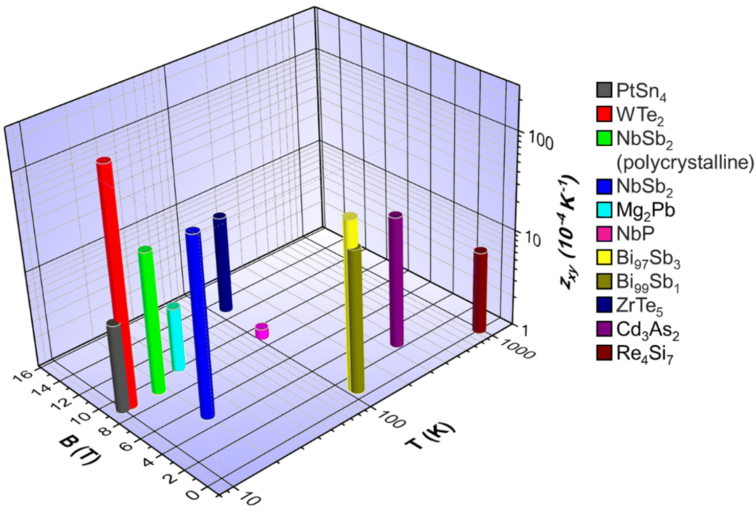 | ||
| Fig. 8 Plot of the peak transverse figure-of-merit (zxy) as a function of the optimum temperature (T) and magnetic field strength (B) for PtSn4,168 WTe2,169 NbSb2,170 polycrystalline NbSb2,171 Mg2Pb,172 NbP,173 Bi97Sb3,167 Bi99Sb1,174 ZrTe5,175 Cd3As2,162 and Re4Si7.153 All properties plotted are based on the single-crystalline materials, unless otherwise stated. | ||
5. Conclusion and prospects
A few decades ago in TE materials research, most studies reported the peak zT of the material, which usually occurs at the highest measured temperature. As the research on TE materials advanced over the years, many effective strategies and paradigms have been explored and developed to not only enhance the peak zT but also the average zT over a wide temperature gradient (from room temperature to the highest measured temperature). Such strategies include band convergence,8,43–51 resonant levels,52–58 all-scale hierarchal defect architectures,59–65 off-centred and discordant atoms,66–68 metavalent bonding,69–74 minority carrier blocking additives,75–78 and wide band-gap and layered structures.10,79–84 While there has been a general push in recent years to enhance the average zT, perhaps for the plasma-facing applications, with a useful temperature range of 973–1273 K or above, it would be more feasible to revert back to the old focus of enhancing peak zT at the highest temperature as the minimum cold side temperature is still rather high (∼973 K). The paradigm shifts in the TE material development caused by the pioneering discoveries by Dresselhaus and Kanatzidis of lattice thermal conductivity reduction through nano-structuring and all-scale hierarchical defect architectures respectively,176,177 may also be potentially reversed with the possible preference for high power factor TE materials (over high zT materials), to accommodate the compromise in TE device design with efficient heat dissipation from the armour layer.In summary, in terms of overall suitability for TE devices to harvest heat from plasma-facing surfaces in a fusion reactor, considering the expected TE performance and service stability, Si1−xGex-based materials may be the most suitable. The p-type Si0.8Ge0.2 + 6 wt% Y2O3 and n-type Si0.8Ge0.2 + 0.23 vol% SiC nanocomposites, with a high zT of 1.81 at 1100 K and 1.70 at 1173 K, respectively,64,71 are especially promising due to the absence of very high-activating elements and the presence of nanoprecipitates that not only enhance the TE performance but also the neutron irradiation damage resistance by potentially partitioning a high density of He nano-bubbles which effectively promotes recombination of void swelling-causing defects. To minimise material costs, it may be better to reduce the Ge content in Si1−xGex-based materials, especially when thermal conductivities need not be minimized as much as possible to allow more heat dissipation from the armour layer.
Given the extremely high temperatures of the plasma in the fusion reactor (∼1.5 × 10⁸ K), it is theoretically possible to extract heat at temperatures far higher than 1273 K for a higher power conversion efficiency, but current reactors are limited by the safe working temperature range of the armour materials. With the ideal working temperature range of W being 873–1673 K,8 it was assumed that an average temperature of 1273 K would be the ideal base temperature for normal operations, providing a safe allowance from the upper limit in case of instabilities in the plasma. Recently, there have been a couple of breakthroughs in improving plasma stabilities, such as tailoring the plasma error fields to minimize ELMs with little degradation to the magnetic confinement,178 negative triangularity shaping of the plasma to suppress ELMs,179 an AI model to predict “tearing mode” plasma instabilities so that the operating conditions can be adjusted to prevent them from happening,180 the demonstration of stable tokamak plasmas with line-averaged density approximately 20% above the empirical limit,181 and the tungsten environment in a steady-state tokamak (WEST) sustaining the plasma for a record-breaking duration of 6 min.182 Therefore, with the advances in plasma stabilities, less safety allowance may be required so that the fusion reactor may be allowed to operate with the plasma-facing surfaces at higher temperatures for improved conversion efficiencies. This may require the use of TE materials that can operate at temperatures higher than 1273 K.
As such TE properties above 1273 K are not commonly reported, newer TE materials with promising zTs at lower temperatures can be screened for much higher temperature applications based on the limits imposed by their thermal stabilities and their bandgaps (Eg). The maximum operating temperatures of longitudinal TE materials are limited by their Eg because of the detrimental bipolar effect, where the high temperatures may provide enough energy for free minority carriers to be excited across the Eg, lowering the performances of longitudinal TE materials which rely on majority carrier transport. Most good TE semiconductor materials seem to follow an approximate trend of Eg/(kB·Tmax) ≈ 5 to 10, where kB is the Boltzmann constant and Tmax is the maximum operating temperature.183–185 Using this as a rough screening guide, p-type B4C may potentially be able to operate up to ∼2425 K without experiencing bipolar conduction, due to its wide Eg of 2.09 eV and high melting point of 2620 K.186 While n-type SrB6 also has a high melting point of 2235 K, its maximum operating temperature may be limited to 1334 K due to its narrower Eg of 1.15 eV.187 However, bipolar conduction is not a limiting factor for transverse TE materials which use both electrons and holes within the same material, such as the narrow-gap Re4Si7 (Eg of 0.12 eV),153 which would have been a highly promising material for plasma-facing transverse TE devices, if not for its single-crystalline nature and the presence of high-activating Re.
Overall, as the global attention on nuclear fusion energy grows, detailed studies on these promising high temperature TE materials and their service stabilities in a high radiation dose environment will be a highly valued direction in the future. With the continued development of improved fusion reactor designs and structural materials, more opportunities for TE material applications are bound to open up, catalysing the advancement of TE material development for applications under extreme conditions.
Data availability
No primary research results, software or code have been included and no new data were generated or analysed as part of this review.Author contributions
Conceptualization: X. Y. T. and A. C. Y. N., manuscript preparation: X. Y. T., H. L. and J. D., and supervision and review: J. C., A. C. Y. N., and A. S.Conflicts of interest
There are no conflicts of interest to declare.Acknowledgements
X. Y. T., J. C. and A. S. acknowledge support by the Agency for Science, Technology and Research (A*STAR) e-Asia Joint Research Program award no. R22I1IR0053. J. C. acknowledges support by the A*STAR Singapore Career Development Fund (CDF) C222812009. The authors would also like to acknowledge Na Gong, Baisong Cheng and Shijie Wang for the consultations which were beneficial to this review.References
- J. P. Holdren, D. H. Berwald, R. J. Budnitz, J. G. Crocker, J. G. Delene, R. D. Endicott, M. S. Kazimi, R. A. Krakowski, B. G. Logan and K. R. Schultz, Fusion Technol., 1988, 13, 7–56 CrossRef CAS.
- T. E. G. Nicholas, T. P. Davis, F. Federici, J. Leland, B. S. Patel, C. Vincent and S. H. Ward, Energy Policy, 2021, 149, 112043 CrossRef.
- S. Kousik Suraparaju, M. Samykano, S. Namasivayam, K. Kadirgama and D. Ramasamy, E3S Web Conf., 2024, 488, 02006 CrossRef.
- L.-l. Zou, X. Chen, Y.-t. Wu, X. Wang and C.-f. Ma, Sol. Energy Mater. Sol. Cells, 2019, 190, 12–19 CrossRef CAS.
- J. Raade and B. Elkin, US Pat., US20130180520A1, 2013 Search PubMed.
- Y. Ahn, S. J. Bae, M. Kim, S. K. Cho, S. Baik, J. I. Lee and J. E. Cha, Nucl. Eng. Technol., 2015, 47, 647–661 CrossRef.
- C. Baus, P. Barron, A. D'Angiò, Y. Hirata, S. Konishi, J. Mund, T. Nagao, D. Nakahara, R. Pearson, M. Sakaguchi, K. Sakamoto, K. Seko, S. Takeda, A. Wilson and Y. Yoshioka, J. Fusion Energy, 2023, 42, 10 CrossRef CAS.
- J. Linke, J. Du, T. Loewenhoff, G. Pintsuk, B. Spilker, I. Steudel and M. Wirtz, Matter Radiat. Extremes, 2019, 4, 056201 CrossRef.
- H. Liu, C. K. I. Tan, T. L. Meng, M. Lin, C. J. Lee, J. Liu, Z. Zhang, D. C. Tan, J. Cao and A. Suwardi, J. Mater. Process. Technol., 2022, 301, 117440 CrossRef CAS.
- S. J. Zinkle and L. L. Snead, Annu. Rev. Mater. Res., 2014, 44, 241–267 CrossRef CAS.
- U. A. E. Authority, UK Fusion Materials Roadmap 2021–2040, The Henry Royce Institute, United Kingdom, 2021 Search PubMed.
- T. Caillat and J. Yang, MRS Bull., 2011, 31, 224–229 Search PubMed.
- B. Jiang, W. Wang, S. Liu, Y. Wang, C. Wang, Y. Chen, L. Xie, M. Huang and J. He, Science, 2022, 377, 208–213 CrossRef CAS PubMed.
- C. Xu, Z. Liang, W. Ren, S. Song, F. Zhang and Z. Ren, Adv. Energy Mater., 2022, 2202392 CrossRef CAS.
- B. Jiang, Y. Yu, J. Cui, X. Liu, L. Xie, J. Liao, Q. Zhang, Y. Huang, S. Ning, B. Jia, B. Zhu, S. Bai, L. Chen, S. J. Pennycook and J. He, Science, 2021, 371, 830–834 CrossRef CAS PubMed.
- X. Hu, P. Jood, M. Ohta, M. Kunii, K. Nagase, H. Nishiate, M. G. Kanatzidis and A. Yamamoto, Energy Environ. Sci., 2016, 9, 517–529 RSC.
- P. Jood, M. Ohta, A. Yamamoto and M. G. Kanatzidis, Joule, 2018, 2, 1339–1355 CrossRef CAS.
- J. Cao, X. Y. Tan, J. Dong, H. Liu, Y. Zheng, Q. Zhu, J. Xu, G. Zhang, J. Wu and A. Suwardi, Mater. Today Phys., 2023, 34, 101071 CrossRef CAS.
- N. Jia, J. Cao, X. Y. Tan, J. Dong, H. Liu, C. K. I. Tan, J. Xu, Q. Yan, X. J. Loh and A. Suwardi, Mater. Today Phys., 2021, 21, 100519 CrossRef CAS.
- A. Shakouri, Annu. Rev. Mater. Res., 2011, 41, 399–431 CrossRef CAS.
- B. Cook, Energies, 2022, 15(8), 2957 CrossRef CAS.
- S. Yamaguchi, K. Ikeda, H. Nakamura, K. Kuroda and O. Motojima, Fusion Eng. Des., 1998, 41, 555–559 CrossRef CAS.
- J. Dong, Y. Jiang, J. Liu, J. Pei, X. Y. Tan, H. Hu, A. Suwardi, N. Jia, C. Liu, Q. Zhu, Q. Yan and J.-F. Li, Nano Energy, 2022, 103, 107809 CrossRef CAS.
- Y. Jiang, J. Dong, H.-L. Zhuang, J. Yu, B. Su, H. Li, J. Pei, F.-H. Sun, M. Zhou, H. Hu, J.-W. Li, Z. Han, B.-P. Zhang, T. Mori and J.-F. Li, Nat. Commun., 2022, 13, 6087 CrossRef CAS PubMed.
- J. Pei, J.-L. Shi, H. Li, Y. Jiang, J. Dong, H.-L. Zhuang, B. Cai, B. Su, J. Yu, W. Zhou, B.-P. Zhang and J.-F. Li, Adv. Funct. Mater., 2023, 2214771 CrossRef CAS.
- J. Dong, Y. Jiang, Y. Sun, J. Liu, J. Pei, W. Li, X. Y. Tan, L. Hu, N. Jia, B. Xu, Q. Li, J.-F. Li, Q. Yan and M. G. Kanatzidis, J. Am. Chem. Soc., 2023, 145, 1988–1996 CrossRef CAS PubMed.
- J. Cao, X. Y. Tan, N. Jia, D. Lan, S. F. D. Solco, K. Chen, S. W. Chien, H. Liu, C. K. I. Tan, Q. Zhu, J. Xu, Q. Yan and A. Suwardi, Nanoscale, 2022, 14, 410–418 RSC.
- J. Dong, L. Hu, J. Liu, Y. Liu, Y. Jiang, Z. Yu, X. Y. Tan, A. Suwardi, Q. Zheng and Q. Li, Adv. Funct. Mater., 2024, 2314499 CrossRef CAS.
- J. Cao, X. Y. Tan, N. Jia, D. Lan, S. F. D. Solco, K. Chen, S. W. Chien, H. Liu, C. K. I. Tan and Q. Zhu, Nanoscale, 2022, 14, 410–418 RSC.
- J. Cao, S. W. Chien, X. Y. Tan, C. K. I. Tan, Q. Zhu, J. Wu, X. Wang, Y. Zhao, L. Yang, Q. Yan, H. Liu, J. Xu and A. Suwardi, ChemNanoMat, 2021, 7, 476–482 CrossRef CAS.
- N. Jia, J. Cao, X. Y. Tan, J. Zheng, S. W. Chien, L. Yang, K. Chen, H. K. Ng, S. S. F. Duran and H. Liu, J. Mater. Chem. A, 2021, 9, 23335–23344 RSC.
- A. Suwardi, J. Cao, Y. Zhao, J. Wu, S. W. Chien, X. Y. Tan, L. Hu, X. Wang, W. Wang and D. Li, Mater. Today Phys., 2020, 14, 100239 CrossRef.
- A. Suwardi, S. H. Lim, Y. Zheng, X. Wang, S. W. Chien, X. Y. Tan, Q. Zhu, L. M. N. Wong, J. Cao, W. Wang, Q. Yan, C. K. I. Tan and J. Xu, J. Mater. Chem. C, 2020, 8, 16940–16948 RSC.
- A. Suwardi, J. Cao, L. Hu, F. Wei, J. Wu, Y. Zhao, S. H. Lim, L. Yang, X. Y. Tan, S. W. Chien, Y. Yin, W.-X. Zhou, W. L. Mun Nancy, X. Wang, S. H. Lim, X. Ni, D. Li, Q. Yan, Y. Zheng, G. Zhang and J. Xu, J. Mater. Chem. A, 2020, 8, 18880–18890 RSC.
- J. P. Heremans, V. Jovovic, E. S. Toberer, A. Saramat, K. Kurosaki, A. Charoenphakdee, S. Yamanaka and G. J. Snyder, Science, 2008, 321, 554–557 CrossRef CAS.
- Z. Chen, Z. Jian, W. Li, Y. Chang, B. Ge, R. Hanus, J. Yang, Y. Chen, M. Huang, G. J. Snyder and Y. Pei, Adv. Mater., 2017, 29, 1606768 CrossRef PubMed.
- Z.-Z. Luo, S. Cai, S. Hao, T. P. Bailey, X. Su, I. Spanopoulos, I. Hadar, G. Tan, Y. Luo, J. Xu, C. Uher, C. Wolverton, V. P. Dravid, Q. Yan and M. G. Kanatzidis, J. Am. Chem. Soc., 2019, 141, 16169–16177 CrossRef CAS.
- Y. Wu, P. Nan, Z. Chen, Z. Zeng, R. Liu, H. Dong, L. Xie, Y. Xiao, Z. Chen, H. Gu, W. Li, Y. Chen, B. Ge and Y. Pei, Advanced Science, 2020, 7, 1902628 CrossRef CAS.
- Y. Xiao, Y. Wu, P. Nan, H. Dong, Z. Chen, Z. Chen, H. Gu, B. Ge, W. Li and Y. Pei, Chem, 2020, 6, 523–537 CAS.
- L.-D. Zhao, S.-H. Lo, Y. Zhang, H. Sun, G. Tan, C. Uher, C. Wolverton, V. P. Dravid and M. G. Kanatzidis, Nature, 2014, 508, 373–377 CrossRef CAS PubMed.
- C. Chang, M. Wu, D. He, Y. Pei, C.-F. Wu, X. Wu, H. Yu, F. Zhu, K. Wang, Y. Chen, L. Huang, J.-F. Li, J. He and L.-D. Zhao, Science, 2018, 360, 778–783 CrossRef CAS.
- Y. K. Lee, Z. Luo, S. P. Cho, M. G. Kanatzidis and I. Chung, Joule, 2019, 3, 719–731 CrossRef CAS.
- B. Qin, D. Wang, X. Liu, Y. Qin, J.-F. Dong, J. Luo, J.-W. Li, W. Liu, G. Tan, X. Tang, J.-F. Li, J. He and L.-D. Zhao, Science, 2021, 373, 556–561 CrossRef CAS.
- D. Liu, D. Wang, T. Hong, Z. Wang, Y. Wang, Y. Qin, L. Su, T. Yang, X. Gao, Z. Ge, B. Qin and L.-D. Zhao, Science, 2023, 380, 841–846 CrossRef CAS.
- D. Zhang, M. Xie, D. Safanama, K. Saglik, X. Y. Tan, S. F. D. Solco, J. Cao, C. K. I. Tan, H. Liu and S. Wang, Adv. Energy Sustainability Res., 2023, 4, 2300069 CrossRef CAS.
- J. Dong, D. Zhang, J. Liu, Y. Jiang, X. Y. Tan, N. Jia, J. Cao, A. Suwardi, Q. Zhu and J. Xu, Inorg. Chem., 2023, 62, 17905–17912 CrossRef CAS PubMed.
- J. Cao, J. Dong, K. Saglik, D. Zhang, S. F. D. Solco, I. J. W. J. You, H. Liu, Q. Zhu, J. Xu, J. Wu, F. Wei, Q. Yan and A. Suwardi, Nano Energy, 2023, 107, 108118 CrossRef CAS.
- Z. Gong, K. Saglik, J. Wu, A. Suwardi and J. Cao, Nanoscale, 2023, 15, 18283–18290 RSC.
- J. Cao, Y. Sim, X. Y. Tan, J. Zheng, S. W. Chien, N. Jia, K. Chen, Y. B. Tay, J. F. Dong and L. Yang, Adv. Mater., 2022, 34, 2110518 CrossRef CAS PubMed.
- J. Cao, J. Zheng, H. Liu, C. K. I. Tan, X. Wang, W. Wang, Q. Zhu, Z. Li, G. Zhang, J. Wu, L. Zhang, J. Xu and A. Suwardi, Mater. Today Energy, 2022, 25, 100964 CrossRef CAS.
- J. Zheng, S. F. D. Solco, C. J. E. Wong, S. A. Sia, X. Y. Tan, J. Cao, J. C. C. Yeo, W. Yan, Q. Zhu and Q. Yan, J. Mater. Chem. A, 2022, 10, 19787–19796 RSC.
- Y. Zheng, H. Xie, Q. Zhang, A. Suwardi, X. Cheng, Y. Zhang, W. Shu, X. Wan, Z. Yang and Z. Liu, ACS Appl. Mater. Interfaces, 2020, 12, 36186–36195 CrossRef CAS.
- X. Y. Tan, J. Dong, J. Liu, D. Zhang, S. F. D. Solco, K. Sağlık, N. Jia, I. J. W. J. You, S. W. Chien, X. Wang, L. Hu, Y. Luo, Y. Zheng, D. X. Y. Soo, R. Ji, K. C. H. Goh, Y. Jiang, J.-F. Li, A. Suwardi, Q. Zhu, J. Xu and Q. Yan, Advanced Science, 2024, 2400870 CrossRef CAS.
- D. F. Woerner, Next-Generation RTG Study Final Report 2017, N. Jet Propulsion Laboratory Report JPL D-99657, Jet Propulsion Laboratory, NASA, Pasadena, California, 2017 Search PubMed.
- S. I. Kim, K. H. Lee, H. A. Mun, H. S. Kim, S. W. Hwang, J. W. Roh, D. J. Yang, W. H. Shin, X. S. Li, Y. H. Lee, G. J. Snyder and S. W. Kim, Science, 2015, 348, 109 CrossRef CAS.
- B. Zhu, X. Liu, Q. Wang, Y. Qiu, Z. Shu, Z. Guo, Y. Tong, J. Cui, M. Gu and J. He, Energy Environ. Sci., 2020, 13, 2106–2114 RSC.
- F. Zhang, C. Chen, H. Yao, F. Bai, L. Yin, X. Li, S. Li, W. Xue, Y. Wang, F. Cao, X. Liu, J. Sui and Q. Zhang, Adv. Funct. Mater., 2020, 30, 1906143 CrossRef CAS.
- H. Zhao, J. Sui, Z. Tang, Y. Lan, Q. Jie, D. Kraemer, K. McEnaney, A. Guloy, G. Chen and Z. Ren, Nano Energy, 2014, 7, 97–103 CrossRef CAS.
- Y.-F. Tsai, P.-C. Wei, L. Chang, K.-K. Wang, C.-C. Yang, Y.-C. Lai, C.-R. Hsing, C.-M. Wei, J. He, G. J. Snyder and H.-J. Wu, Adv. Mater., 2021, 33, 2005612 CrossRef CAS PubMed.
- L. Fu, M. Yin, D. Wu, W. Li, D. Feng, L. Huang and J. He, Energy Environ. Sci., 2017, 10, 2030–2040 RSC.
- J. Yu, C. Fu, Y. Liu, K. Xia, U. Aydemir, T. C. Chasapis, G. J. Snyder, X. Zhao and T. Zhu, Adv. Energy Mater., 2018, 8, 1701313 CrossRef.
- Y. Liu, H. Xie, C. Fu, G. J. Snyder, X. Zhao and T. Zhu, J. Mater. Chem. A, 2015, 3, 22716–22722 RSC.
- M. Bouchacourt and F. Thevenot, J. Mater. Sci., 1985, 20, 1237–1247 CrossRef CAS.
- S. Ahmad, A. Singh, A. Bohra, R. Basu, S. Bhattacharya, R. Bhatt, K. N. Meshram, M. Roy, S. K. Sarkar, Y. Hayakawa, A. K. Debnath, D. K. Aswal and S. K. Gupta, Nano Energy, 2016, 27, 282–297 CrossRef CAS.
- R. Basu, S. Bhattacharya, R. Bhatt, M. Roy, S. Ahmad, A. Singh, M. Navaneethan, Y. Hayakawa, D. K. Aswal and S. K. Gupta, J. Mater. Chem. A, 2014, 2, 6922–6930 RSC.
- C. J. Perez, M. Wood, F. Ricci, G. Yu, T. Vo, S. K. Bux, G. Hautier, G.-M. Rignanese, G. J. Snyder and S. M. Kauzlarich, Sci. Adv., 2021, 7, eabe9439 CrossRef CAS PubMed.
- J. M. Ma, S. M. Clarke, W. G. Zeier, T. Vo, P. Von Allmen, G. Jeffrey Snyder, R. B. Kaner, J.-P. Fleurial and S. K. Bux, J. Mater. Chem. C, 2015, 3, 10459–10466 RSC.
- D. Cheikh, B. E. Hogan, T. Vo, P. Von Allmen, K. Lee, D. M. Smiadak, A. Zevalkink, B. S. Dunn, J.-P. Fleurial and S. K. Bux, Joule, 2018, 2, 698–709 CrossRef CAS.
- T. Zhu, G. Yu, J. Xu, H. Wu, C. Fu, X. Liu, J. He and X. Zhao, Adv. Electron. Mater., 2016, 2, 1600171 CrossRef.
- X. W. Wang, H. Lee, Y. C. Lan, G. H. Zhu, G. Joshi, D. Z. Wang, J. Yang, A. J. Muto, M. Y. Tang, J. Klatsky, S. Song, M. S. Dresselhaus, G. Chen and Z. F. Ren, Appl. Phys. Lett., 2008, 93, 193121 CrossRef.
- S. Bathula, M. Jayasimhadri, B. Gahtori, A. Kumar, A. K. Srivastava and A. Dhar, Phys. Chem. Chem. Phys., 2017, 19, 25180–25185 RSC.
- M. Zebarjadi, G. Joshi, G. Zhu, B. Yu, A. Minnich, Y. Lan, X. Wang, M. Dresselhaus, Z. Ren and G. Chen, Nano Lett., 2011, 11, 2225–2230 CrossRef CAS.
- A. F. May, J.-P. Fleurial and G. J. Snyder, Phys. Rev. B: Condens. Matter Mater. Phys., 2008, 78, 125205 CrossRef.
- S. R. Brown, S. M. Kauzlarich, F. Gascoin and G. J. Snyder, Chem. Mater., 2006, 18, 1873–1877 CrossRef CAS.
- C. Wood, AIP Conf. Proc., 1986, 140, 362–372 CrossRef CAS.
- J.-L. Innocent, D. Portehault, G. Gouget, S. Maruyama, I. Ohkubo and T. Mori, Mater. Renew. Sustain. Energy, 2017, 6, 6 CrossRef.
- M. Takeda, T. Fukuda and T. Miura, 2002.
- R. W. Olesinski and G. J. Abbaschian, Bull. Alloy Phase Diagrams, 1984, 5, 180–183 CrossRef CAS.
- C. E. Kelley, R. L. Wiley and R. Lorentzen, Thermal Performance of Foil Insulated SiGe Converters, American Inst of Aeronautics and Astronautics, United States, 1973 Search PubMed.
- J. F. Nakahara, B. Franklin and L. E. DeFillipo, AIP Conf. Proc., 1995, 324, 809–814 CrossRef CAS.
- S. F. D. Solco, X. Y. Tan, D. Zhang, J. Cao, X. Wang, Q. Zhu, S. Wang, L. T. Chew, H. Liu, C. K. I. Tan, J. Wu, D. C. C. Tan, J. Xu and A. Suwardi, J. Mater. Sci., 2022, 57, 20299–20308 CrossRef CAS.
- R. C. o. America, Optimization of Silicon–Germanium Thermoelectric Modules for Transportation Corps Silent Boat Design, D. E. C. Department, U.S. Army Transportation Research Command, Harrison, NJ, 1963 Search PubMed.
- J. Garg, N. Bonini, B. Kozinsky and N. Marzari, Phys. Rev. Lett., 2011, 106, 045901 CrossRef PubMed.
- J. Cao, Y. Sim, X. Y. Tan, J. Zheng, S. W. Chien, N. Jia, K. Chen, Y. B. Tay, J.-F. Dong, L. Yang, H. K. Ng, H. Liu, C. K. I. Tan, G. Xie, Q. Zhu, Z. Li, G. Zhang, L. Hu, Y. Zheng, J. Xu, Q. Yan, X. J. Loh, N. Mathews, J. Wu and A. Suwardi, Adv. Mater., 2022, 34, 2110518 CrossRef CAS PubMed.
- B. Qiu, Z. Tian, A. Vallabhaneni, B. Liao, J. M. Mendoza, O. D. Restrepo, X. Ruan and G. Chen, Europhys. Lett., 2015, 109, 57006 CrossRef.
- A. P. Justl and S. M. Kauzlarich, ACS Appl. Mater. Interfaces, 2022, 14, 47246–47254 CrossRef CAS PubMed.
- C. Wood, MRS Online Proc. Libr., 1987, 97, 335–346 CrossRef CAS.
- J. Li, R. Liu, Q. Song, Z. Gao, H. Huang, Q. Zhang, X. Shi, S. Bai and L. Chen, Acta Mater., 2022, 224, 117526 CrossRef CAS.
- E. S. Toberer, A. Zevalkink and G. J. Snyder, J. Mater. Chem., 2011, 21, 15843–15852 RSC.
- K. Saglik, J. Dong, D. Zhang, T. Z. Hsu, S. S. F. Duran, J. Cao, Q. Zhu, R. Ji, W. S. Kai and T. S. Lang, J. Solid State Chem., 2024, 124642 CrossRef CAS.
- S. Yamaguchi, A. Sagara, A. Komori, T. Tazima, O. Motojima, A. Iiyoshi, K. Matsubara, M. Onozuka, K. Koganezawa and T. Matsuda, Thermoelectric conversion at the divertor plates and the first wall of a fusion reactor, Fusion technology, 1994: Proceedings, Karlsruhe, Germany, vol. 1, 1995 Search PubMed.
- V. Domnich, S. Reynaud, R. A. Haber and M. Chhowalla, J. Am. Ceram. Soc., 2011, 94, 3605–3628 CrossRef CAS.
- K. Saglik, B. Mete, I. Terzi, C. Candolfi and U. Aydemir, Adv. Phys. Res., 2023, 2, 2300010 CrossRef.
- J. Cao, T. L. Meng, X. Zhang, N. Gong, R. Karyappa, C. K. I. Tan, A. Suwardi, Q. Zhu and H. Liu, World Sci. Annu. Rev. Funct. Mater., 2023, 1, 2230005 CrossRef.
- J. Cao, T. L. Meng, X. Zhang, C. K. I. Tan, A. Suwardi and H. Liu, Mater. Today Electron., 2022, 2, 100005 CrossRef.
- F.-D. Börner, M. Schreier, B. Feng, W. Lippmann, H.-P. Martin, A. Michaelis and A. Hurtado, J. Mater. Res., 2014, 29, 1771–1780 CrossRef.
- A. Prytuliak, S. Maruyama and T. Mori, Mater. Res. Bull., 2013, 48, 1972–1977 CrossRef CAS.
- R. He, D. Kraemer, J. Mao, L. Zeng, Q. Jie, Y. Lan, C. Li, J. Shuai, H. S. Kim, Y. Liu, D. Broido, C.-W. Chu, G. Chen and Z. Ren, Proc. Natl. Acad. Sci. U. S. A., 2016, 113, 13576–13581 CrossRef CAS.
- J. Zhou, H. Zhu, T.-H. Liu, Q. Song, R. He, J. Mao, Z. Liu, W. Ren, B. Liao, D. J. Singh, Z. Ren and G. Chen, Nat. Commun., 2018, 9, 1721 CrossRef.
- Z. Huang, L. Yin, C. Hu, J. Shen, T. Zhu, Q. Zhang, K. Xia, J. Xin and X. Zhao, J. Mater. Sci. Technol, 2020, 40, 113–118 CrossRef CAS.
- G. Rogl, A. Grytsiv, M. Gürth, A. Tavassoli, C. Ebner, A. Wünschek, S. Puchegger, V. Soprunyuk, W. Schranz, E. Bauer, H. Müller, M. Zehetbauer and P. Rogl, Acta Mater., 2016, 107, 178–195 CrossRef CAS.
- W. Y. S. Lim, D. Zhang, S. S. F. Duran, X. Y. Tan, C. K. I. Tan, J. Xu and A. Suwardi, Front. Mater., 2021, 8, 745698 CrossRef.
- R. Chen, H. Kang, R. Min, Z. Chen, E. Guo, X. Yang and T. Wang, Int. Mater. Rev., 2024, 69, 83–106 CrossRef CAS.
- N. Kempf, C. Karthik, B. J. Jaques, J. Gigax, L. Shao, D. P. Butt, R. He, D. Wang, Z. Ren and Y. Zhang, Appl. Phys. Lett., 2018, 112, 243902 CrossRef.
- M. Miyamoto, S. Mikami, H. Nagashima, N. Iijima, D. Nishijima, R. P. Doerner, N. Yoshida, H. Watanabe, Y. Ueda and A. Sagara, J. Nucl. Mater., 2015, 463, 333–336 CrossRef CAS.
- M. J. Baldwin, R. P. Doerner, W. R. Wampler, D. Nishijima, T. Lynch and M. Miyamoto, Nucl. Fusion, 2011, 51, 103021 CrossRef.
- N. Gong, R. Karyappa, T. L. Meng, Y. Wang, S. L. Teo, J. Cao, M. Lin, X. Huang, C. K. I. Tan and A. Suwardi, J. Mater. Sci., 2023, 58, 12058–12069 CrossRef CAS.
- N. Gong, H. L. Seng, H. Jin, J. Cao, T. L. Meng, S. L. Teo, R. Karyappa, X. Zhang, L. Zhang and M. Lin, Mater. Today Commun., 2023, 34, 105050 CrossRef CAS.
- W. Liu, Q. Jie, H. S. Kim and Z. Ren, Acta Mater., 2015, 87, 357–376 CrossRef CAS.
- G. De Temmerman, in Wiley Encyclopedia of Composites, 2012, pp. 1–9, DOI:10.1002/9781118097298.weoc047.
- T. Koyanagi, Y. Katoh, T. Nozawa, L. L. Snead, S. Kondo, C. H. Henager, M. Ferraris, T. Hinoki and Q. Huang, J. Nucl. Mater., 2018, 511, 544–555 CrossRef CAS.
- P. Qiu, J. Cheng, J. Chai, X. Du, X. Xia, C. Ming, C. Zhu, J. Yang, Y.-Y. Sun, F. Xu, X. Shi and L. Chen, Adv. Energy Mater., 2022, 12, 2200247 CrossRef CAS.
- J. Cao, B. Yuan, N. Gong, T. L. Meng, S. L. Teo, A. M. Yong, X. Zhang, M. Lin, R. Karyappa and L. Zhang, Appl. Surf. Sci., 2023, 611, 155700 CrossRef CAS.
- R. S. S. Maki, F. Muhammad, J. Maletaskic, A. V. Gubarevich, K. Yoshida, T. Yano, T. S. Suzuki and T. Uchikoshi, J. Asian Ceram. Soc., 2022, 10, 370–377 CrossRef.
- Y. Katsuda, P. Gerstel, J. Narayanan, J. Bill and F. Aldinger, J. Eur. Ceram. Soc., 2006, 26, 3399–3405 CrossRef CAS.
- G. B. Yadhukulakrishnan, A. Rahman, S. Karumuri, M. M. Stackpoole, A. K. Kalkan, R. P. Singh and S. P. Harimkar, Mater. Sci. Eng., A, 2012, 552, 125–133 CrossRef CAS.
- C. S. Chua, S. Y. Ow, S. L. Liew, J. Liu, C. B. Soh, L. Shen and S. Wang, Adv. Appl. Ceram., 2022, 121, 46–51 CrossRef CAS.
- M. Humenik Jr and W. D. Kingery, J. Am. Ceram. Soc., 1954, 37, 18–23 CrossRef.
- S. J. Zinkle and J. T. Busby, Mater. Today, 2009, 12, 12–19 CrossRef CAS.
- M. J. Gorley, Mater. Sci. Technol., 2015, 31, 975–980 CrossRef CAS.
- S. J. Piet, E. T. Cheng, S. Fetter and J. S. Herring, Fusion Technol., 1991, 19, 146–161 CrossRef CAS.
- D. J. Ward and S. L. Dudarev, Mater. Today, 2008, 11, 46–53 CrossRef CAS.
- S. Tanaka, K. Okuno, Y. Takeuchi and T. Tabara, Appl. Radiat. Isot., 2022, 181, 110074 CrossRef CAS PubMed.
- Y. Katoh, K. Ozawa, C. Shih, T. Nozawa, R. J. Shinavski, A. Hasegawa and L. L. Snead, J. Nucl. Mater., 2014, 448, 448–476 CrossRef CAS.
- S. Agarwal, T. Koyanagi, A. Bhattacharya, L. Wang, Y. Katoh, X. Hu, M. Pagan and S. J. Zinkle, Acta Mater., 2020, 186, 1–10 CrossRef CAS.
- F. Thévenot, J. Eur. Ceram. Soc., 1990, 6, 205–225 CrossRef.
- M. Tchonang Pokaha and D. E. Serfontein, J. Nucl. Sci. Technol., 2018, 55, 843–849 CrossRef CAS.
- L. L. Snead, T. Nozawa, M. Ferraris, Y. Katoh, R. Shinavski and M. Sawan, J. Nucl. Mater., 2011, 417, 330–339 CrossRef CAS.
- N. Gong, T. L. Meng, S. L. Teo, J. Cao, C. J. Lee, C. K. I. Tan, D. C. Tan, A. Suwardi, M. Lin and R. Misra, Corros. Sci., 2023, 214, 111026 CrossRef CAS.
- G. D. Watkins, Mater. Sci. Semicond. Process., 2000, 3, 227–235 CrossRef CAS.
- K. E. Sickafus, in Comprehensive Nuclear Materials, ed. R. J. M. Konings, Elsevier, Oxford, 2012, pp. 123–139, DOI:10.1016/B978-0-08-056033-5.00005-7.
- Y. Dai, G. R. Odette and T. Yamamoto, in Comprehensive Nuclear Materials, ed. R. J. M. Konings, Elsevier, Oxford, 2012, pp. 141–193, DOI:10.1016/B978-0-08-056033-5.00006-9.
- N. H. Packan and K. Farrell, J. Nucl. Mater., 1979, 85–86, 677–681 CrossRef CAS.
- N. Gong, H. Seet, J. Cao, T. L. Meng, Y. Wang, D. C. Tan, C. K. I. Tan, A. Suwardi, Q. Zhu and D. J. Blackwood, Mater. Lett., 2023, 331, 133434 CrossRef CAS.
- M. K. Miller, D. T. Hoelzer, E. A. Kenik and K. F. Russell, J. Nucl. Mater., 2004, 329–333, 338–341 CrossRef.
- T. Yamamoto, G. R. Odette, P. Miao, D. T. Hoelzer, J. Bentley, N. Hashimoto, H. Tanigawa and R. J. Kurtz, J. Nucl. Mater., 2007, 367–370, 399–410 CrossRef CAS.
- K. M. Tynyshbayeva, A. L. Kozlovskiy, R. V. Rakhimov, V. V. Uglov and M. V. Zdorovets, Materials, 2023, 16(17), 5750 CrossRef CAS.
- D. Zhang, J. Ramiah, M. Cagirici, K. Saglik, S. F. D. Solco, J. Cao, J. Xu and A. Suwardi, Mater. Horiz., 2024, 11, 847–854 RSC.
- W. Y. S. Lim, J. Cao, A. Suwardi, T. L. Meng, C. K. I. Tan and H. Liu, J. Adhes. Sci. Technol., 2022, 36, 2482–2504 CrossRef CAS.
- D. Zhang, W. Y. S. Lim, S. S. F. Duran, X. J. Loh and A. Suwardi, ACS Energy Lett., 2022, 7, 720–735 CrossRef CAS.
- D. Zhang, X. J. G. Lim, X. Li, K. Saglik, S. F. D. Solco, X. Y. Tan, Y. Leow, W. Zhai, C. K. I. Tan, J. Xu and A. Suwardi, ACS Energy Lett., 2023, 8, 332–338 CrossRef CAS.
- Y. Zheng, T. J. Slade, L. Hu, X. Y. Tan, Y. Luo, Z.-Z. Luo, J. Xu, Q. Yan and M. G. Kanatzidis, Chem. Soc. Rev., 2021, 50, 9022–9054 RSC.
- H. Xiang, Y. Xing, F.-z. Dai, H. Wang, L. Su, L. Miao, G. Zhang, Y. Wang, X. Qi, L. Yao, H. Wang, B. Zhao, J. Li and Y. Zhou, J. Adv. Ceram., 2021, 10, 385–441 CrossRef CAS.
- R. A. Kishore, A. Nozariasbmarz, B. Poudel, M. Sanghadasa and S. Priya, Nat. Commun., 2019, 10, 1765 CrossRef PubMed.
- R. Freer and A. V. Powell, J. Mater. Chem. C, 2020, 8, 441–463 RSC.
- M. Wolf, R. Hinterding and A. Feldhoff, Entropy, 2019, 21(11), 1058 CrossRef CAS.
- D. Narducci, Appl. Phys. Lett., 2011, 99, 102104 CrossRef.
- S. LeBlanc, S. K. Yee, M. L. Scullin, C. Dames and K. E. Goodson, Renewable Sustainable Energy Rev., 2014, 32, 313–327 CrossRef CAS.
- N. Gong, T. L. Meng, J. Cao, Y. Wang, R. Karyappa, C. K. Ivan Tan, A. Suwardi, Q. Zhu, A. C. Y. Ngo, K. P. Misra, R. D. K. Misra and H. Liu, Mater. Technol., 2023, 38, 2151696 CrossRef.
- Y. Zhang, C. L. Hapenciuc, E. E. Castillo, T. Borca-Tasciuc, R. J. Mehta, C. Karthik and G. Ramanath, Appl. Phys. Lett., 2010, 96, 062107 CrossRef.
- N. Kempf and Y. Zhang, Appl. Phys. Lett., 2021, 119, 113902 CrossRef CAS.
- K.-i. Uchida and J. P. Heremans, Joule, 2022, 6, 2240–2245 CrossRef.
- M. R. Scudder, B. He, Y. Wang, A. Rai, D. G. Cahill, W. Windl, J. P. Heremans and J. E. Goldberger, Energy Environ. Sci., 2021, 14, 4009–4017 RSC.
- M. R. Scudder, K. G. Koster, J. P. Heremans and J. E. Goldberger, Applied Physics Reviews, 2022, 9, 021420 CrossRef CAS.
- K. Saglik, X. Tan, A. Suwardi and A. Q. Yan, Trans. Tianjin Univ., 2023, 29(3), 189–195 CrossRef CAS.
- Y. Liu, Y. Zhang, K. H. Lim, M. Ibáñez, S. Ortega, M. Li, J. David, S. Martí-Sánchez, K. M. Ng, J. Arbiol, M. V. Kovalenko, D. Cadavid and A. Cabot, ACS Nano, 2018, 12, 7174–7184 CrossRef CAS PubMed.
- B. He, Y. Wang, M. Q. Arguilla, N. D. Cultrara, M. R. Scudder, J. E. Goldberger, W. Windl and J. P. Heremans, Nat. Mater., 2019, 18, 568–572 CrossRef CAS PubMed.
- M. Mizuguchi and S. Nakatsuji, Sci. Technol. Adv. Mater., 2019, 20, 262–275 CrossRef CAS.
- Tumura, I. Yonenaga, T. Sasaki and K. Watanabe, Magnetic field effect for improvement of thermoelectric conversion: a proposal for Nernst-Seebeck element, Proceedings ICT’03. 22nd International Conference on Thermoelectrics (IEEE Cat. No. 03TH8726), IEEE, 2003 Search PubMed.
- S. Yamaguchi, A. Iiyoshi, O. Motojima, M. Okamoto, S. Sudo, M. Ohnishi, M. Onozuka and C. Uenosono, Direct Energy Conversion of Radiation Energy in Fusion Reactor, Japan, 1993 Search PubMed.
- Y. Pan, B. He, H. Wang and C. Felser, Next Energy, 2024, 2, 100103 CrossRef.
- J. Xiang, S. Hu, M. Lyu, W. Zhu, C. Ma, Z. Chen, F. Steglich, G. Chen and P. Sun, Sci. China: Phys., Mech. Astron., 2019, 63, 237011 Search PubMed.
- A. Molodyk and D. C. Larbalestier, Science, 2023, 380, 1220–1222 CrossRef CAS PubMed.
- Introduction to High-Temperature Superconductivity, ed. T. P. Sheahen, Springer US, Boston, MA, 2002, pp. 3–13, DOI:10.1007/0-306-47061-6_1.
- S. Yamaguchi, H. Nakamura, K. Ikeda, T. Sakurai, I. Yoshida, S. Tanuma, S. Tobise and K. Koumoto, in XVI ICT ’97. Proceedings ICT'97. 16th International Conference on Thermoelectrics (Cat. No.97TH8291), 1997, pp. 657–660, DOI:10.1109/ICT.1997.667615.
- T. C. Harman, J. M. Honig, S. Fischler, A. E. Paladino and M. J. Button, Appl. Phys. Lett., 1964, 4, 77–79 CrossRef.
- K. F. Cuff, R. B. Horst, J. L. Weaver, S. R. Hawkins, C. F. Kooi and G. M. Enslow, Appl. Phys. Lett., 1963, 2, 145–146 CrossRef.
- C. Fu, S. N. Guin, T. Scaffidi, Y. Sun, R. Saha, S. J. Watzman, A. K. Srivastava, G. Li, W. Schnelle, S. S. P. Parkin, C. Felser and J. Gooth, Research, 2020, 4643507 CAS.
- Y. Pan, B. He, T. Helm, D. Chen, W. Schnelle and C. Felser, Nat. Commun., 2022, 13, 3909 CrossRef CAS.
- P. Li, P. Qiu, Q. Xu, J. Luo, Y. Xiong, J. Xiao, N. Aryal, Q. Li, L. Chen and X. Shi, Nat. Commun., 2022, 13, 7612 CrossRef CAS PubMed.
- P. Li, P. Qiu, J. Xiao, T. Deng, L. Chen and X. Shi, Energy Environ. Sci., 2023, 16, 3753–3759 RSC.
- Z. Chen, X. Zhang, J. Ren, Z. Zeng, Y. Chen, J. He, L. Chen and Y. Pei, Nat. Commun., 2021, 12, 3837 CrossRef CAS PubMed.
- S. J. Watzman, T. M. McCormick, C. Shekhar, S.-C. Wu, Y. Sun, A. Prakash, C. Felser, N. Trivedi and J. P. Heremans, Phys. Rev. B, 2018, 97, 161404 CrossRef CAS.
- W. M. Yim and A. Amith, Solid-State Electron., 1972, 15, 1141–1165 CrossRef CAS.
- P. Wang, C.-w. Cho, F. Tang, P. Wang, W. Zhang, M. He, G. Gu, X. Wu, Y. Shao and L. Zhang, Phys. Rev. B, 2021, 103, 045203 CrossRef CAS.
- K. Biswas, J. He, I. D. Blum, C.-I. Wu, T. P. Hogan, D. N. Seidman, V. P. Dravid and M. G. Kanatzidis, Nature, 2012, 489, 414–418 CrossRef CAS PubMed.
- A. J. Minnich, M. S. Dresselhaus, Z. F. Ren and G. Chen, Energy Environ. Sci., 2009, 2, 466–479 RSC.
- S. Yang, J.-K. Park, Y. Jeon, N. C. Logan, J. Lee, Q. Hu, J. Lee, S. Kim, J. Kim, H. Lee, Y.-S. Na, T. S. Hahm, G. Choi, J. A. Snipes, G. Park and W.-H. Ko, Nat. Commun., 2024, 15, 1275 CrossRef CAS PubMed.
- A. O. Nelson, L. Schmitz, C. Paz-Soldan, K. E. Thome, T. B. Cote, N. Leuthold, F. Scotti, M. E. Austin, A. Hyatt and T. Osborne, Phys. Rev. Lett., 2023, 131, 195101 CrossRef CAS PubMed.
- J. Seo, S. Kim, A. Jalalvand, R. Conlin, A. Rothstein, J. Abbate, K. Erickson, J. Wai, R. Shousha and E. Kolemen, Nature, 2024, 626, 746–751 CrossRef CAS PubMed.
- S. Ding, A. M. Garofalo, H. Q. Wang, D. B. Weisberg, Z. Y. Li, X. Jian, D. Eldon, B. S. Victor, A. Marinoni, Q. M. Hu, I. S. Carvalho, T. Odstrčil, L. Wang, A. W. Hyatt, T. H. Osborne, X. Z. Gong, J. P. Qian, J. Huang, J. McClenaghan, C. T. Holcomb and J. M. Hanson, Nature, 2024, 629, 555–560 CrossRef CAS PubMed.
- R. Kremen, Fusion record set for tungsten tokamak WEST, https://www.pppl.gov/news/2024/fusion-record-set-tungsten-tokamak-west, accessed 27 May, 2024.
- G. D. Mahan, J. Appl. Phys., 1989, 65, 1578–1583 CrossRef.
- G. D. Mahan, in Solid State Physics, ed. H. Ehrenreich and F. Spaepen, Academic Press, 1998, vol. 51, pp. 81–157 Search PubMed.
- J. O. Sofo and G. D. Mahan, Phys. Rev. B: Condens. Matter Mater. Phys., 1994, 49, 4565–4570 CrossRef CAS PubMed.
- H. Werheit, J. Phys.: Condens. Matter, 2006, 18, 10655 CrossRef CAS.
- L. Zhu, G. M. Borstad, R. E. Cohen and T. A. Strobel, Phys. Rev. B, 2019, 100, 214102 CrossRef CAS.
| This journal is © The Royal Society of Chemistry 2024 |