
 Open Access Article
 This Open Access Article is licensed under a
 Creative Commons Attribution 3.0 Unported Licence
Physical vapor deposition of an oriented metal–organic framework HKUST-1 thin film on an insulating substrate†
Shunta
Iwamoto
a,
Ryo
Nakayama
 *b,
Seoungmin
Chon
a,
Ryota
Shimizu
b and
Taro
Hitosugi
ab
*b,
Seoungmin
Chon
a,
Ryota
Shimizu
b and
Taro
Hitosugi
ab
aSchool of Materials and Chemical Technology, Tokyo Institute of Technology, Tokyo 152-8552, Japan
bDepartment of Chemistry, The University of Tokyo, Tokyo 113-0033, Japan. E-mail: ryo-nakayama@g.ecc.u-tokyo.ac.jp
First published on 18th June 2024
Abstract
HKUST-1 ([Cu3(BTC)2], BTC = 1,3,5-benzenetricarboxylate) is a promising metal–organic framework (MOF) for device applications because its properties, such as electrical and ionic conductivity, can be controlled through the introduction of guest molecules into its pores. Synthesizing oriented films on an insulating substrate using physical vapor deposition (PVD) is critical for device applications and interface studies of HKUST-1. However, substrates for the synthesis of oriented HKUST-1 films via PVD are currently limited to metals. Here, we report the synthesis of a (111)-oriented HKUST-1 film on an insulating glass substrate using a combination of PVD and solvent vapor annealing. Annealing the precursor films with acetic acid vapor successfully promotes the diffusion and reaction of the precursors, producing a (111)-oriented HKUST-1 thin film. Furthermore, this method provides thin films of other three-dimensional MOFs, such as UiO-66 ([Zr6(OH)4O4(BDC)6], BDC = 1,4-benzenedicarboxylate) and its analog UiO-66-(OH)2. This study demonstrates that PVD combined with solvent vapor annealing is a promising method for synthesizing oriented MOF films on an insulating substrate, thereby advancing interface research and the development of stacked-film devices using MOFs and various functional materials.
Introduction
Metal–organic frameworks (MOFs) are crystalline porous materials obtained by assembling metal ions and organic ligands.1 MOFs have a high specific surface area owing to their nanopores, and their structures and properties can be tuned by selecting the appropriate metal ions and organic ligands. Because of their diverse functionalities, for example, gas adsorption and separation,2 catalysis,3 and ion conduction,4 MOFs have garnered attention for device applications5 such as gas sensing.6 Furthermore, the combination of MOFs and other materials can improve their properties, and there is a growing interest in exploring interfacial properties.7 In particular, HKUST-1 (ref. 8) ([Cu3(BTC)2], BTC = 1,3,5-benzenetricarboxylate, Fig. 1a) is a promising isotropic three-dimensional MOF for device applications because its properties, including electrical,9 proton,10 and lithium-ion conductivity,11 can be altered by introducing guest molecules into its pores. | ||
| Fig. 1 (a) Crystal structure of HKUST-1 (blue: Cu, red: O, brown: C. Hydrogen atoms are omitted.). Schematic images of (b) thin-film deposition using infrared laser and (c) post-deposition annealing with solvent vapor. | ||
Thin film synthesis of HKUST-1 on insulating substrates expands the range of device applications. Liquid-phase methods such as solvothermal,12 layer-by-layer,13 spin-coating,14 seeding,15,16 and solution shearing methods17 are widely used to synthesize HKUST-1 films. The orientation control can be achieved by surface modifications of a substrate, including a self-assembled monolayer. However, substrate surface modification and contamination caused by the liquid-based methods hinder the direct deposition of HKUST-1 on unmodified insulating substrates, limiting device applications and interface studies. In recent years, the vapor-phase synthesis of MOF thin films, including HKUST-1, has attracted attention as a solvent-free process.18,19 Vapor-phase synthesis can deposit MOF thin films directly on substrates, while liquid-phase synthesis often requires surface modification because of the weak interaction between a MOF and a substrate.20
There are two methods for the vapor-phase synthesis of oriented HKUST-1 films: chemical vapor deposition (CVD), also known as MOF-CVD,21 and physical vapor deposition (PVD).22 The former method involves the solid–gas reaction of a metal oxide thin film and ligand vapor,15,23 (111)-oriented HKUST-1 films are obtained using a CuO film and H3BTC vapor with the assistance of annealing with dimethyl sulfoxide (DMSO) vapor. Although MOF-CVD produces an HKUST-1 film on an insulating substrate, achieving a uniform interface without residual CuO is challenging. Compared to MOF-CVD, PVD can offer superior uniformity of interface and thickness control. Using PVD, a (110)-oriented HKUST-1 film has been synthesized by alternating the deposition of metal Cu and H3BTC layers, followed by annealing in a water and oxygen atmosphere.16 However, the deposition is limited to metal surfaces such as Cu, Ag, and Au.
Device applications and interface studies of HKUST-1 require films synthesized on an insulating substrate. Previously, we have reported the synthesis of the oriented film of a two-dimensional conductive MOF of Cu3(HHTP)2 (HHTP = 2,3,6,7,10,11-hexahydroxytriphenylene) on an α-Al2O3 substrate using PVD combined with solvent vapor annealing.24 However, there is no report on the direct growth of isotropic three-dimensional MOFs on an insulating substrate by PVD. Growth of isotropic MOFs without surface modification is challenging because the target MOF must be selectively synthesized from several polymorphs with the same metal ion and ligand.25,26 Furthermore, it is unclear whether oriented HKUST-1 thin film can be grown on an insulating substrate because the trimesic acid coordinated on a metal acted as a template for the growth of HKUST-1.
Here, we report the synthesis of a (111)-oriented HKUST-1 film on a glass substrate by combined PVD and solvent vapor annealing. H3BTC and anhydrous copper(II) acetate (Cu(OAc)2) thin films are sequentially deposited via vacuum deposition. Subsequently, the resulting film is annealed to facilitate the diffusion of the ligand and metal precursors. Diffusion is insufficient when the film is annealed in air without solvent vapor; however, annealing with acetic acid (AcOH) vapor leads to the successful formation of a (111)-oriented HKUST-1 film on an insulating glass substrate. Furthermore, we synthesize other thin films of isotropic MOFs of UiO-66 ([Zr6(OH)4O4(BDC)6], BDC = benzene-1,4-dicarboxylate)27 and its analog UiO-66-(OH)2 ([Zr6(OH)4O4(H2DOBDC)6], DOBDC = 2,5-dioxidiobenzene-1,4-dicarboxylate) to demonstrate the wide applicability of this method. This study is the first to synthesize the oriented film of an isotropic three-dimensional MOF directly on an insulating substrate, opening up possibilities for device applications and interface studies of MOFs and diverse functional materials.
Experimental section
Materials
All chemicals were used without further purification. Cu(OAc)2 was purchased from Sigma-Aldrich; H3BTC, N,N-dimethylformamide (DMF), ethanol (EtOH), DMSO, acetone, isopropyl alcohol, propionic acid, and silicon were purchased from FUJIFILM Wako Pure Chemical Corporation; and AcOH and formic acid were purchased from TCI. Non-alkaline glass (5 mm × 5 mm × 0.5 mm; Corning EAGLE XG, Corning Inc.) was used as the substrate. Before introduction into the vacuum chamber, the substrate was cleaned by sequential ultrasonication in acetone (guaranteed reagent grade), isopropyl alcohol (guaranteed reagent grade), acetone (electronics industry grade), and isopropyl alcohol (electronics industry grade).Deposition of precursor thin films by infrared laser deposition
Thin films of H3BTC and Cu(OAc)2 were sequentially deposited on a glass substrate by infrared laser deposition (Fig. 1b). Infrared laser deposition is a vapor-phase deposition process used for the thin-film growth of organic semiconductors,28 ionic liquids,29 complex hydrides,30,31 and organometal halide perovskites.32 Unlike the previous study that used metallic Cu as the precursor,16 we utilized a metal salt as the metal source. The thicknesses of the H3BTC and Cu(OAc)2 layers were 80 and 100 nm, respectively, corresponding to the stoichiometric ratio of BTC and Cu in HKUST-1 (BTC![[thin space (1/6-em)]](https://www.rsc.org/images/entities/char_2009.gif) :Cu = 2:3, mol mol−1). The metal-to-ligand molar ratio was adjusted by controlling the thickness of the precursor layer and calculated based on the molar weights and densities of the precursors. During deposition, the thickness of each layer was monitored using a quartz crystal thickness monitor (Q-pod, Inficon). The substrate temperature was room temperature (293–298 K), and the base pressure was 2 × 10⁻⁶ Pa. H3BTC, and Cu(OAc)2 were separately mixed with Si, which was used as an infrared absorber. The mixed powders were uniaxially pressed at 130 MPa to produce the H3BTC and Cu(OAc)2 targets as pellets with a diameter of 20 mm and thickness of 1.5 mm. The Si content of the pellets was 20 vol%. The targets were heated for deposition using a focused pulsed infrared laser beam (wavelength = 808 nm, spot size = 2 × 2 mm2; LIMO32, LIMO GmbH). The laser power was measured using a sensor (PowerMax-Pro, Coherent Inc.). The peak power density, repetition rate, and pulse width used for the H3BTC/Cu(OAc)2 targets were 42–80/16–30 W cm−2, 3/2 Hz, and 30/20 ms, respectively. The targets were rotated at 6 rpm to change the heating location. The distance between the target and substrate was 5 cm, and the typical film growth rate was 5 nm min−1 for both.
:Cu = 2:3, mol mol−1). The metal-to-ligand molar ratio was adjusted by controlling the thickness of the precursor layer and calculated based on the molar weights and densities of the precursors. During deposition, the thickness of each layer was monitored using a quartz crystal thickness monitor (Q-pod, Inficon). The substrate temperature was room temperature (293–298 K), and the base pressure was 2 × 10⁻⁶ Pa. H3BTC, and Cu(OAc)2 were separately mixed with Si, which was used as an infrared absorber. The mixed powders were uniaxially pressed at 130 MPa to produce the H3BTC and Cu(OAc)2 targets as pellets with a diameter of 20 mm and thickness of 1.5 mm. The Si content of the pellets was 20 vol%. The targets were heated for deposition using a focused pulsed infrared laser beam (wavelength = 808 nm, spot size = 2 × 2 mm2; LIMO32, LIMO GmbH). The laser power was measured using a sensor (PowerMax-Pro, Coherent Inc.). The peak power density, repetition rate, and pulse width used for the H3BTC/Cu(OAc)2 targets were 42–80/16–30 W cm−2, 3/2 Hz, and 30/20 ms, respectively. The targets were rotated at 6 rpm to change the heating location. The distance between the target and substrate was 5 cm, and the typical film growth rate was 5 nm min−1 for both.
Post-deposition annealing with solvent vapor
The as-grown film was annealed with solvent vapor to promote the diffusion and reaction of the precursors. The film was taken out of the deposition chamber and placed in a polytetrafluoroethylene cell (5 mL) with 5 μL solvent vapor in the air (Fig. 1c and S1†). AcOH, EtOH, water (H2O), DMF, DMSO, formic acid, and propanoic acid were used as solvent vapors for annealing. The cell was cleaned with water and acetone and annealed at 423 K under vacuum to remove residual chemicals. The film and solvent droplets were placed separately to avoid direct contact (Fig. S1†). The cell was sealed in an autoclave, placed in a furnace, and annealed at 373 K for 48 h to allow the solvent vapor to react with the film. As the cell setup was in the air, H2O in the atmosphere and solvents could affect the annealing process. For comparison, the as-grown thin film was annealed in air at 373 K for 48 h without any solvents, and the resulting film is referred to as an annealed-in-air film.Synthesis of UiO-66 and UiO-66-(OH)2 thin films
To synthesize the UiO-66 thin film, H2BDC and zirconium acetylacetonate (Zr(acac)4) were sequentially deposited on a glass substrate by infrared laser deposition. The thicknesses of the H2BDC and Zr(acac)4 layers were 80 and 250 nm, respectively, corresponding to the stoichiometric ratio of BDC and Zr in UiO-66 (BDC:Zr = 1:1, mol mol−1). The as-grown film was annealed with 2.5 μL AcOH and 2.5 μL DMF at 473 K for 12 h.
To synthesize the UiO-66-(OH)2 thin film, H4DOBDC and Zr(acac)4 were sequentially deposited on a glass substrate by infrared laser deposition. The thicknesses of the H2DOBDC and Zr(acac)4 layers were 80 and 250 nm, respectively, corresponding to the stoichiometric ratio of DOBDC and Zr in UiO-66-(OH)2 (DOBDC:Zr = 1:1, mol mol−1). The as-grown film was annealed with 10 μL AcOH at 473 K for 12 h.
Characterization
The thicknesses of the deposited films were measured using a stylus profiler (Dektak 150, Veeco). Their local structures were investigated by Raman spectroscopy using a 532 nm laser (XploRA PLUS, Horiba). Surface morphology and chemical composition were evaluated by scanning electron microscopy coupled with energy-dispersive X-ray spectroscopy (SEM-EDS; S-5500, Hitachi High Technologies) and atomic force microscopy (AFM; Cypher S, Oxford Instruments). The chemical composition in the depth direction was assessed by time-of-flight secondary ion mass spectroscopy (TOF-SIMS; TOF-SIMS 5-100-AD, IONTOF). Film crystallinity and crystal orientation were evaluated by X-ray diffraction (XRD) using CuKα radiation (Discover/TXS, Bruker Corp.). One-dimensional 2θ–ω measurements were performed using a LYNXEYE detector with a 2θ resolution of 0.03°, measurement range of 2θ = 4–30°, and measurement time of 1 s per step. Two-dimensional XRD patterns were measured using a VÅNTEC-500 detector by scanning over the range of ω = 2.25–17.25° for 10 min.Results and discussion
We characterize the as-grown and annealed-in-air films prepared without solvent vapor annealing. The Raman spectrum of the as-grown thin film shows the peaks of H3BTC and Cu(OAc)2, indicating that the H3BTC and Cu(OAc)2 films are deposited without a reaction (Fig. 2a). Therefore, stacking H3BTC and Cu(OAc)2 at room temperature does not form HKUST-1. The peaks do not disappear after annealing the as-grown film in air at 373 K for 48 h. Therefore, annealing in air without solvent vapor does not promote the reaction. The XRD patterns (Fig. S2†) show a peak that does not correspond with the HKUST-1 powder. | ||
| Fig. 2 (a) Raman spectra of the as-grown thin film and thin film annealed in air. (b) Depth profiles of chemical components of the thin film annealed in air obtained by secondary ion mass spectroscopy. | ||
The depth profiles of the chemical components of the films obtained by SIMS explain the unsuccessful formation of HKUST-1 (Fig. 2b and S3†). The Si− intensities of both films increase sharply at a sputtering time of approximately 50 s, corresponding to the formation of an interface between the thin film and glass substrate. The intensities of Cu− and CuO− derived from Cu(OAc)2 decrease from the surface to the substrate side, indicating that the Cu(OAc)2 layer deposited on the H3BTC layer remains near the surface. In contrast, the intensities of H− and C−, which are more abundant in H3BTC than in Cu(OAc)2, increase from the surface to the substrate side, corresponding to the H3BTC layer deposited on the glass substrate. Although the precursors diffuse slightly, as suggested by the ambiguous boundary between the H3BTC and Cu(OAc)2 layers, their distribution is not uniform throughout the films. Therefore, the SIMS results indicate that thin-film deposition and subsequent annealing in air are insufficient for the diffusion of the precursors.
To form HKUST-1, we anneal the as-grown film with solvent vapor (Fig. 1c and S1†). In the solid-state synthesis of MOF powder, a small amount of solvent is often added to promote diffusion and reaction.33 Additionally, in the synthesis of thin films of MOFs using vapor deposition,18,34 annealing with solvent vapor promotes crystallization from the amorphous state. Drawing inspiration from these studies, we expect that solvent vapor annealing can promote crystallization from the metal and ligand precursor films instead of amorphous films. The films are not immersed in the liquid solvent, as in the case of UiO-66 films. In this study, the thin film and the solvents are placed in a cell, avoiding direct contact with each other during vapor annealing; that is, they were supplied to the films in the gas phase. We choose H2O, DMSO, DMF, and EtOH because these solvents are commonly used for bulk MOF synthesis. In addition, we use AcOH as a coordination modulator.35 The vapor pressure of the solvent vapor during annealing can be estimated from the annealing temperature. For example, when 5 μL AcOH vaporizes, its vapor pressure at 373 K becomes approximately 5.4 × 10⁴ Pa based on the general gas equation, which is comparable to or slightly smaller than its saturated vapor pressure at the same temperature (5.7 × 10⁴ Pa).36 Therefore, the added AcOH appears to be completely vaporized during annealing.
Surprisingly, all solvent vapors promote the reaction to synthesize HKUST-1. After solvent vapor annealing, the Raman spectra exhibit peaks identical to those of HKUST-1 powder (Fig. 3a). Fig. S4† shows the microscopy images of the measured samples. Peaks corresponding to the benzene ring ν(C![[double bond, length as m-dash]](https://www.rsc.org/images/entities/char_e001.gif) C) (1610 and 1010 cm−1), out-of-plane ring (C–H) bending (830 cm−1), out-of-plane ring bending (740 cm−1), νasym(C–O2) (1550 cm−1), and νsym(C–O2) (1460 cm−1) vibrational modes are observed.37 The peaks at 180, 280, and 500 cm−1 are attributed to the Cu(II) species. In the case of annealing with H2O, while the main area of the film shows peaks consistent with HKUST-1, the spectrum measured at the aggregated area shows impurity peaks that cannot be assigned to the precursors or HKUST-1 (Fig. S5†). However, a single-phase HKUST-1 film is obtained by annealing with DMSO, DMF, EtOH, or AcOH. Therefore, the Raman spectra indicate that H3BTC and Cu(OAc)2 react by annealing with solvent vapor, forming a local structure consistent with that of HKUST-1.
C) (1610 and 1010 cm−1), out-of-plane ring (C–H) bending (830 cm−1), out-of-plane ring bending (740 cm−1), νasym(C–O2) (1550 cm−1), and νsym(C–O2) (1460 cm−1) vibrational modes are observed.37 The peaks at 180, 280, and 500 cm−1 are attributed to the Cu(II) species. In the case of annealing with H2O, while the main area of the film shows peaks consistent with HKUST-1, the spectrum measured at the aggregated area shows impurity peaks that cannot be assigned to the precursors or HKUST-1 (Fig. S5†). However, a single-phase HKUST-1 film is obtained by annealing with DMSO, DMF, EtOH, or AcOH. Therefore, the Raman spectra indicate that H3BTC and Cu(OAc)2 react by annealing with solvent vapor, forming a local structure consistent with that of HKUST-1.
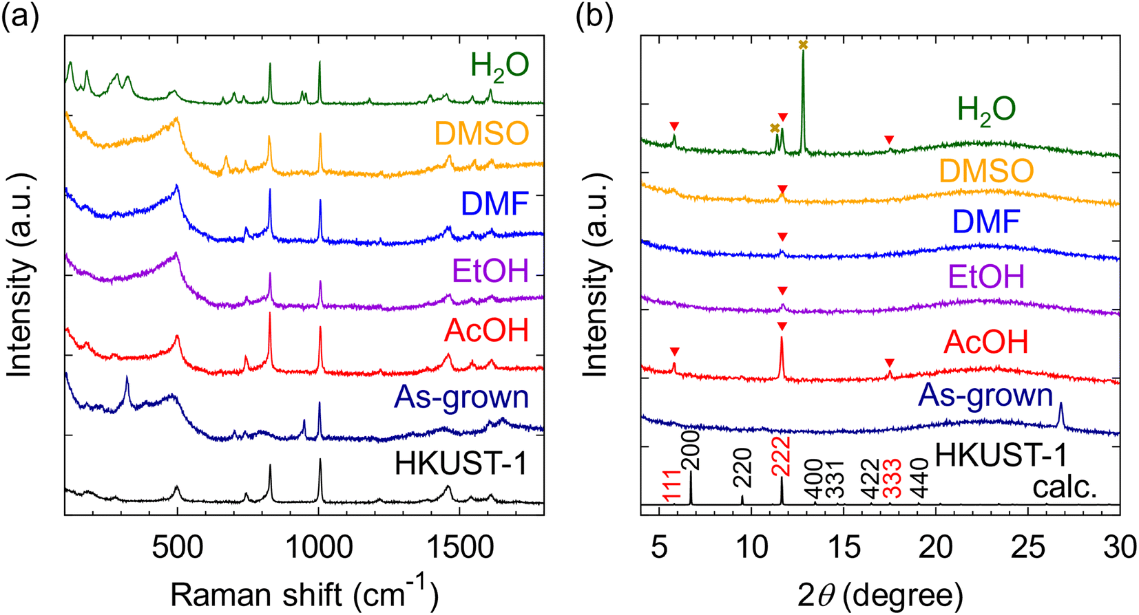 | ||
| Fig. 3 (a) Raman spectra and (b) out-of-plane X-ray diffraction patterns of thin films annealed with different solvent vapors: water (H2O), dimethyl sulfoxide (DMSO), N,N-dimethylformamide (DMF), ethanol (EtOH), and acetic acid (AcOH). Red triangles correspond to the 111, 220, 222, and 333 diffractions of HKUST-1, and yellow crosses indicate the unreacted precursors (Cu(OAc)2 and H3BTC). | ||
We further investigate the crystallinity of the thin films by XRD (Fig. 3b). In the case of annealing with H2O, the out-of-plane pattern shows the 111, 220, 222, and 333 diffractions (red triangles) of HKUST-1, indicating the formation of a polycrystalline HKUST-1 thin film. The peaks at 2θ = 11.3° and 12.8° (yellow crosses) correspond to the unreacted precursors, Cu(OAc)2 and H3BTC, respectively, consistent with the Raman spectrum (Fig. 3a). In the case of annealing with DMSO, DMF, or EtOH, only a weak 222 diffraction is observed, indicating the formation of low-crystallinity HKUST-1. The two-dimensional XRD patterns of the films annealed with DMSO, DMF, or EtOH vapor show a ring-shaped 222 diffraction, indicating the formation of polycrystalline HKUST-1 (Fig. S6†). Therefore, an oriented HKUST-1 film is not obtained by solvent vapor annealing with H2O, DMSO, DMF, or EtOH.
Notably, annealing with AcOH vapor successfully produces a (111)-oriented HKUST-1 thin film directly grown on a glass substrate (Fig. 3b). The intensities of the diffraction peaks of this film are higher than those of the other films, indicating superior crystallization. The 111, 222, and 333 diffractions of HKUST-1 are observed at 2θ = 5.8°, 11.7°, and 17.5°, respectively, indicating a (111) orientation. The two-dimensional XRD pattern shows a strong spot-like 222 diffraction and weak ring-shaped 222 diffraction, indicating a dominant (111)-oriented component and small polycrystalline components (Fig. S6†). HKUST-1 has two types of pores with different sizes, and the control of the crystal plane can selectively utilize one of these pores. Thus, a (111)-oriented HKUST-1 thin film has potential applications to highly selective gas sensors compared to polycrystalline ones.38 In addition, the in-plane XRD pattern indicates that the in-plane orientation is random (Fig. S7†). Deposition on a single crystalline substrate may provide an epitaxial thin film of HKUST-1 that has an out-of-plane and in-plane orientation.
Because AcOH vapor annealing is critical to obtaining a (111)-oriented HKUST-1 film, the effects of solvent volume on crystallinity and orientation are investigated by Raman spectroscopy and out-of-plane XRD (Fig. S8†). When annealed with 5 and 10 μL AcOH, the films only exhibit peaks consistent with those of HKUST-1 powder in their Raman spectra. In contrast, when annealed with 100 μL AcOH, the Raman peaks attributed to HKUST-1 are not observed, and H3BTC, Cu(OAc)2, and impurity peaks are observed. The impurity peaks include the ν(OH) of the partially coordinated H3BTC ligand39,40 at ∼1300 cm−1 and ν(CO) at ∼1650 cm−1. In the synthesis of HKUST-1 powder by the solvothermal method, excessive addition of AcOH results in the formation of other coordination compounds.20 The Raman spectra suggest that this is also the case for the synthesis of HKUST-1 films by solvent vapor annealing. When annealed with 10 and 100 μL AcOH, the films exhibit an impurity peak at 2θ = 8.9° in their out-of-plane X-ray diffraction patterns, which cannot be attributed to the precursors or HKUST-1 (Fig. S8b†). Therefore, excessive AcOH addition leads to the incomplete reaction of H3BTC and Cu(OAc)2, leaving unreacted precursors and another coordination compound.
We also investigate the effect of the stoichiometric ratio of Cu(OAc)2 and H3BTC on the growth of HKUST-1 (Fig. S9 and S10†). When metal or ligand precursor is in excess, Raman spectra and optical microscope images indicate that the excess precursor is aggregated, revealing that it is vital to control the stoichiometric ratio (film thickness) of the precursor films.
Furthermore, we test the influence of the deposition sequence of the precursors. Fig. S11† shows the out-of-plane XRD patterns of the thin films synthesized in different deposition sequences. As shown above, when H3BTC is first deposited, (111)-oriented HKUST-1 forms. In contrast, when Cu(OAc)2 is first deposited, polycrystalline HKUST-1 forms. Therefore, depositing the H3BTC layer first is important for the synthesis of (111)-oriented HKUST-1 films.
The depth profiles obtained by SIMS confirm that AcOH vapor annealing sufficiently promotes the diffusion of Cu(OAc)2 and H3BTC (Fig. 4a). The increase in the Si− intensity at a sputtering time of 100 s corresponds to the formation of an interface between the HKUST-1 film and glass substrate. The ambiguous interface compared to that in the as-grown film (Fig. S3†) is attributed to the large surface roughness caused by AcOH vapor annealing. The root-mean-square roughness measured by AFM is 29 nm, whereas that of the as-grown film is 2 nm (Fig. S12†). The large surface roughness is attributed to the large, sparsely crystallized HKUST-1 particles on the surface (Fig. 4b), as will be discussed later. More moderate annealing conditions can decrease surface roughness; hence, the conditions will be optimized in future work. The SIMS profiles of the (111)-oriented HKUST-1 film obtained by AcOH vapor annealing (Fig. 4a) show a relatively uniform distribution of H−, C−, O−, and Cu− compared to those in the as-grown and annealed-in-air films (Fig. 2b and S3†). This result indicates that AcOH vapor annealing enables the sufficient diffusion of the precursors. The film thickness measured using a stylus surface profiler is ∼300 nm (Fig. S13†). The calculated thickness of HKUST-1 formed using 100 nm of the Cu(OAc)2 layer is 330 nm, consistent with the measured thickness. Therefore, PVD combined with AcOH vapor annealing produces a film approximately six times thicker than that obtained by MOF-CVD (∼54 nm).15 This is because the gas–solid reaction in MOF-CVD limits the ability to produce a thicker film in principle. In addition, we can increase the thickness of (111)-oriented HKUST-1 thin films to ∼450 nm by increasing deposition cycles. Increasing the number of cycles reduces orientation (Fig. S14†) and surface flatness, probably due to the aggregation of HKUST-1 particles, which will be improved by optimization of annealing conditions.
 | ||
| Fig. 4 (a) Depth profiles obtained by secondary ion mass spectroscopy and (b) scanning electron microscopy image of the (111)-oriented HKUST-1 thin film. (c) Proposed mechanism for the (111)-oriented growth of HKUST-1. | ||
SEM analyzes the surface morphology of the (111)-oriented HKUST-1 film (Fig. 4b and S15†). The SEM image shows hexagonal facets, which can be interpreted as the (111) plane of the cubic structure. EDS mapping and point analysis confirm that Cu is distributed throughout the surface, with a large amount located in the hexagonal facets (Fig. S16 and S17†). The Raman spectrum and XRD pattern of the film annealed with AcOH vapor (Fig. 3) indicate that the film does not contain Cu(OAc)2 and is primarily composed of (111)-oriented HKUST-1 particles. Thus, the Cu widely distributed on the surface is not derived from Cu(OAc)2 but from small, aggregated (111)-oriented HKUST-1 particles. Furthermore, the AFM images also show the morphology of (111)-oriented HKUST-1 thin film (Fig. S12†). In the topographic image in Fig. S12a,† the film thickness is not uniform as in the SEM images and EDS mappings. In contrast, the phase image in Fig. S12b† is uniform throughout the film, indicating that HKUST-1 covers the entire substrate surface.
As discussed above, although solvent vapor annealing with EtOH, DMF, or DMSO forms HKUST-1, probably owing to the enhanced diffusion and reaction of the precursors (Fig. 3), the crystallinity is low, and polycrystalline HKUST-1 films are obtained. (111)-Oriented HKUST-1 is obtained only when the film is annealed with AcOH vapor, which is the key to control orientation. The SEM image suggests that AcOH has an influence on the stabilization of the (111) plane (Fig. 4b). The observed hexagonal particles correspond to the (111) plane of octahedral or truncated octahedral particles along the out-of-plane direction, and these particles are aggregated on the surface. In the solvothermal synthesis of HKUST-1 powder, octahedral or faceted octahedral HKUST-1 particles were obtained by adding monocarboxylic acid as the coordination modulator.29,41 These researches indicate that AcOH stabilized the (111) plane by controlling the coordination equilibrium between the metal ion and ligand. Furthermore, a previous theoretical study reported that coordinating AcOH to the HKUST-1 surface changes the surface energy.42 This study assumed that AcOH is coordinated to the Cu sites on the HKUST-1 surface, and surface energy calculations indicate that the (111) surface is the most stable. Therefore, AcOH vapor annealing can stabilize the (111) plane of HKUST-1 through the adsorption of AcOH on the surface, leading to the spontaneous orientation of the (111) plane on the glass substrate (Fig. 4c). In contrast, since the glass substrate is amorphous, it has little effect on the oriented growth of HKUST-1.
The use of other monocarboxylic acids, such as formic and propionic acid, in solvent vapor annealing, is also investigated (Fig. S18†). When annealed with propionic acid, the film exhibits Raman peaks consistent with those of HKUST-1 powder, and its out-of-plane XRD pattern shows only a weak 222 diffraction, indicating the formation of low-crystallinity HKUST-1. When annealed with formic acid, the film exhibits Raman peaks identical to those of H3BTC, and its out-of-plane XRD pattern shows a diffraction peak at 2θ = 17.2°, corresponding to the 420 reflection of H3BTC. Therefore, similar to the case of bulk synthesis, the acidity and side chain length of the carboxylic acid appear to affect the products and crystallinity significantly. Although other carboxylic acids may enhance the orientation when the amount added and temperature are optimized, in this study, AcOH vapor annealing is the best way to obtain a (111)-oriented HKUST-1 thin film.
Furthermore, we investigate the applicability of PVD combined with solvent vapor annealing to various MOFs. We synthesize thin films of well-known three-dimensional MOFs, UiO-66 and UiO-66-(OH)2, on a glass substrate. The XRD patterns show the formation of polycrystalline UiO-66 and UiO-66-(OH)2 (Fig. 5). The thickness of both films is ∼150 nm and the root mean square roughness is ∼40 nm (Fig. S19†). The synthesis of oriented thin films can be achieved by optimizing the precursor ratio and/or annealing conditions, which is a subject of future work.
 | ||
| Fig. 5 Out-of-plane X-ray diffraction patterns of (a) UiO-66 and (b) UiO-66-(OH)2 thin films on a glass substrate. | ||
In addition to two-dimensional conductive MOFs,17 HKUST-1, UiO-66, and UiO-66-(OH)2 films with an isotropic three-dimensional framework can be directly grown on an insulating substrate by PVD combined with solvent vapor annealing. The proposed method can be applied to various MOFs by tuning the solvent vapor annealing conditions using knowledge of bulk MOF synthesis and liquid-phase thin-film synthesis. It can minimize the amount of solvent used and avoid interface contamination due to immersion in the liquid solvent, which occurs in MOF-CVD and liquid-phase methods that utilize surface modification.12,15 Understanding interfacial phenomena between MOFs and functional materials is paramount in MOF applications. For instance, in composite materials combining HKUST-1 and metal nanoparticles, charge transfer at the interface significantly changes material properties.43 Additionally, at the interface of the band insulator Cu(II)-BPyDC (BPyDC = 2,2′-bipyridene-4,4′-dicarboxylate) and Mott insulator Cu(I)-TCNQ (TCNQ = 7,7,8,8-tetracyanoquinodimethane), metal conduction occurs through charge transfer.44 Because the proposed method enables the direct growth of MOFs on substrates with a uniform interface without contamination, this study paves the way for a detailed investigation of the structure, composition, and electronic states of interfaces.
In summary, we successfully achieved the synthesis of a (111)-oriented HKUST-1 film directly on an insulating glass substrate by PVD and AcOH vapor annealing. We demonstrate that AcOH is crucial for oriented growth. The proposed method can also be applied to the thin-film synthesis of other isotropic three-dimensional MOFs, UiO-66 and UiO-66-(OH)2. This research will advance the device applications and interface studies of various MOFs, including HKUST-1, UiO-66, and its analogs.
Author contributions
S. I.: formal analysis, investigation (lead), and writing of the original draft; R. N.: conceptualization (lead), investigation (supporting), draft editing (lead), supervision (lead), and funding acquisition; S. C.: draft editing (supporting) and investigation (supporting); R. S.: draft editing (supporting) and supervision (supporting); T. H.: draft editing (supporting), supervision (supporting), and funding acquisition. All authors have given approval to the final version of the manuscript.Conflicts of interest
The authors declare that they have no known competing financial interests.Acknowledgements
This work was supported by the Japan Society for the Promotion of Science (JSPS) Kakenhi (Grant No. 22K14692) and the Japan Science and Technology Agency (JST) Core Research for Evolutional Science and Technology (CREST) (Grant No. JPMJCR20T3 and JPMJCR22O4). The authors thank Dr Akira Genseki of the Materials Analysis Division, Open Facility Center, Tokyo Institute of Technology, for assistance with the SIMS measurements. Raman measurements were performed using research equipment shared in the Ministry of Education, Culture, Sports, Science and Technology (MEXT) Project for promoting public utilization of advanced research infrastructure (Program for supporting the introduction of the new sharing system) (Grant No. JPMXS0420900521). We thank Dr Yoshihisa Sei and Mr Kei Takihara for their assistance with the AFM measurements. We also acknowledge Editage (https://www.editage.jp/) for English language editing. The VESTA45 software was used to illustrate the crystal structure and simulate the XRD pattern of HKUST-1, UiO-66, and UiO-66-(OH)2.References
- H. Furukawa, K. E. Cordova, M. O'Keeffe and O. M. Yaghi, Science, 2013, 341, 1230444 CrossRef PubMed.
- J.-R. Li, R. J. Kuppler and H.-C. Zhou, Chem. Soc. Rev., 2009, 38, 1477–1504 RSC.
- J. Lee, O. K. Farha, J. Roberts, K. A. Scheidt, S. T. Nguyen and J. T. Hupp, Chem. Soc. Rev., 2009, 38, 1450–1459 RSC.
- M. Sadakiyo and H. Kitagawa, Dalton Trans., 2021, 50, 5385–5397 RSC.
- I. Stassen, N. Burtch, A. Talin, P. Falcaro, M. Allendorf and R. Ameloot, Chem. Soc. Rev., 2017, 46, 3185–3241 RSC.
- L. E. Kreno, K. Leong, O. K. Farha, M. Allendorf, R. P. Van Duyne and J. T. Hupp, Chem. Rev., 2012, 112, 1105–1125 CrossRef CAS PubMed.
- Q.-L. Zhu and Q. Xu, Chem. Soc. Rev., 2014, 43, 5468–5512 RSC.
- S. S.-Y. Chui, S. M.-F. Lo, J. P. H. Charmant, A. G. Orpen and I. D. Williams, Science, 1999, 283, 1148–1150 CrossRef CAS PubMed.
- A. A. Talin, A. Centrone, A. C. Ford, M. E. Foster, V. Stavila, P. Haney, R. A. Kinney, V. Szalai, F. El Gabaly, H. P. Yoon, F. Léonard and M. D. Allendorf, Science, 2014, 343, 66–69 CrossRef CAS PubMed.
- N. C. Jeong, B. Samanta, C. Y. Lee, O. K. Farha and J. T. Hupp, J. Am. Chem. Soc., 2012, 134, 51–54 CrossRef CAS PubMed.
- L. Shen, H. B. Wu, F. Liu, J. L. Brosmer, G. Shen, X. Wang, J. I. Zink, Q. Xiao, M. Cai, G. Wang, Y. Lu and B. Dunn, Adv. Mater., 2018, 30, 1707476 CrossRef PubMed.
- E. Biemmi, C. Scherb and T. Bein, J. Am. Chem. Soc., 2007, 129, 8054–8055 CrossRef CAS PubMed.
- O. Shekhah, H. Wang, S. Kowarik, F. Schreiber, M. Paulus, M. Tolan, C. Sternemann, F. Evers, D. Zacher, R. A. Fischer and C. Wöll, J. Am. Chem. Soc., 2007, 129, 15118–15119 CrossRef CAS PubMed.
- J.-L. Zhuang, D. Ceglarek, S. Pethuraj and A. Terfort, Adv. Funct. Mater., 2011, 21, 1442–1447 CrossRef CAS.
- J. Gascon, S. Aguado and F. Kapteijn, Microporous Mesoporous Mater., 2008, 113, 132–138 CrossRef CAS.
- V. V. Guerrero, Y. Yoo, M. C. McCarthy and H.-K. Jeong, J. Mater. Chem., 2010, 20, 3938–3943 RSC.
- J.-C. Lee, J.-O. Kim, H.-J. Lee, B. Shin and S. Park, Chem. Mater., 2019, 31, 7377–7385 CrossRef CAS.
- P. Su, M. Tu, R. Ameloot and W. Li, Acc. Chem. Res., 2022, 55, 186–196 CrossRef CAS PubMed.
- S. Han and C. B. Mullins, ChemSusChem, 2020, 13, 5433–5442 CrossRef CAS PubMed.
- D. Zacher, A. Baunemann, S. Hermes and R. A. Fischer, J. Mater. Chem., 2007, 17, 2785 RSC.
- S. Rodríguez-Hermida, D. E. Kravchenko, N. Wauteraerts and R. Ameloot, Inorg. Chem., 2022, 61, 17927–17931 CrossRef PubMed.
- S. Han, R. A. Ciufo, M. L. Meyerson, B. K. Keitz and C. B. Mullins, J. Mater. Chem. A, 2019, 7, 19396–19406 RSC.
- I. Stassen, M. Styles, G. Grenci, H. V. Gorp, W. Vanderlinden, S. D. Feyter, P. Falcaro, D. D. Vos, P. Vereecken and R. Ameloot, Nat. Mater., 2016, 15, 304–310 CrossRef CAS PubMed.
- S. Chon, R. Nakayama, S. Iwamoto, S. Kobayashi, R. Shimizu and T. Hitosugi, ACS Appl. Mater. Interfaces, 2023, 15, 56057–56063 CrossRef CAS PubMed.
- C. Scherb, A. Schödel and T. Bein, Angew. Chem., Int. Ed., 2008, 47, 5777–5779 CrossRef CAS PubMed.
- M. Schlesinger, S. Schulze, M. Hietschold and M. Mehring, Microporous Mesoporous Mater., 2010, 132, 121–127 CrossRef CAS.
- J. H. Cavka, S. Jakobsen, U. Olsbye, N. Guillou, C. Lamberti, S. Bordiga and K. P. Lillerud, J. Am. Chem. Soc., 2008, 130, 13850–13851 CrossRef PubMed.
- S. Yaginuma, J. Yamaguchi, M. Haemori, K. Itaka, Y. Matsumoto, M. Kondo and H. Koinuma, J. Phys.: Conf. Ser., 2007, 59, 520 CrossRef CAS.
- S. Maruyama, I. B. H. Prastiawan, K. Toyabe, Y. Higuchi, T. Koganezawa, M. Kubo and Y. Matsumoto, ACS Nano, 2018, 12, 10509–10517 CrossRef CAS PubMed.
- H. Oguchi, S. Kim, S. Maruyama, Y. Horisawa, S. Takagi, T. Sato, R. Shimizu, Y. Matsumoto, T. Hitosugi and S. Orimo, ACS Appl. Electron. Mater., 2019, 1, 1792–1796 CrossRef CAS.
- R. Nakayama, Y. Kawaguchi, R. Shimizu, K. Nishio, H. Oguchi, S. Kim, S. Orimo and T. Hitosugi, Cryst. Growth Des., 2022, 22, 6616–6621 CrossRef CAS.
- T. Miyadera, T. Sugita, H. Tampo, K. Matsubara and M. Chikamatsu, ACS Appl. Mater. Interfaces, 2016, 8, 26013–26018 CrossRef CAS PubMed.
- S. Głowniak, B. Szczęśniak, J. Choma and M. Jaroniec, Mater. Today, 2021, 46, 109–124 CrossRef.
- K. B. Lausund and O. Nilsen, Nat. Commun., 2016, 7, 13578 CrossRef CAS PubMed.
- A. Umemura, S. Diring, S. Furukawa, H. Uehara, T. Tsuruoka and S. Kitagawa, J. Am. Chem. Soc., 2011, 133, 15506–15513 CrossRef CAS PubMed.
- R. A. McDonald, S. A. Shrader and D. R. Stull, J. Chem. Eng. Data, 1959, 4, 311–313 CrossRef CAS.
- C. Prestipino, L. Regli, J. G. Vitillo, F. Bonino, A. Damin, C. Lamberti, A. Zecchina, P. L. Solari, K. O. Kongshaug and S. Bordiga, Chem. Mater., 2006, 18, 1337–1346 CrossRef CAS.
- Y. Wang, Y. Ban, Z. Hu and W. Yang, Nat. Commun., 2023, 14, 6617 CrossRef CAS PubMed.
- J. B. DeCoste, G. W. Peterson, H. Jasuja, T. G. Glover, Y. Huang and K. S. Walton, J. Mater. Chem. A, 2013, 1, 5642–5650 RSC.
- N. Nijem, K. Fürsich, S. T. Kelly, C. Swain, S. R. Leone and M. K. Gilles, Cryst. Growth Des., 2015, 15, 2948–2957 CrossRef CAS.
- S. Diring, S. Furukawa, Y. Takashima, T. Tsuruoka and S. Kitagawa, Chem. Mater., 2010, 22, 4531–4538 CrossRef CAS.
- S. Amirjalayer, M. Tafipolsky and R. Schmid, J. Phys. Chem. Lett., 2014, 5, 3206–3210 CrossRef CAS PubMed.
- Y. Chen, O. Sakata, Y. Nanba, L. S. R. Kumara, A. Yang, C. Song, M. Koyama, G. Li, H. Kobayashi and H. Kitagawa, Commun. Chem., 2018, 1, 61 CrossRef.
- P. Sindhu, K. S. Ananthram, A. Jain, K. Tarafder and N. Ballav, Nat. Commun., 2022, 13, 7665 CrossRef CAS PubMed.
- K. Momma and F. Izumi, J. Appl. Crystallogr., 2011, 44, 1272–1276 CrossRef CAS.
Footnote |
| † Electronic supplementary information (ESI) available. See DOI: https://doi.org/10.1039/d4ta01298d |
| This journal is © The Royal Society of Chemistry 2024 |