 Open Access Article
Creative Commons Attribution 3.0 Unported Licence
Unravelling the chloride dopant induced film improvement in all-inorganic perovskite absorbers†
Stefan
Nicholson
 ab,
Jochen
Bruckbauer
 b,
Paul R.
Edwards
 b,
Carol
Trager-Cowan
 b,
Robert W.
Martin
 b and
Aruna
Ivaturi
 *a
*a
aSmart Materials Research and Device Technology Group, Department of Pure and Applied Chemistry, University of Strathclyde, Glasgow G1 1XL, UK. E-mail: aruna.ivaturi@strath.ac.uk
bSemiconductor Spectroscopy and Devices Group, Department of Physics, SUPA, University of Strathclyde, Glasgow G4 0NG, UK
First published on 16th July 2024
Abstract
CsPbI2Br perovskite material has been the focus of much recent research, thanks to its improved stability over CsPbI3, useful bandgap of 1.9 eV and enhanced thermal stability over hybrid perovskite materials with volatile organic components. It has great potential for both single junction solar cells for indoor applications, and implementation in tandem cells. However, moisture stability has remained an issue. In order to overcome this roadblock towards commercialisation, metal chloride dopants have been widely investigated to improve film quality and reduce damage from humidity. Most of the studies report that the metal cation in the dopant plays a greater role in the improvement of the film properties than the chloride anions, which are thought to be removed during annealing in some studies. The majority of the research to date on this topic has focussed on investigating device performance and bulk film characteristics, with limited attention paid to grain-level crystallinity and whether the dopant is proportionally incorporated into the film. In the present work, cathodoluminescence (CL) and electron backscatter diffraction (EBSD) are utilised to investigate the effects of a lead chloride dopant, both on emission and crystal structure at a grain level, with the findings supported by X-ray diffraction (XRD). Confirmation of proportional incorporation of the dopant into the final prepared films is provided by wavelength dispersive X-ray (WDX) spectroscopy. This work provides valuable insight into the impact chloride dopants have on all-inorganic perovskite absorbers, helping to influence future dopant strategies.
Introduction
Within the currently looming global energy crisis, our future energy needs will be delivered by a range of green energy sources including wind, hydro-electric and solar power. Globally, solar energy generation already surpassed 1000 TW h in 2021,1 and this is expected to grow rapidly as we move further towards carbon-free green energy. With solar power expected to form a significant portion of future energy, solar cell research has grown, particularly in the field of metal halide perovskite absorbers.2 These materials exhibit an ABX3 structure, with the A site typically formed of an organic or inorganic cation, the B site normally being lead or some other metal cation, and the X site consisting of halide anions. In the published work to date, a wide range of perovskites have been explored, in particular hybrid perovskites with organic methylammonium (MA) or formamidinium (FA) groups.3–7 Currently FAPbI3 leads the way in efficiency with a state-of-the-art power conversion efficiency of 25.7%.8 However, thermal stability concerns due to the volatile organic groups, and relatively poor air stability mean that it is desirable to explore other perovskite materials.9–12 One of the most promising approaches to address the stability issues of organic cations is to replace them with inorganic cations, such as caesium, for developing all-inorganic perovskite (e.g. CsPbI2Br) solar cells. The inorganic CsPbI2Br absorber has a large bandgap of around 1.9 eV, and increased thermal and light stability.13,14 This bandgap makes the material useful for both outdoor (as the top cell in tandem solar cells) and indoor light capture.15,16 Thanks to these properties, and an estimated efficiency of 31% when used in a tandem Si-perovskite solar cell,17 the material has attracted extensive research interest. There are however some drawbacks to the use of this all-inorganic material: poor moisture stability13,18 and high defect density.19,20 These issues can be overcome by the addition of dopants to the perovskite film, to passivate defects,21,22 or incorporation of the dopant into the lattice to change the tolerance factor,23 as demonstrated via europium doping.24 Dopants can also be added to the electron transport layer to have a passivating effect through this interface of the cell impacting on the layers, as demonstrated widely in the literature, particularly in dual passivation methods.25–27 A range of dopants or treatments are reported in the literature, with a large variety of elements covered.18,21,24,28–36 A large number of these dopants are metal salts containing chloride as their anion, and this has become a popular choice. A selection of these have been shown in Table 1, with their attributed purpose summarised. Some of these dopants are stated to have several roles in improving the device performance. However, in many cases the specific method of action of the dopant cannot be conclusively determined, despite the dopant being a component of the precursor solution. As shown within the table, there are a number of papers quoting device improvements following the introduction of dopants containing a chloride anion. Several of these papers quote grain size enlargement or improved morphology as part of the action of the dopant,19,31,35,38,43 however this cannot to date be visualised or linked to the crystallography on a grain level. X-ray diffraction (XRD) in these cases provides bulk film characteristics; however detailed structural information on the grain level is not obtained by adopting this bulk approach. A more suitable approach for investigating the impact of a dopant on the film's crystallinity is that of electron backscatter diffraction (EBSD), shown previously to give in-depth information about the crystal orientation and misorientation within films and grains.44–46 Where chloride has been studied, the effects on emission are dismissed as limited, despite photoluminescence emission shown to be improved by the addition of PbCl2.47 Shifts in the PL emission peaks in the study involving InCl3 dopants have been suggested to be from the hot air treatment during film formation rather than due to the dopant.35 Also, most of the studies report that the metal cation in the dopant plays a greater role in the improvement of the film properties of CsPbI2Br films than the chloride anions.19,31,34,35,37–42 Attempts to probe chloride incorporation into the CsPbI2Br films has been shown with varying amounts of success, with some report it to be removed during annealing.33 Some of the techniques commonly explored for such attempts are listed in Table 1.| Dopant(s) used | Effect of the dopant | Technique used to investigate chloride presence | Reference |
|---|---|---|---|
| CsCl | Larger grain growth and compact film created, with reduced defects and increased carrier lifetime | Chloride presence was not evident from XPS studies | 19 |
| MnCl2 | Reduced defect density with improved polycrystalline film formation. Reduced trap states | EDX maps revealed that all of the elements, including Mn and Cl, were distributed homogeneously throughout the film | 31 |
| CaCl2 | Reduced trap density and change of Fermi levels of perovskite with CaCl2. No changes observed using PbCl2 | XPS measurements carried out to probe chloride dopant. Very low intense Cl 2p signal | 34 |
| PbCl2 | |||
| InCl2 | Improved morphology, crystal orientation and reduced defects, leading to increased carrier lifetime | Cl− presence not probed | 35 |
| EuI3 | |||
| SrCl2 | Improved morphology. Reduced hysteresis. Increased carrier lifetimes. Removal of trap states | Cl− presence not probed | 37 |
| NiCl2 | |||
| PbCl2 | Trap state density reduced with improved emission | XPS measurements carried out to probe chloride dopant | 38 |
| Better crystallisation through improved coverage and crystal orientation, and larger grain sizes | |||
| NbCl5 | Reduces charge recombination. Negligible hysteresis | Cl− presence not probed in XPS | 39 |
| GdCl3 | Dense perovskite film with small grains, suppressed charge carrier recombination, appropriate energy level alignment. No changes observed using PbCl2 | Cl− shown in EDX maps. Authors claim Gd effect, Cl passivates at grain boundaries | 40 |
| PbCl2 | |||
| FeCl2 | Grain size reduction, align the energy levels, promote the built-in potential (Vbi), and reduce the defect states in the perovskite | Cl− appears in EDX maps. XPS not shown | 41 |
| MACl | The MACl dopant effectively increases the crystallinity and grain size of CsPbI2Br film by retarding the crystallization rate of perovskite | TOF-SIMS shows presence of Cl− at very bottom of film, at interface with TCO | 42 |
In contrast, in hybrid organic–inorganic halide perovskites Cl incorporation is demonstrated to be beneficial for defect passivation mainly at the heterojunction interfaces, but is often reported to be undetectable.48–50 In some studies the concentration of Cl in hybrid organic–inorganic halide perovskite films is varied by changing the duration of annealing due to the volatile nature of perovskite components. The chloride content in the films was analysed using WDX analysis.51
In the present study, electron backscatter diffraction (EBSD) and X-ray diffraction (XRD), along with cathodoluminescence (CL) and wavelength dispersive X-ray spectroscopy (WDX) studies have been explored to unravel the influence of chloride anions and their role in improving film properties of all-inorganic CsPbI2Br perovskite absorbers doped using PbCl2. Detailed grain level structural and optoelectronic properties as a function of dopant concentration confirmed proportional incorporation of chloride ions into the films, and revealed their important role in dictating the crystal orientation and emission at the grain level.
Experimental
Materials
Lead iodide (99.99% trace metals basis) and lead bromide (99.98% trace metals basis) were purchased from TCI Chemicals, dimethyl sulfoxide (99.8% + extra dry) from Acros Organics, caesium iodide (99.999% trace metals basis), lead(II) chloride (≥98%) and tin(IV) chloride pentahydrate (98%) from Sigma Aldrich, ethanol (≥99.8%, absolute, analytical reagent grade) from Fisher, acetone (≥99.5%) and 2-propanol (≥99.7%) from VWR International LLC. TEC 15 fluorine doped tin oxide (FTO)-coated glass were obtained from NSG Pilkington Ltd.Film preparation
FTO-coated glass substrates were cut (1.5 cm × 2 cm) and cleaned by scrubbing with a 2% Hellmanex™ solution. The substrates were then thoroughly rinsed with deionised water, before being placed in a substrate holder. They were then sonicated subsequently in deionised water, isopropanol, and acetone, for 15 minutes each. Following this, the substrates were blown dry with compressed air, and O2 plasma-cleaned for 15 minutes. The SnO2 precursor solution was prepared by mixing 0.225 g SnCl2·2H2O in 10 ml ethanol by stirring overnight. The solution was spin coated at 3000 rpm for 30 seconds on the FTO-coated glass substrates, and then annealed at 100 °C for 10 minutes, followed by 180 °C for 1 hour. Following deposition, the substrates were O2 plasma treated prior to immediate transfer to the N2 filled glovebox. The CsPbI2Br precursor was prepared by mixing 312 mg CsI, 277.7 mg PbI2 and 220 mg PbBr2 in 1 ml dimethyl sulfoxide (DMSO) as reported elsewhere.52 For doped samples, PbCl2 was added to the CsPbI2Br precursor to make either 1 mol% (1.7 mg ml−1), 3 mol% (5.0 mg ml−1) or 5 mol% (8.3 mg ml−1) PbCl2. The solutions were stirred at 60 °C for 1 hour and then aged overnight. The perovskite precursor was then spin coated on the substrates at 2000 rpm for 120 seconds, followed by annealing for 2 minutes at 50 °C and 10 minutes at 160 °C or 2 min at 280 °C. This step was precisely controlled to ensure no unintended compositional variation between the samples. For samples deposited for XRD only, a coating of PMMA (10 mg ml−1 in chlorobenzene) was applied by spin coating at 4000 rpm for 20 seconds. This was to act as a protective layer for the films exposed to air during XRD measurements. Other measurements were carried out under vacuum, and as such the PMMA coating was not necessary.Film characterisation and analysis
CL and EBSD measurements along with secondary electron imaging were performed using a FEI Quanta 250 FEG microscope.53 For room temperature CL measurements, an accelerating voltage of 4 kV and a 400 lines per mm 500 nm blaze grating was selected to capture the expected 650 nm emission peak. The CL measurements were carried out at a 45° tilt angle to direct the light into the lens of the bespoke CL system. Maps were taken across a 10 × 10 μm area, with a step size of 0.2 μm, with a 50 μm slit attached to the 1/8 m spectrograph. The EBSD measurements were performed using an Oxford Instruments Nordlys EBSD detector. EBSD maps of 60 × 50 pixel area were acquired at an accelerating voltage of 20 kV, a sample tilt of 70°, a step size of 100 nm and pattern resolution of 336 × 256 px2. The EBSD data was indexed using Oxford Instruments' Refined Accuracy method and analysed using the Matlab-based toolbox MTEX.54,55 The XRD measurements were performed at room temperature on a Bruker D2 Phaser system using monochromatic CuKα radiation with a wavelength of 1.5406 Å. The samples were scanned in the range 5–80° with an increment of 0.04° on the 2θ scale. The substrates were set to a rotation speed of 8 rpm throughout the measurement. WDX data was collected on a JEOL JXA-8530F electron microprobe using a TAP diffracting crystal to detect Cl− Kα X-rays excited by a beam energy of 10 keV with a current of 100 nA. To investigate migration of Cl− (if any) from SnO2 and FTO layers, WDX maps of the cross-section of an undoped perovskite film deposited on SnO2 electron transport layer covered FTO coated glass, was investigated. The cross-section sample was prepared from the same spin-coating method described above. To avoid charging as much as possible during WDX maps, the film was mounted with the perovskite film surface facing against metal, and carbon was sputtered on top. For cross-section WDX maps, the scans were taken on a JEOL JXA-8530F EPMA system at 10 kV, with 10 nA current, with a 75 ms dwell per pixel, across 100 × 75 pixels, with a 17 nm step size. For WDX scans the following crystals were used – TAPH for Br Lα; PETJ for Sn Lα; and PETH for Cl Kα.Results and discussion
The impact of the chloride dopant on the crystallographic structure of the perovskite thin film was investigated by XRD and EBSD. XRD pattern shows three main peaks, as seen in Fig. 1(A), at 15.2°, 21.5° and 30.2° corresponding to the (100), (110) and (200) crystallographic planes of α-CsPbI2Br, respectively.56 The lack of new peaks when comparing undoped CsPbI2Br to the one with highest dopant concentration shows that PbCl2 is not present as a separate species in the final film. The PbCl2 would result in the appearance of a dominant peak at approximately 22.8°.57 The intensity of the diffraction peaks increase with the addition of PbCl2, with the exception of the 5% concentration, with a maximum for 1% concentration. A closer view of the (200) peak as seen in Fig. 1(B), reveals a shift towards higher angles in the 2θ scan, indicating the contraction of the perovskite lattice as it incorporates the smaller chloride anions. The level of shift increases as higher concentrations of dopant are used, indicating a correlative effect.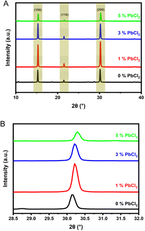 | ||
| Fig. 1 (A) XRD pattern for undoped and doped (1, 3 and 5% PbCl2) CsPbI2Br films (B) magnified view showing shift in the (200) peak position with increase in dopant concentration. | ||
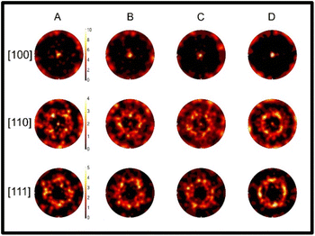
Inverse pole figure (IPF) maps obtained from the EBSD analysis are used to display the orientation of individual grains within the sample. IPF maps show the crystal directions with respect to the reference directions X, Y and Z, where X and Y are the two perpendicular in-plane directions and Z the out-of-plane direction corresponding to the sample normal. The IPF maps are shown in Fig. 2. From these plots one can note, that in all cases there is a random orientation of grains in the X–Y plane (i.e. in-plane). Within the IPF Z maps, one notices that the [100] and [110] orientations (red and green colours, respectively) are the dominant colours for the samples indicating the preferred orientation towards these directions. The map becomes more strongly [100] orientated in the highest dopant concentration case, confirming that the PbCl2 is strongly coordinating the film orientation at grain level. White regions on the IPF maps indicate regions where indexing was not possible due to low signal intensity from the sample, likely caused by the shadowing effect of large grains protruding from the sample surface or the lack of crystallinity in grain boundaries. The shadowing effect would be expected to be most prominent in the highest concentration case where the grains are larger. The IPF maps show [100] preferential orientation with increase in PbCl2 concentration across all of the samples with respect to the sample normal, indicated by the bright red colour which is dominant in the IPF Z maps as seen in Fig. 2, and the bright intense spot in the centre of the [100] pole figures as shown in Fig. 3. This correlates with the high intensity peaks from the XRD data.
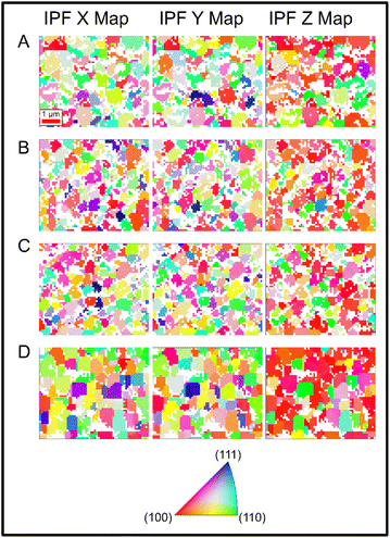 | ||
| Fig. 2 IPF maps showing grain level crystallographic orientation for PbCl2 doped CsPbI2Br films – (A) 0%, 0 mg ml−1, (B) 1%, 1.8 mg ml−1, (C) 3%, 5.0 mg ml−1, and (D) 5%, 8.4 mg ml−1. | ||
The [100] pole figure shows clear dominant orientation with respect to the sample normal, with all concentrations having a clear bright spot in the centre of the pole figure. This increases to a brighter spot nearly-off-scale for the highest dopant concentration, revealing the clear link between the dopant and orientation. From the [110] pole figures, it can be noted that there is a bright spot in the centre for all samples. This spot becomes less intense on addition of the dopant, indicating that the PbCl2 influences the film orientation. This implies a level of preferred orientation in the [110] direction, corresponding to the green grains in the IPF Z maps in Fig. 2, something which is undesirable for good CsPbI2Br film quality due to its metastable nature.58
The pole figures give an overview of how the entire film is crystallised, but do not reveal localised grain information and grain sizes. Band contrast maps generated from the EBSD measurement, which are a measure of quality of the EBSD patterns, can be used to give a visual indication of grain size across the samples, with areas in grain boundaries giving low intensity of diffraction patterns.59,60Fig. 4 contains the band contrast maps for the sample set, revealing an overall trend of increasing grain size for the sample with the highest dopant concentration.
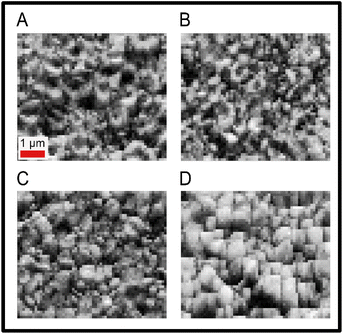 | ||
| Fig. 4 Band contrast maps for the sample set, pattern signal on intensity scale. PbCl2 doped CsPbI2Br (A) 0%, 0 mg ml−1, (B) 1%, 1.8 mg ml−1, (C) 3%, 5.0 mg ml−1, and (D) 5%, 8.4 mg ml−1. | ||
It is important to note that XRD gives crystallographic information from the overall thin film thickness whereas EBSD gives information from around ∼50 nm of the film from the surface. Comparing XRD and EBSD results, it can be noted that the sample with 1% of PbCl2 dopant concentration has the most intense XRD peaks which decreases as the dopant concentration increases. On the other hand, EBSD revealed that the film with 5% PbCl2 has the largest number of grains oriented along the preferential [100] direction in the sample normal. This indicates that as the chloride dopant concentration increases, the crystallites orientation along the preferred [100] direction is tuned first from within the bulk of the sample. To investigate this further, SnO2 electron transport layer deposited on FTO has also been analyzed using WDX to check for the presence of chlorine. As shown in Fig. S1,† both the FTO and SnO2 coated FTO revealed the presence of small concentration of chlorine in the layers. This chlorine though does not migrate into the perovskite layer [as confirmed by absence of any chlorine signal from the WDX analysis of the top surface of the undoped CsPbI2Br film (Fig. 7) as well as cross-section WDX analysis of the undoped CsPbI2Br film deposited on SnO2 coated FTO (Fig. S2 and S3†)], might however influence initiation of preferred orientation of the grains at the perovskite/SnO2 interface in PbCl2 doped perovskite films. With the increase in the concentration of PbCl2 there will be excess Pb2+ as well which might lead to decrease in crystallinity of the sample. Thus, at higher PbCl2 content though the EBSD analysis shows highest number of grains from near the surface of the films oriented along the [100] direction in the sample normal, the XRD analysis shows a decrease in the intensity of the diffraction peaks of CsPbI2Br for PbCl2 concentration higher than 1%.
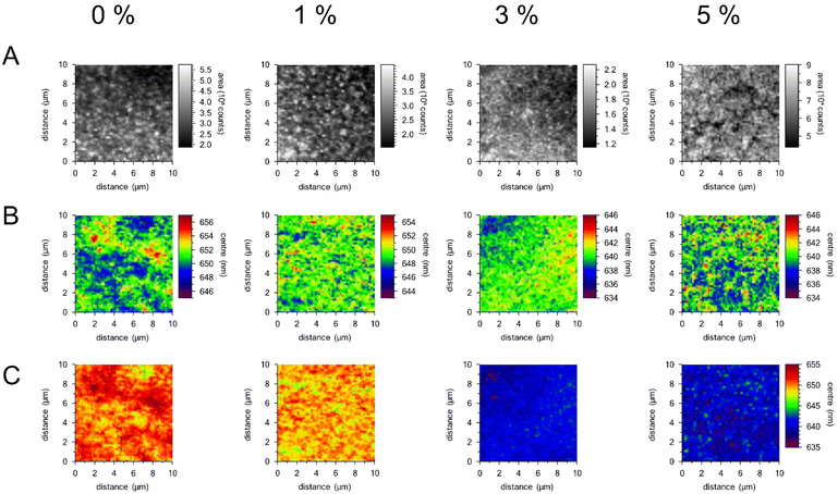
From the mean CL spectra shown in Fig. 5, one can note that the emission peak is blue shifted when the chloride concentration is increased, confirming the change to the band structure of the perovskite effected by the incorporation of the chloride ions. The shift between the peaks for the undoped and most highly doped sample, is approximately 10 nm or 0.03 eV. This is a significant change when considering the band alignment of a perovskite cell, and could lead to a marked change in efficiency, as reported in the literature.56,61,62 The incorporation of chloride ions to the perovskite lattice results in slight shifts in the LUMO and HOMO levels of the semiconductor material, which affects band alignment to the charge transport layers of the cell. Cell stacks need to be designed with this in mind. Within this study, concentrations of dopant have been kept low, showing dopant effects can be gained from a very low level. The peak shift and intensity can also be viewed across a scanned area of the sample surface by hyperspectral imaging. Within the integrated intensity maps displayed in Fig. 6(A), it is notable that there are large variations in intensity across the samples, with brighter emitting spots visible in the 0% and 1% samples before the highest concentration sample shows areas of weaker intensity at the grain boundaries of the larger grains in the sample. Shifts in wavelength of emission are displayed by plotting a map of the centre wavelength of a fitted peak at each pixel as a function of position, as shown in Fig. 6(B) and (C). Fig. 6(B) uses an identical wavelength range in each case, highlighting reduced inhomogeneity in the middle two samples, while the wavelength scale is kept the same for all plots in Fig. 6(C), to allow for direct comparisons between the samples to be made. Within these plots there is a general blueshift with increasing dopant concentration, however this is not uniform across the sample area.
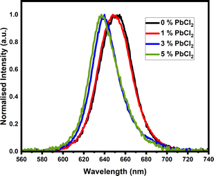 | ||
Fig. 5 Mean CL spectra (normalised), showing the average spectrum obtained using all 10![[thin space (1/6-em)]](https://www.rsc.org/images/entities/char_2009.gif) 000 pixels of the 10 × 10 μm scan. 000 pixels of the 10 × 10 μm scan. | ||
It is also notable that the intensity plots in Fig. 6 do not show a simple correlation with the shifts in wavelength, and the differences in wavelength across the samples appears to be a grain-based phenomenon, as opposed to simple variation between grain and grain boundary.51
So far, the effect on the crystallisation of the perovskite, and an effect on the cathodoluminescence has been shown. However, elemental composition data is helpful in conclusively attributing the effects observed to chloride incorporation in the films.
In this study WDX measurements were used in order to investigate the presence of chloride in the films. WDX analysis clearly confirms that the dopant is incorporated into the film and remains part of the structure, as opposed to playing a passive crystallisation modification role. Fig. 7 focusses solely on the Cl Ka peak measured using a PET (pentaerythritol) diffracting crystal. A clear and almost proportional appearance of the peak is observed as the dopant concentration increases, confirming the concentration dependant incorporation of Cl− into the perovskite.
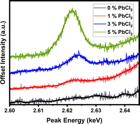 | ||
| Fig. 7 WDX peak for chlorine showing increasing concentration from increasing dopant content in precursor. | ||
With WDX confirming that the chlorine is present within the samples post-annealing, the lack of a PbCl2 peak in XRD, and shifts within the sole CL emission peak of the perovskite, it can be confidently inferred that chloride anions are incorporated into the perovskite lattice, with consequences on the band structure and grain sizes in the resulting material. In order to further probe the presence and retention of chloride anions into the lattice, the WDX experiment was further repeated on 5% doped sample annealed for different durations [pre-annealing for 2 minutes at 50 °C followed by 10, 30 and 60 minutes at 160 °C], to confirm whether extended annealing times would eventually result in the chloride volatilization from the CsPbI2Br film as reported for hybrid organic inorganic films. From Fig. 8, it can confirmed that the chloride remains within the lattice regardless of annealing length, and it is suggested that strong binding to the lattice and lack of volatile components in CsPbI2Br (in contrast to the organic–inorganic hybrid perovskites) prevent it from evaporating during the film crystallisation process.
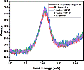 | ||
| Fig. 8 WDX peak for chlorine within a 5% PbCl2 doped sample, showing the effect of annealing time [pre-annealing for 2 minutes at 50 °C followed by 10, 30 and 60 minutes at 160 °C] on peak intensity. | ||
Finally, to confirm the impacts of the dopant on the stability of the films, films doped with various concentrations of PbCl2 were monitored under standard laboratory conditions. Fig. 9 shows the change in film appearance between freshly prepared samples, and after 90 minutes of exposure to the air and moisture. It can be clearly observed that an increase of PbCl2 content has an impact on the stability of the film, with films higher than 3% PbCl2 appearing less degraded.
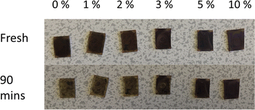 | ||
| Fig. 9 Picture of CsPbI2Br films doped with different concentrations of PbCl2, before and after exposure to ambient conditions for 90 minutes. | ||
Conclusions
In summary, a PbCl2 dopant is confirmed to result in chloride ion incorporation into CsPbI2Br perovskite films on a proportional, concentration dependant basis using WDX, XRD, EBSD and CL analysis. It has been demonstrated that the chloride is not evaporated during the annealing step of the film preparation, and that annealing duration does not impact on the chloride content. EBSD analysis confirms improved preferential orientation within the films with higher PbCl2 doping, confirming the dopant is manipulating and controlling the growth of the film. EBSD also indicates grain size increasing with the doping level, revealing that the nucleation process is slowed and allowing for greater grain growth. CL analysis shows that the incorporation of the chloride dopant proportionally impacts the emission wavelength of the films, suggesting that the bandgap is altered by chloride ion incorporation. XRD shows no evidence of PbCl2 incorporating as a separate phase, and peak shifts of the bulk perovskite show lattice contraction to incorporate the smaller chloride ions into the lattice. The incorporation of the chloride anion into the lattice enhances stability of the films, important towards the progression of a perovskite of this type. This work provides vital insights into the roles that chloride anionic dopants have in the formation of all-inorganic perovskite absorbers, key information towards the improvement of perovskite solar cells of this type.Data availability
All data underpinning this publication are openly available from the University of Strathclyde at https://doi.org/10.15129/33a44172-53aa-4911-81fd-6410876957fd.Author contributions
SN carried out and analysed most of the practical work and drafted the manuscript. JB carried out EBSD measurements and helped in data analysis with the support of CTC. PRE provided advice and training for CL and CL data analysis. AI conceptualised the work. AI and RWM supervised the work and helped in results interpretation. All the authors provided inputs to the manuscript.Conflicts of interest
The authors declare that they have no known competing financial interests that could appear to have influenced the work reported within this manuscript.Acknowledgements
AI would like to acknowledge the UK Research and Innovation (UKRI), Engineering and Physical Sciences Research Council (EPSRC) for the fellowship grant (EP/P011500/1). RWM acknowledges the EPSRC project “Nanoanalysis for Advanced Materials and Healthcare” (EP/N010914/1). CTC and JB would like to acknowledge the EPSRC for the grant (EP/P015719/1). JB would like to acknowledge the Royal Society of Edinburgh (RSE) for a Saltire International Collaboration Award (1917). The authors would like to acknowledge EPSRC DTP (2439071) and Strathclyde's Student Excellence Award (SEA) for funding SN's studentship.Notes and references
- International Energy Agency (IEA), Solar Photovoltaics Report, https://www.iea.org/energy-system/renewables/solar-pv, Accessed: date Search PubMed.
- Web of Science Search conducted 23/04/2024 ‘Perovskite AND Solar’.
- L. Duan, H. Zhang, M. Liu, M. Grätzel and J. Luo, ACS Energy Lett., 2022, 7, 2911–2918 CrossRef CAS.
- T. Niu, J. Lu, R. Munir, J. Li, D. Barrit, X. Zhang, H. Hu, Z. Yang, A. Amassian, K. Zhao and S. (Frank) Liu, Adv. Mater., 2018, 30, 1706576 CrossRef PubMed.
- V. Kojić, M. Bohač, A. Bafti, L. Pavić, K. Salamon, T. Čižmar, D. Gracin, K. Juraić, M. Leskovac, I. Capan and A. Gajović, Materials, 2021, 14, 4594 CrossRef PubMed.
- A. Valluvar Oli, Z. Li, Y. Chen and A. Ivaturi, ACS Appl. Energy Mater., 2022, 5, 14669–14679 CrossRef CAS PubMed.
- M. Balaji Gandhi, A. Valluvar Oli, S. Nicholson, M. Adelt, R. Martin, Y. Chen, M. Babu Sridharan and A. Ivaturi, Sol. Energy, 2023, 253, 1–8 CrossRef CAS.
- NREL, https://www.nrel.gov/pv/interactive-cell-efficiency.html, accessed 09/03/2023.
- Y. Rong, L. Liu, A. Mei, X. Li and H. Han, Adv. Energy Mater., 2015, 5, 1501066 CrossRef.
- T. Leijtens, G. E. Eperon, N. K. Noel, S. N. Habisreutinger, A. Petrozza and H. J. Snaith, Adv. Energy Mater., 2015, 5, 1500963 CrossRef.
- Y. A. Olanrewaju, K. Orisekeh, O. V. Oyelade, R. K. Koech, R. Ichwani, A. I. Ebunu, D. I. Amune, A. Bello, V. C. Anye, O. K. Oyewole and W. O. Soboyejo, AIP Adv., 2022, 12, 015122 CrossRef CAS.
- G. Abdelmageed, C. Mackeen, K. Hellier, L. Jewell, L. Seymour, M. Tingwald, F. Bridges, J. Z. Zhang and S. Carter, Sol. Energy Mater. Sol. Cells, 2018, 174, 566–571 CrossRef CAS.
- S. Mariotti, O. S. Hutter, L. J. Phillips, P. J. Yates, B. Kundu and K. Durose, ACS Appl. Mater. Interfaces, 2018, 10, 3750–3760 CrossRef CAS PubMed.
- Y. Long, K. Liu, Y. Zhang and W. Li, Molecules, 2021, 26, 3398 CrossRef CAS.
- Z. Guo, A. K. Jena, I. Takei, M. Ikegami, A. Ishii, Y. Numata, N. Shibayama and T. Miyasaka, Adv. Funct. Mater., 2021, 31, 2103614 CrossRef CAS.
- S. Choi, H. J. Lee, J. H. Heo and S. H. Im, EcoMat, 2022, 5, 1–10 Search PubMed.
- S. Xie, R. Xia, Z. Chen, J. Tian, L. Yan, M. Ren, Z. Li, G. Zhang, Q. Xue, H. L. Yip and Y. Cao, Nano Energy, 2020, 78, 105238 CrossRef CAS.
- Y. Li, Y. Wang, T. Zhang, S. Yoriya, P. Kumnorkaew, S. Chen, X. Guo and Y. Zhao, Chem. Commun., 2018, 54, 9809–9812 RSC.
- I. S. Jin, K. S. Kim and J. W. Jung, J. Power Sources, 2021, 512, 230481 CrossRef CAS.
- D. Han, S. Yi, Q. Yuan, X. Tang, Q. Shu, Q. Li, F. Wang, D. Y. Zhou and L. Feng, Small, 2021, 17, 1–10 Search PubMed.
- J. Lu, S. C. Chen and Q. Zheng, Sci. China Chem., 2019, 62, 1044–1050 CrossRef CAS.
- D. Han, Q. Yuan, Z. Slanina, X. Tang, S. Yi, D. Y. Zhou, F. Uhlik and L. Feng, Sol. RRL, 2021, 5, 1–9 Search PubMed.
- Z. Li, M. Yang, J.-S. Park, S.-H. Wei, J. J. Berry and K. Zhu, Chem. Mater., 2016, 28, 284–292 CrossRef CAS.
- W. Xiang, Z. Wang, D. J. Kubicki, W. Tress, J. Luo, D. Prochowicz, S. Akin, L. Emsley, J. Zhou, G. Dietler, M. Grätzel and A. Hagfeldt, Joule, 2019, 3, 205–214 CrossRef CAS.
- C. Liu, J. He, M. Wu, Y. Wu, P. Du, L. Fan, Q. Zhang, D. Wang and T. Zhang, Sol. RRL, 2020, 4, 2000016 CrossRef CAS.
- S. Liu, W. Chen, Y. Shen, S. Wang, M. Zhang, Y. Li and Y. Li, J. Mater. Chem. A, 2020, 8, 14555–14565 RSC.
- S. Zhang, H. Gu, S.-C. Chen and Q. Zheng, J. Mater. Chem. C, 2021, 9, 4240–4247 RSC.
- C. F. J. Lau, M. Zhang, X. Deng, J. Zheng, J. Bing, Q. Ma, J. Kim, L. Hu, M. A. Green, S. Huang and A. Ho-Baillie, ACS Energy Lett., 2017, 2, 2319–2325 CrossRef CAS.
- J. V. Patil, S. S. Mali and C. K. Hong, Sol. RRL, 2020, 4, 2000164 CrossRef CAS.
- W. Zhang, J. Xiong, J. Li and W. A. Daoud, Sol. RRL, 2020, 4, 2000112 CrossRef CAS.
- D. Bai, J. Zhang, Z. Jin, H. Bian, K. Wang, H. Wang, L. Liang, Q. Wang and S. F. Liu, ACS Energy Lett., 2018, 3, 970–978 CrossRef CAS.
- H. Li, Z. Wang, L. Wang, B. Chang, Z. Liu, L. Pan, Y. Wu and L. Yin, Nano Energy, 2022, 103, 107792 CrossRef CAS.
- S. S. Mali, J. V. Patil, S. R. Rondiya, N. Y. Dzade, J. A. Steele, M. K. Nazeeruddin, P. S. Patil and C. K. Hong, Adv. Mater., 2022, 34, 2203204 CrossRef CAS PubMed.
- Y. Han, H. Zhao, C. Duan, S. Yang, Z. Yang, Z. Liu and S. (Frank) Liu, Adv. Funct. Mater., 2020, 30, 1909972 CrossRef CAS.
- S. S. Mali, J. V. Patil, P. S. Shinde, G. de Miguel and C. K. Hong, Matter, 2021, 4, 635–653 CrossRef CAS.
- J. V. Patil, S. S. Mali and C. K. Hong, J. Energy Chem., 2021, 62, 451–458 CrossRef CAS.
- H. W. Qiao, M. Chen, Z. Zhou, Q. Cheng, Y. Hou and H. G. Yang, Front. Energy Res., 2021, 9, 1–7 Search PubMed.
- L. Atourki, M. Bernabé, M. Makha, K. Bouabid, M. Regragui, A. Ihlal, M. Abd-Lefdil and M. Mollar, RSC Adv., 2021, 11, 1440–1449 RSC.
- Z. Guo, S. Zhao, A. Liu, Y. Kamata, S. Teo, S. Yang, Z. Xu, S. Hayase and T. Ma, ACS Appl. Mater. Interfaces, 2019, 11(22), 19994–20003 CrossRef CAS PubMed.
- X. Pu, J. Yang, T. Wang, S. Cheng, Q. Cao, J. Zhao, H. Chen, Y. Zhang, T. Xu, I. Tojiboyev, H. Salari and X. Li, J. Energy Chem., 2022, 70, 9–17 CrossRef CAS.
- T. Ozturk, E. Akman, A. E. Shalan and S. Akin, Nano Energy, 2021, 87, 106157 CrossRef CAS.
- H. Wang, H. Xu, S. Wu, Y. Wang, Y. Wang, X. Wang, X. Liu and P. Huang, Chem. Eng. J., 2023, 476, 146587 CrossRef CAS.
- H. W. Qiao, M. Chen, Z. Zhou, Q. Cheng, Y. Hou and H. G. Yang, Front. Energy Res., 2021, 9, 1–7 Search PubMed.
- S. Jariwala, H. Sun, G. W. P. Adhyaksa, A. Lof, L. A. Muscarella, B. Ehrler, E. C. Garnett and D. S. Ginger, Joule, 2019, 3, 3048–3060 CrossRef CAS.
- C. L. Hickey and E. M. Grumstrup, Nano Lett., 2020, 20, 5050–5056 CrossRef CAS PubMed.
- P. Ghosh, J. Bruckbauer, C. Trager-Cowan and L. Krishnan Jagadamma, Appl. Surf. Sci., 2022, 592, 152865 CrossRef CAS.
- L. Atourki, M. Bernabé, M. Makha, K. Bouabid, M. Regragui, A. Ihlal, M. Abd-Lefdil and M. Mollar, RSC Adv., 2021, 11, 1440–1449 RSC.
- M. M. Tavakoli, P. Yadav, D. Prochowicz, M. Sponseller, A. Osherov, V. Bulović and J. Kong, Adv. Energy Mater., 2019, 9, 1803587 CrossRef.
- X. Shen, B. M. Gallant, P. Holzhey, J. A. Smith, K. A. Elmestekawy, Z. Yuan, P. V. Rathnayake, S. Bernardi, A. Dasgupta, E. Kasparavicius, T. Malinauskas, P. Caprioglio, O. Shargaieva, Y. Lin, M. M. McCarthy, E. Unger, V. Getautis, A. Widmer-Cooper, L. M. Herz and H. J. Snaith, Adv. Mater., 2023, 35, 2211742 CrossRef CAS PubMed.
- Q. Chen, H. Zhou, Y. Fang, A. Z. Stieg, T.-B. Song, H.-H. Wang, X. Xu, Y. Liu, S. Lu, J. You, P. Sun, J. McKay, M. S. Goorsky and Y. Yang, Nat. Commun., 2015, 6, 7269 CrossRef CAS PubMed.
- S. Wang, P. R. Edwards, M. Abdelsamie, P. Brown, D. Webster, A. Ruseckas, G. Rajan, A. I. S. Neves, R. W. Martin, C. M. Sutter-Fella, G. A. Turnbull, I. D. W. Samuel and L. K. Jagadamma, J. Mater. Chem. A, 2023, 11, 12328 RSC.
- M. Li, S. Liu, F. Qiu, Z. Zhang, D. Xue and J. Hu, Adv. Energy Mater., 2020, 10, 2000501 CrossRef CAS.
- P. R. Edwards, L. K. Jagadamma, J. Bruckbauer, C. Liu, P. Shields, D. Allsopp, T. Wang and R. W. Martin, Microsc. Microanal., 2012, 18, 1212–1219 CrossRef CAS PubMed.
- C. Trager-Cowan, A. Alasmari, W. Avis, J. Bruckbauer, P. R. Edwards, G. Ferenczi, B. Hourahine, A. Kotzai, S. Kraeusel, G. Kusch, R. W. Martin, R. McDermott, G. Naresh-Kumar, M. Nouf-Allehiani, E. Pascal, D. Thomson, S. Vespucci, M. D. Smith, P. J. Parbrook, J. Enslin, F. Mehnke, C. Kuhn, T. Wernicke, M. Kneissl, S. Hagedorn, A. Knauer, S. Walde, M. Weyers, P.-M. Coulon, P. A. Shields, J. Bai, Y. Gong, L. Jiu, Y. Zhang, R. M. Smith, T. Wang and A. Winkelmann, Semicond. Sci. Technol., 2020, 35, 054001 CrossRef CAS.
- F. Bachmann, R. Hielscher and H. Schaeben, Solid State Phenom., 2010, 160, 63–68 CAS.
- S. Fu, X. Li, L. Wan, W. Zhang, W. Song and J. Fang, Nanomicro Lett., 2020, 12, 170 CAS.
- J. Zhang, Y. Zhao, D. Yang, C. Li and S. (Frank) Liu, RSC Adv., 2016, 6, 93525–93531 RSC.
- W. Hu, F. Si, Y. Yang, H. Xue, W. Li, J. Hu and F. Tang, Chem. Phys., 2022, 562, 111651 CrossRef CAS.
- H. Ohfuji, Am. Mineral., 2005, 90, 1693–1704 CrossRef CAS.
- S. I. Wright and M. M. Nowell, Microsc. Microanal., 2006, 12, 72–84 CrossRef CAS PubMed.
- J. Ma, Z. Lin, X. Guo, L. Zhou, J. He, Z. Yang, J. Zhang, Y. Hao, S. Liu and J. Chang, J. Energy Chem., 2021, 63, 558–565 CrossRef CAS.
- J. Zhuang, Y. Wei, Y. Luan, N. Chen, P. Mao, S. Cao and J. Wang, Nanoscale, 2019, 11, 14553–14560 RSC.
Footnote |
| † Electronic supplementary information (ESI) available. See DOI: https://doi.org/10.1039/d4ta01259c |
| This journal is © The Royal Society of Chemistry 2024 |

