
 Open Access Article
 This Open Access Article is licensed under a Creative Commons Attribution-Non Commercial 3.0 Unported Licence
Counter-anion size engineering in polyfluorene-based cathode interlayers to enhance thickness independence†
Yurim
Bae‡
,
Jeongsu
Kim‡
,
Sang Ah
Park
,
Haeryang
Lim
,
Dae Hwan
Lee
,
Taiho
Park
 * and
Yelim
Choi
*
* and
Yelim
Choi
*
Department of Chemical Engineering, Pohang University of Science and Technology (POSTECH), 77 Cheongam-Ro, Nam-gu, Pohang, Gyeongbuk 790-033, Republic of Korea. E-mail: taihopark@postech.ac.kr; yelimchoi@postech.ac.kr
First published on 27th March 2024
Abstract
In organic photovoltaics, a (poly [(9,9-bis(3′-(N,N-dimethylamino) propyl)-2,7-fluorene)-alt-2,7-(9,9-ioctylfluorene)]) (PFN) moiety is generally employed as a cathode interlayer material (CIM) due to its water-/alcohol-soluble properties. However, the representative PFN-based CIM, PFN-Br, has the limitation of scalable application with considerable efficiency deviation according to the cathode interlayer thickness. To enhance the thickness tolerance of the cathode interlayer, we apply a simple anion substitution of Br− with TFSI−. PFN-TFSI, containing a bulker anion (TFSI− size of 7.9 Å) than PFN-Br (Br− size of 2.0 Å), interrupts the interchain interaction, representing amorphous properties. When the thickness of the cathode interlayer is increased from 5 to 15 nm, the devices with PFN-TFSI maintain 90% of their initial efficiency without any change in the efficiency distribution. In addition, PFN-TFSI enables an extremely flat film formation even in an area of 25 cm2. This study presents that PFN-TFSI has potential to use in scalable devices.
Introduction
Organic photovoltaics (OPVs) have been receiving great attention as next-generation photovoltaics due to their potential for printable, stretchable, and portable applications.1–12 To exploit the advantages of OPVs, the research on photoactive materials continues, but another necessary layer, cathode interlayer materials (CIMs), is lacking.13–19 The cathode interlayer (CIL) plays a decisive role in terms of open-circuit voltage (VOC) and the fill factor (FF).20 Typically, cathode interlayer materials (CIMs) in OPVs facilitate efficient charge extraction, yielding an enhanced FF.21–24 In addition, CIMs lower the cathode work function via Fermi-level pinning between donor and cathode contacts. As a result, OPVs adopting an appropriate CIM show reduced energy loss with a higher VOC.25,26Among the diverse CIMs, organic CIMs are commonly preferred to inorganic CIMs for improving the poor contact issues at the photoactive layer/CIL.27,28 Therefore, the requirement of organic CIMs is water-/alcohol-soluble properties to realize deposition on a hydrophobic photoactive layer. In this regard, polymer CIMs, possessing water-/alcohol-soluble properties, can form uniform thin films more effectively than small molecules due to the inherent properties of the polymer. The representative water-/alcohol-soluble polymer CIM is based on a (poly[(9,9-bis(3′-(N,N-dimethylamino)propyl)-2,7-fluorene)-alt-2,7-(9,9-ioctylfluorene)]) (PFN) moiety.29–31 The intrinsic dipole of PFN, which is attributed to free mobile counterions, is beneficial for reducing the electron extraction barriers at the CIL/electrode interface.32–34
However, the semi-crystalline properties of the PFN-based CIM induce low thickness tolerance.35,36 As the thickness of the PFN-based CIL increases in a range of 5 nm to 20 nm, the structural order or crystallinity of the PFN-based CIM increases. Thus, the thick PFN-based CIL shows lower film uniformity. The lowered film uniformity in the thick PFN-based CIL can result in low conductivity due to the insulating properties of the PFN-based CIM, restricting its application in scalable OPVs.37,38 Therefore, the optimized thickness of PFN-based CILs is below 10 nm.35,39,40 To utilize PFN-based CIMs in scalable applications, the “thickness tolerance” property should be satisfied for further acceleration and development of PFN-based CIMs.41–46
Herein, we propose a new PFN-based CIM, PFN-TFSI, by a simple strategy of substituting free counterions of Br−, which is commonly used as a PFN-based CIM, with TFSI−. The bulker atom size of TFSI− (ion size of 7.9 Å) than Br− (ion size of 2.0 Å) granted a low interchain interaction, namely amorphous properties.47,48 The amounts of aggregates in the PFN-TFSI film decrease, leading to a smoother film formation compared to that in PFN-Br. Consequently, the smoother PFN-TFSI film exhibits a higher thickness tolerance in the range 5–20 nm. Our novel PFN-TFSI presents the potential for scalable applications.
Experimental
Materials
Poly(3,4-ethylenedioxythiophene):poly(styrenesulfonate) (PEDOT:PSS) is purchased from Omniscience. The photoactive materials of PM6 and Y6 are obtained from One-materials and JiangSu GR chem., respectively. In addition, we got poly [(9,9-bis(3′-(N,N-dimethylamino)propyl)-2,7-fluorene)-alt-2,7-(9,9-dioctylfluorene)] (PFN(E)-Br) from Ossila.Synthetic procedures
The synthetic routes for the synthesized materials are presented in Fig. S1.† PFN monomers were synthesized via an SN2 reaction and nucleophilic aromatic substitution. Copolymers were synthesized using the Suzuki coupling reaction. The 1H and 13C NMR spectra of the synthesized materials are shown in Schemes S1, S2 and Fig. S1–S3.†Device fabrication
An indium tin oxide (ITO) substrate was washed in a sonicator bath with a solvent in the following order: water, ethanol, acetone, and isopropyl alcohol for 10 min, respectively. After drying remaining isopropyl alcohol at 110 °C, UV-ozone treatment was conducted for 15 min to form a high surface energy. PEDOT:PSS AI4084 was deposited at 4000 rpm for 30 s. To evaporate the remaining water, the PEDOT:PSS deposited film was annealed at 130 °C for 15 min. A photoactive precursor PM6:Y6 was prepared in advance. PM6![[thin space (1/6-em)]](https://www.rsc.org/images/entities/char_2009.gif) :Y6 (15 mg) at a ratio of 1:1.2 was dissolved in 1 mL chloroform. The precursor, which was stirred for more than 3 h, was spin-coated onto the PEDOT:PSS film at 3000 rpm for 30 s in a glove box. After annealing for 10 min at 110 °C, the CIL was spin coated. The CIL for 5 nm was dynamically spin coated with a 0.5 mg mL−1 solution. For 10 nm, the CIL is statically spin coated with a 0.5 mg mL−1 solution. 15 and 20 nm thick CILs were statically spin-coated with 1 mg mL−1 and 2 mg mL−1 solutions, respectively.
:Y6 (15 mg) at a ratio of 1:1.2 was dissolved in 1 mL chloroform. The precursor, which was stirred for more than 3 h, was spin-coated onto the PEDOT:PSS film at 3000 rpm for 30 s in a glove box. After annealing for 10 min at 110 °C, the CIL was spin coated. The CIL for 5 nm was dynamically spin coated with a 0.5 mg mL−1 solution. For 10 nm, the CIL is statically spin coated with a 0.5 mg mL−1 solution. 15 and 20 nm thick CILs were statically spin-coated with 1 mg mL−1 and 2 mg mL−1 solutions, respectively.
1H nuclear magnetic resonance (NMR)
1H NMR spectroscopy was conducted using a 600 MHz Bruker BioSpin AG system. The chemical shift (δ) was obtained in parts per million (ppm), which is a relative value of the internal standard of tetramethylsilane [Si(CH3)4]/chloroform-d/1,1,2,2,-tetrachloroethane-d2. The splitting signal is expressed as follows: singlet is “s”; doublet is “d”; triplet is “t”; doublet of doublet is “dd”; multiplet is “m”; broad singlet is “br”. The coupling constants (J) are denoted in hertz (Hz). Thin layer chromatography (TLC) of silica gel 60 F254 was used to monitor the reaction progress. The TLC spots were checked under 254 and 365 nm UV light. A silica column (230–400 mesh) was used for purification.Cyclic voltammetry (CV) measurement
The CV program was PowerLab/LD. The scan rate was set at 50 mV s−1. The conventional three-electrode cell was composed of a glassy carbon disk, a platinum wire, and a silver wire. The carbon disk was covered with a polymer thin film for use as a working electrode. The counter electrode was a platinum wire, and the reference electrode was an Ag/AgNO3 electrode. The internal standard was based on the potential of the ferrocenium/ferrocene couple (Fc+/Fc0).UV-Visible spectrophotometer (UV-vis) measurement
The UV-Vis spectrophotometer was a Mecasys Optizen Pop UV/V spectrophotometer. Each measured film was spin-coated with a 1 mg mL−1 solution in methanol, which was consistent with the device fabrication conditions. Solution UV-Vis spectroscopy was conducted in a dilute solution of 1 mM in methanol.Photoluminescence (PL) measurement
PL analysis was carried out with a Flouromax-4 spectrophotometer from Horiba Science. The sampling method was identical to that used for the UV-vis measurements.Differential scanning calorimetry (DSC) measurement
The DSC instrument used was a PerkinElmer Pyris DSC 4000. The measurement conditions were under nitrogen with a heating and cooling rate of 10 degrees Celsius per min. Each sample was then sealed with a platinum pan.Solubility test with the Tyndall effect
The Tyndall effect was confirmed by increasing the concentration of each solution (PFN(E)-Br, PFN(E)-TFSI, PFN(M)-Br, and PFN(M)-TFSI) in an arithmetic sequence of 1 mg mL−1. When dispersing or dissolving the solution, heat was applied at 70 °C for more than 10 min. The Tyndall effect was confirmed when the solution was cooled to room temperature.Atomic force microscope (AFM) measurement
Space charge limited current (SCLC) measurement
The electron-only devices were fabricated as ITO/ZnO/PM6:Y6/CIL (5 nm and 15 nm, respectively)/Al. The density of trap states is calculated with the equation of VTFL = qntL2/2εε0, where ε is the relative dielectric constant of the material. This value is usually assumed to be 3 for organic semiconducting materials. L is the summed thickness of the active layer and CIL, and ε0 is the vacuum permittivity.Results and discussion
To verify the bulky counterion effect in PFN-based CIMs, a substitution reaction was performed replacing Br− (ion size of 2 Å) with TFSI− (ion size of 7.9 Å). We predicted that the increased anion size would lead to a higher ion-pair dissociation, in other words, good solubility.49 However, the substitution of Br with TFSI induced non-soluble properties in methanol, which restricted the nuclear magnetic resonance (NMR), gel permeation chromatography (GPC), and device processing. A larger dipole moment of TFSI− compared to Br− can induce stronger ion association with the ammonium cation, which is inconsistent with our expectation. This non-soluble result can be attributed to the competitive effect between ion-pair association owing to increasing dipole moment and ion-pair dissociation owing to increasing the ion size of TFSI.50,51 To improve the ion-pair dissociation in methanol with the TFSI anion, the ethyl chain at tertiary ammonium groups was changed to methyl. The aliphatic ethyl groups negatively affect the solubility with methanol, a polar solvent, compared to methyl groups. In Hansen solubility parameters, the change from ethyl to methyl groups in the PFN moiety can influence polarity with methanol.52 After the substitution of the ethyl group with the methyl group at tertiary ammonium groups, the modified PFN-TFSI demonstrated better solubility in methanol. Therefore, we distinguish the PFN-based CIM containing ethyl side chains (PFN(E) series) and methyl side chains (PFN(M) series). The overall design strategies and chemical structure validation of PFN(E)-Br, PFN(E)-TFSI, PFN(M)-Br, and PFN(M)-TFSI are summarized in Fig. 1 and S1–S3.† | ||
| Fig. 1 Summary of molecular design strategies of PFN(E)-Br, PFN(E)-TFSI, PFN(M)-Br, and PFN(M)-TFSI. | ||
Before analysing the polymer characterization, solubility tests of the PFN(E) and PFN(M) series were conducted (Fig. 2) in methanol. The Tyndall effect was used to determine the solubility.53 The solubility of PFN(E)-Br, a conventional commercial CIM, was 27 mg mL−1. In addition, as predicted during the synthesis, PFN(E)-TFSI exhibited non-dissolving properties even at 1 mg mL−1, forming inhomogeneous aggregates in the precursor. In the PFN(M) series, better solubilities of 30 and 8 mg mL−1 were confirmed for PFN(M)-Br and PFN(M)-TFSI, respectively, compared to the PFN(E) series. Therefore, the PFN(M) series was selected for subsequent polymer analysis and device manufacturing to focus on the size effect of the anion.
 | ||
| Fig. 2 Solubility test in methanol, confirmed by the Tyndall effect, of PFN(E)-Br, PFN(E)-TFSI, PFN(M)-Br, and PFN(M)-TFSI. | ||
GPC was performed to determine the molecular weights of the synthesized polymers (Fig. S4† and Table 1). The molecular weight and polydispersity index of the PFN polymer before quaternization were 31000 Da and 2.26, respectively. In addition, thermogravimetric analysis (TGA) was conducted to evaluate basic polymer characteristics in Fig. S5.† The PFN polymer showed thermal stability even at 300 °C.
| Polymer | PDIa | λ max,sol [nm] | λ max,film [nm] | E g [eV] | E HOMO [eV] | E LUMO [eV] |
|---|---|---|---|---|---|---|
| a Determined by GPC using chlorobenzene eluent at 40 °C. b Calculated from the UV-vis absorption spectra of the film state. c Highest occupied molecular orbital (HOMO) = lowest unoccupied molecular orbital (LUMO) − energy band gap (Eg). d Measured by cyclic voltammetry (CV). | ||||||
| PFN(M)-Br | 2.26 | 390 | 399 | 2.91 | −6.49 | −3.58 |
| PFN(M)-TFSI | 2.26 | 390 | 397 | 2.93 | −6.45 | −3.52 |
The steady-state UV-vis absorption spectra of the PFN(M) series were recorded in solution and in the thin-film state (Fig. 3a). In the solution state, the dilute solutions are measured to identify the optical properties of a single molecule. The identical backbone moiety, PFN, exhibits the same optical properties as those of PFN(M)-Br and PFN(M)-TFSI. When measured in the film state, UV-vis spectroscopy provides information on the chain interactions. Absorption maxima λmax were detected at 399 and 397 nm in PFN(M)-Br and PFN(M)-TFSI, respectively, which is attributed to the transition of π to π*. The absorption spectrum of the PFN(M)-Br film red-shifted compared to that of PFN(M)-TFSI. It is derived from the smaller size of the Br ion, which enables stronger intermolecular interaction contacts than the TFSI ion during film formation of the PFN(M) series.
 | ||
| Fig. 3 (a) Normalized UV-vis absorption spectra of the PFN(M) series in a solution (10−3 mM in methanol) and in a film (1 mg mL−1 in methanol). (b) Normalized emission spectra of the PFN(M) series in a solution and in a film with the same concentration condition using UV-vis. (c) The CV measurement of the second reduction cycles of the PFN(M) series. The temperature dependent UV-vis absorption spectra of (d) PFN(M)-Br and (e) PFN(M)-TFSI. (f) DSC thermograms for the PFN(M) series at a scan rate of 10 K min−1 of the second cycle. | ||
Additionally, the emission spectra of the PFN(M) series in solution and film states were recorded at 25 °C (Fig. 3b). The 0–1/0–0 ratio for PFN(M)-Br decreased further in the film state compared to that in the solution state. In the case of PFN(M)-TFSI, the 0–0/0–1 ratios of the solution and film were similar, which was consistent with the amorphous polymer character. The interchain interaction became weaker in the PFN(M)-TFSI film compared to PFN(M)-Br.
To analyse the electrochemical properties of the PFN(M) series, cyclic voltammetry (CV) was conducted. The lowest occupied molecular orbital (LUMO) energy levels of PFN(M)-Br and PFN(M)-TFSI were −3.58 and −3.52 eV, respectively (Fig. 3c). To calculate the highest occupied molecular orbital (HOMO) energy levels, the optical bandgap was obtained from the UV-vis absorption edge λedge, and the optical bandgaps of PFN(M)-Br and PFN(M)-TFSI were 2.91 and 2.93 eV, respectively. The calculated HOMO energy levels were −6.49 eV for PFN(M)-Br and −6.45 eV for PFN(M)-TFSI.
The temperature dependent UV-vis absorbance spectra obtained using methanol solvent are shown in Fig. 3d and e. At elevated temperature, deagglomerations of the PFN(M) backbone moiety occurred, resulting in the showing blue shift and lowering λmax. Compared to PFN(M)-Br, minor loss in deagglomeration was observed in PFN(M)-TFSI spectra at elevating temperature from 25 °C to 60 °C due to its disorder nature. The less preaggregated state in solution allows PFN(M)-TFSI to form a smooth film morphology when deposited as a film compared to PFN(M)-Br.
Differential scanning calorimetry (DSC) was performed to evaluate the thermal properties associated with the anion substitution of Br with TFSI (Fig. 3f). The DSC thermogram of PFN(M)-Br showed a glass transition temperature of 36 °C, which is much lower than the 110 °C of PFN(M) backbone moiety. Tertiary ammonium and anion pairs significantly influenced the polymer morphology, enhancing its amorphousness. The thermogram of PFN(M)-TFSI did not show thermal transition because the larger anion contributed to the amorphousness, interfering with the structural packing.
Two-dimensional grazing-incidence wide-angle X-ray scattering (2D-GIWAXS) images of the PFN(M) series were obtained to investigate the molecular packing and morphology (Fig. 4a–d). Both PFN(M)-Br and PFN(M)-TFSI exhibited a large amorphous halo scattering peak around qz = 1.3 Å−1, indicating alkyl chain interdigitation.54–56 In the in-plane profile of PFN(M)-Br, a convolution of a broad halo and weak π–π stacking peak was detected at qxy = 1.38 Å−1 and 1.78 Å−1, respectively. These peaks represented the semi-crystalline nature of PFN(M)-Br, while amorphous PFN(M)-TFSI exhibited isotropic orientation.57 These results indicate that the bulky TFSI− anion effectively hindered the polymer interchain interactions compared to the Br− anion.
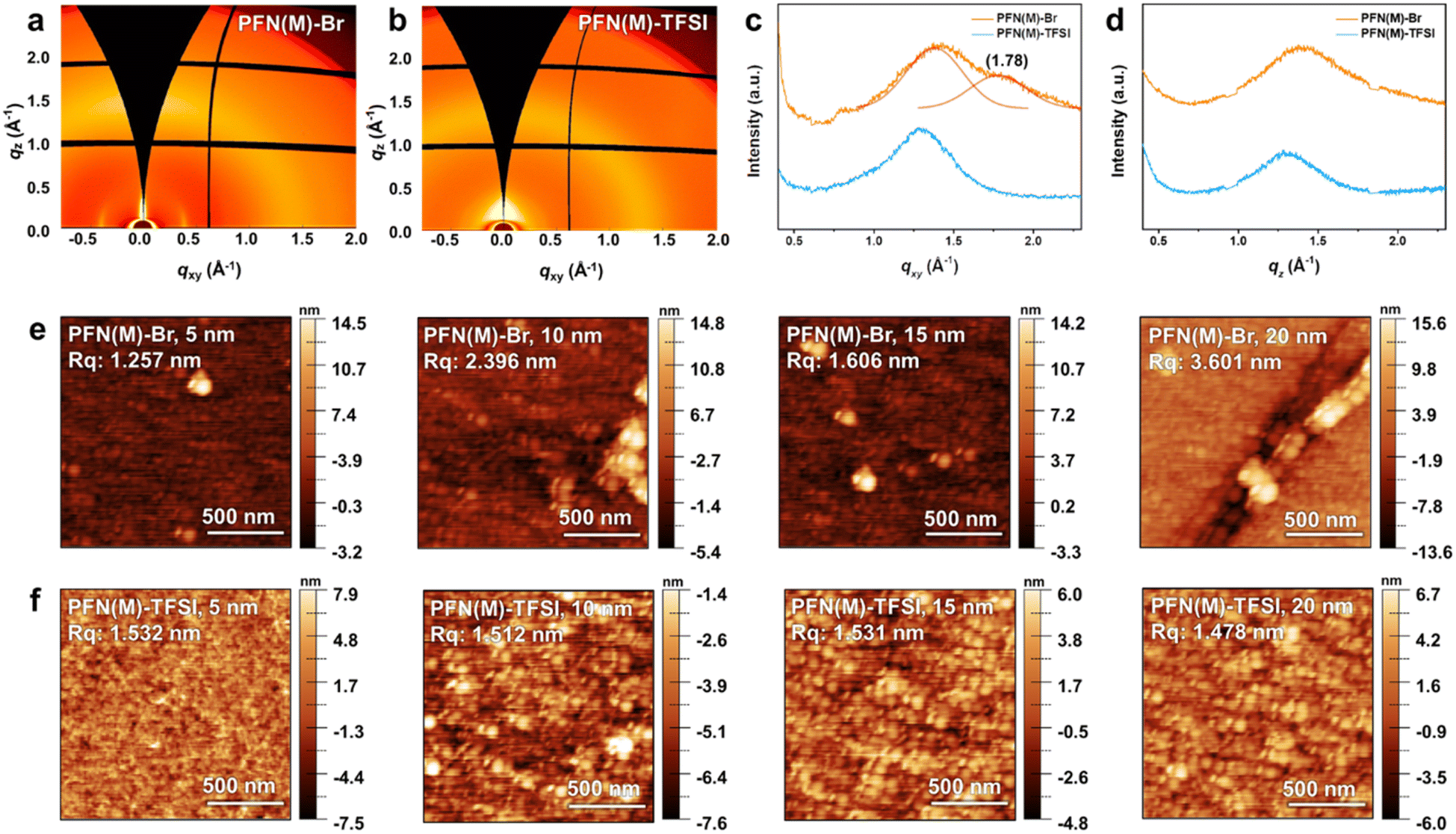 | ||
| Fig. 4 Microstructural analysis of (a) PFN(M)-Br, (b) PFN(M)-TFSI, and line-cut data of (c) in-plane and (d) out-of-plane directions extracted from GIWAXS images. The AFM image according to the thickness in a range of 5 to 20 nm for (e) PFN(M)-Br and (f) PFN(M)-TFSI. | ||
Atomic force microscopy (AFM) analysis was conducted to study the surface morphology. As shown in Fig. S6 and Table S1,† thicknesses of 5–20 nm were estimated based on the deposition conditions such as the concentration of the solutions and spin-coating methods. The surface images of PFN(M)-Br and PFN(M)-TFSI according to thickness are shown in Fig. 4e and f. In PFN(M)-Br, the surface image with a thickness of 5 nm shows aggregates, which increase as the thickness increases from 10 to 20 nm. In contrast, PFN(M)-TFSI shows an overall smooth film, and the root-mean-square roughness Rq values remain independent of the thickness.
In order to relate the film morphology and uniformity characteristics to vertical charge transport properties, the conductance values depending on the CIL thickness were calculated from the slope of J–V curves (Fig. 5a and b). The devices were vertically structured as ITO/CIL (5 nm, 10 nm, 15 nm, and 20 nm)/Al (100 nm). The conductance for 5 nm thick CILs, both PFN(M)-Br and PFN(M)-TFSI, exhibited an equal value of 0.041 S. It shows that the electron-extraction abilities for the thin CIL cannot be clearly distinguished. However, as the CIL thickness was getting thicker, the difference of conductance values between PFN(M)-Br and PFN(M)-TFSI became clear. For PFN(M)-Br, the conductance values were calculated to be 0.028 S and 0.017 S for 10 nm and 15 nm thicknesses, respectively, indicating that the charge transport ability degraded with increased thickness. On the other hand, the conductance values were calculated to be 0.041 S and 0.041 S for 10 nm and 15 nm thick PFN(M)-TFSI film layers, suggesting that the electrical properties for charge carrier extraction and transport were maintained until 15 nm thickness.
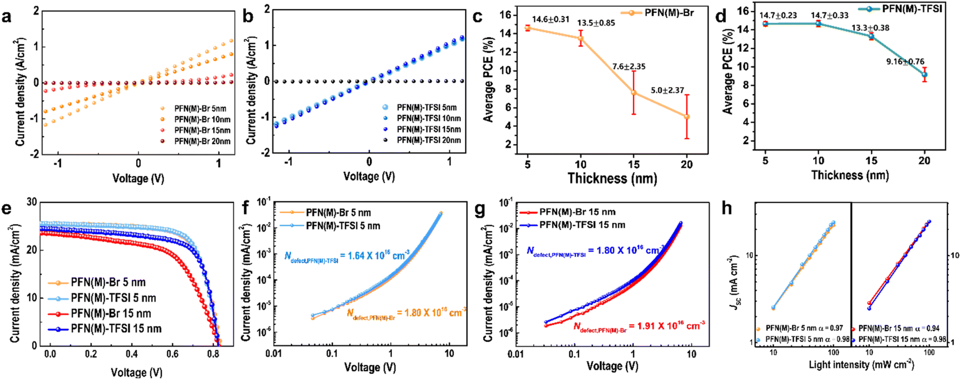 | ||
| Fig. 5 Dark J–V results according to the (a) PFN(M)-Br and (b) PFN(M)-TFSI thickness in a range of 5 nm to 20 nm with a 5 nm interval. Device efficiency distribution and the thickness-average efficiency graph with a standard deviation graph for 20 different devices with (c) PFN(M)-Br and (d) PFN(M)-TFSI as CILs. (e) The J–V curve for the maximum power conversion efficiency at a thickness of 5 nm and 15 nm for PFN(M)-Br and PFN(M)-TFSI CILs. The space charge limited current plot with the (f) 5 nm and (g) 15 nm thickness of PFN(M) series CIMs. (h) The light intensity–JSC curve of devices using 5 nm and 10 nm PFN(M)-Br and PFN(M)-TFSI. | ||
As shown in Fig. 3 and 4, the thicker PFN(M)-Br film has more amounts of aggregates leading to a non-uniform film state. Since the electrical properties in a thin film are possibly affected by the film morphology, the undesirable and excessive aggregates in the PFN(M)-Br film result in deficient charge transporting ability compared to the PFN(M)-TFSI film.58
We fabricated OPVs, using the PFN(M) series as the CIL, to confirm the effect of CIL thickness in the device performances (Fig. 5c, d and S7†). At a CIL thickness of 5 nm, PFN(M)-Br and PFN(M)-TFSI devices showed almost identical average power conversion efficiencies (PCEs) of 14.6% and 14.7%, respectively. However, PFN(M)-Br devices showed a decrease in average PCE starting from a thickness of 10 nm, and device reproducibility was significantly reduced. With 15 nm PFN(M)-Br, the average PCE decreases to 7.6%, by half of initial performance, indicating a severe thickness dependence of PFN(M)-Br. In addition, the range of the efficiency distribution was broadened with the increased thickness of PFN(M)-Br, which was attributed to the higher roughness and lower film flatness. In contrast, in the PFN(M)-TFSI devices, the only marginal change in the initial efficiency was observed until 15 nm thickness (14.7% to 13.3%). The PCE distribution in PFN(M)-TFSI based devices was also maintained in the CIL thickness range of 5–20 nm.
To conduct a more in-depth analysis of devices with CIL thicknesses, devices containing 5 nm and 15 nm thick CILs were chosen to represent thin and thick CIL devices, respectively (Fig. 5e and Table 2). At 5 nm thickness of the CIL, the best PCE of the PFN(M)-TFSI device (14.7%) is slightly improved compared to PFN(M)-Br devices (14.6%), which was attributed to the increase in the fill factor (FF). The favourable impact on charge transport contributes to desirable FF. At 15 nm, however, the best PCE of the PFN(M)-Br device decreases by 25%, primarily due to a decline of the FF. In contrast, in the PFN(M)-TFSI device, the PCE maintained 90% even under thick CIL conditions with marginal PCE variation.
| CIM | Thickness [nm] | J SC [mA cm−2] | Cal. JSCb [mA cm−2] | V OC [V] | FFd [%] | PCEe [%] |
|---|---|---|---|---|---|---|
| a Short circuit current density. b Calculated short circuit current density, obtained by external quantum efficiency measurement. c Open circuit voltage. d Fill factor. e Best power conversion efficiency and average power conversion efficiency of 20 different devices. | ||||||
| PFN(M)-Br | 5 | 25.5 | 25.1 | 0.83 | 70.9 | 15.0 (14.6) |
| 15 | 23.6 | 22.5 | 0.83 | 58.5 | 11.5 (7.6) | |
| PFN(M)-TFSI | 5 | 25.5 | 25.2 | 0.83 | 71.6 | 15.2 (14.7) |
| 15 | 24.9 | 23.5 | 0.83 | 69.2 | 14.1 (13.3) | |
Each value of short circuit current density (JSC) is evaluated by conducting external quantum efficiency measurement (Fig. S8†). The calculated values are 25.13 and 25.23 mA cm−2 for PFN(M)-Br and PFN(M)-TFSI at 5 nm, and 22.46 and 23.50 mA cm−2 at 15 nm, respectively. These integrated JSC values from EQE data are consistent with the JSC value in Table 2 with a reasonable margin of error, within 5%.
Space charge limited current measurement (SCLC) was conducted with electron-only devices to examine the density of trap states in devices (Fig. 5f and g). The densities of trap states in the interfacial area as well as in one single layer in devices are closely related to charge carrier transport and extraction properties. The calculated densities of trap states for 5 nm PFN(M)-Br and 5 nm PFN(M)-TFSI are 1.80 × 10¹⁶ and 1.64 × 1016 cm−3, respectively. When the CIL is thicker at 15 nm, the densities of trap states are calculated to be 1.91 × 1016 cm−3 and 1.80 × 1016 cm−3 for PFN(M)-Br and PFN(M)-TFSI, respectively. The lower trap density in thin and thick PFN(M)-TFSI based devices contributes to suppressed trap-assisted charge recombination in the devices and suggested fewer interfacial defects. Undesirable trap states in excessive aggregates in PFN(M)-Br might be induced, exhibiting the larger densities of trap states in the devices.
To further analyse the charge recombination characteristics depending on the different thicknesses of the CIL (5 nm and 15 nm), the JSC and open circuit voltage (VOC) of the devices were measured under different light intensities (P) from 10 to 100 mW cm−2 (Fig. 5h). It has been recognized that JSC is proportional to Pα, and the slope (α) becomes closer to unity when bimolecular recombination is suppressed. In thin thick CIL based devices, the α values are almost the same, exhibiting α = 0.97 and α = 0.98 for PFN(M)-Br and PFN(M)-TFSI, respectively. When the CIL is thicker, the α value severely decreased from 0.97 to 0.94 in PFN(M)-Br based devices; however, the α value remained stable in thick PFN(M)-TFSI based devices. The presence of thick PFN(M)-Br CIL led to increased susceptibility to bimolecular recombination, whereas PFN(M)-TFSI demonstrated relatively low sensitivity to bimolecular recombination during device operations.
The possibility of scalable application was evaluated using AFM (Fig. 6a, b and S9–S15†). The sample size was increased from 0.25 to 1, 9, and 25 cm2 for confirming that Rq remained constant along the diagonal line. In PFN(M)-Br, the average deviation of Rq was >1.03 nm even in a 1 cm2 area, which is inappropriate for scalable applications. In contrast, PFN(M)-TFSI showed a constant distribution of Rq with 0.17 nm average deviation in a 1 cm2 area. Even when the area enlarged to 25 cm2, the average deviation was <0.15 nm. This result presents the possibility of scalable application of PFN(M)-TFSI.
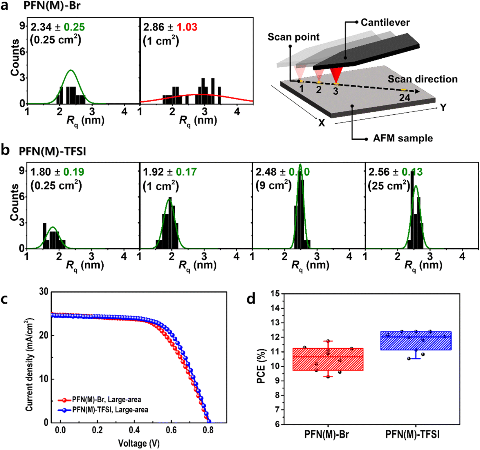 | ||
Fig. 6 The distribution of Rq values at 24 different scan points along the diagonal line in the area from 0.25 to 100 cm2. The  functions for (a) PFN(M)-Br and (b) PFN(M)-TFSI films. The values of functions for (a) PFN(M)-Br and (b) PFN(M)-TFSI films. The values of  functions are [average] ± [standard deviation] nm. (c) The J–V curve of large-area devices, which used PFN(M)-Br and PFN(M)-TFSI as CILs, and (d) the histograms of power conversion efficiency for 10 different devices. functions are [average] ± [standard deviation] nm. (c) The J–V curve of large-area devices, which used PFN(M)-Br and PFN(M)-TFSI as CILs, and (d) the histograms of power conversion efficiency for 10 different devices. | ||
Large-area devices were fabricated to realize the scalable application (Fig. 6c, d and Table S2†). As a result of fabricating 10 different devices for an area of 1.12 cm2, the average PCE value was 11.7% in the device using the PFN(M)-Br CIL and 12.4% in the device using the PFN(M)-TFSI CIL. The increased PCE of PFN(M)-TFSI compared to PFN(M)-Br is attributed to the more favourable film morphology associated with the amorphous nature of PFN(M)-TFSI. In addition, to verify the effectiveness of PFN(M)-TFSI as a CIL in large-area devices, we compared the device results using the PFN(E)-Br CIL, which is commercially available (Fig. S16 and Table S2†). As a result, the PCE distribution histogram also confirms that PFN(M)-TFSI was superior to PFN(M)-Br and PFN(E)-Br in scalable applications.
Furthermore, we also verified PFN(M)-TFSI as a CIL when utilizing various active materials. Fig. S17 and Table S3† present the J–V curves and PCE distribution graph with average standard deviation values of OPVs fabricated with PM6:L8-BO and D18:Y6 active layers. In the PM6:L8-BO system, the PFN(M)-TFSI based OPV showed a PCE of 16.4% with 5 nm and 14.1% with 15 nm. On the other hand, the PCE of the PFN(M)-Br based device decreased from 16.1% to 12.3%. Additionally, in the D18:Y6 system, a high PCE of 16.9% was achieved with PFN(M)-TFSI as the CIL and it remained at 16.3% with 15 nm thickness of PFN(M)-TFSI. However, the PFN(M)-Br based device showed decreased PCE from 16.6% to 12.9% when PFN(M)-Br was thicker. The effectiveness of PFN(M)-TFSI as a CIL was verified regardless of the blend active systems.
Conclusions
In this study, a novel PFN-moiety based CIM was synthesized by substituting anions of Br− with TFSI−. Compared to the generally used PFN(E)-Br, PFN(E)-TFSI showed poor solubility in methanol due to a stronger dipole interaction between the TFSI anion and the tertiary ammonium cation. The modified PFN(M)-TFSI was well soluble in methanol, and the increased anion size of TFSI− compared to Br− induced lower interchain interactions, which was confirmed by temperature dependent UV-Vis and 2D-GIWAXS. As a result, smoother film formation was achieved with PFN(M)-TFSI due to its amorphous nature. Based on PFN(M)-TFSI as the CIL, the distribution of device efficiency was shallower for all thicknesses ranging from 5 to 20 nm, compared to PFN(M)-Br. The thickness tolerance of PFN(M)-TFSI also enabled the possibility of scalable application, as revealed by the large-area AFM and device results.Conflicts of interest
There are no conflicts to declare.Acknowledgements
The 2D-GIWAXS measurements were conducted in the Pohang Accelerator Laboratory (PAL), Korea, with a synchrotron radiation of the 9A beamline. This work was supported by the National Research Foundation of Korea (NRF) (No. 2021R1A2C3004420 and 2020M3H4A1A02084908) and the Ministry of Trade, Industry and Energy (MOTIE 20006400).References
- Q. Kang, Z. Zheng, Y. Zu, Q. Liao, P. Bi, S. Zhang, Y. Yang, B. Xu and J. Hou, Joule, 2021, 5, 646–658 CrossRef CAS.
- D. Wang, R. Qin, G. Zhou, X. Li, R. Xia, Y. Li, L. Zhan, H. Zhu, X. Lu and H. L. Yip, Adv. Mater., 2020, 32, 2001621 CrossRef CAS PubMed.
- X. Huang, L. Zhang, Y. Cheng, J. Oh, C. Li, B. Huang, L. Zhao, J. Deng, Y. Zhang and Z. Liu, Adv. Funct. Mater., 2022, 32, 2108634 CrossRef CAS.
- Z. Chen, W. Song, K. Yu, J. Ge, J. Zhang, L. Xie, R. Peng and Z. Ge, Joule, 2021, 5, 2395–2407 CrossRef CAS.
- J. Noh, G.-U. Kim, S. Han, S. J. Oh, Y. Jeon, D. Jeong, S. W. Kim, T.-S. Kim, B. J. Kim and J.-Y. Lee, ACS Energy Lett., 2021, 6, 2512–2518 CrossRef CAS.
- C. Han, J. Wang, S. Zhang, L. Chen, F. Bi, J. Wang, C. Yang, P. Wang, Y. Li and X. Bao, Adv. Mater., 2023, 35, 2208986 CrossRef CAS PubMed.
- J. Kim, J. Park, D. Song, J. Jee, T. Gokulnath, S. C. Han, S.-H. Jin and J. W. Lee, Macromol. Res., 2023, 1–9 Search PubMed.
- Z. Abbas, S. U. Ryu, M. Haris, C. E. Song, H. K. Lee, S. K. Lee, W. S. Shin, T. Park and J.-C. Lee, Nano Energy, 2022, 101, 107574 CrossRef CAS.
- G. Zeng, W. Chen, X. Chen, Y. Hu, Y. Chen, B. Zhang and Y. Li, J. Am. Chem. Soc., 2022, 144(19), 8658–8668 CrossRef CAS PubMed.
- Y. Chen, J. Wan, G. Xu, X. Wu, X. Li, Y. Shen and Y. Li, Sci. China: Chem., 2022, 65, 1164–1172 CrossRef CAS.
- H. Chen, R. Zhang, X. Chen, G. Zeng, L. Kobera, S. Abbrent and Y. Li, Nat. Energy, 2021, 6, 1045–1053 CrossRef CAS.
- B. Zhang, F. Yang, S. Chen, H. Chen, G. Zeng, Y. Shen and Y. Li, Adv. Funct. Mater., 2022, 32, 2202011 CrossRef CAS.
- D. H. Lee, D. H. Kim, T. Kim, D. C. Lee, S. Cho and T. Park, Nano Energy, 2022, 93, 106878 CrossRef CAS.
- M. Kim, Y. Choi, D. Hwan Lee, J. Min, Y. J. Pu and T. Park, ChemSusChem, 2021, 14, 3475–3487 CrossRef CAS PubMed.
- Y. Choi, S. A. Park, Y. Bae, D. Kim, M. Kim and T. Park, Adv. Opt. Mater., 2023, 11, 2201788 CrossRef CAS.
- F. Pan, C. Sun, Y. Li, D. Tang, Y. Zou, X. Li, S. Bai, X. Wei, M. Lv and X. Chen, Energy Environ. Sci., 2019, 12, 3400–3411 RSC.
- J. Yao, B. Qiu, Z.-G. Zhang, L. Xue, R. Wang, C. Zhang, S. Chen, Q. Zhou, C. Sun and C. Yang, Nat. Commun., 2020, 11, 2726 CrossRef CAS PubMed.
- C. Chen, P. Xue, H. Lu, J. Wang, B. Jia, Y. Li, D. Qin, Y. Lin and X. Zhan, Energy Technol., 2021, 9, 2100281 CrossRef CAS.
- G.-W. Kim, Y. Choi, H. Choi, J. Min, T. Park and S. Song, J. Mater. Chem. A, 2020, 8, 21721–21728 RSC.
- Z. He, H. Wu and Y. Cao, Adv. Mater., 2014, 26, 1006–1024 CrossRef CAS PubMed.
- H. Ishii, K. Sugiyama, E. Ito and K. Seki, Adv. Mater., 1999, 11, 605–625 CrossRef CAS.
- R. Po, C. Carbonera, A. Bernardi and N. Camaioni, Energy Environ. Sci., 2011, 4, 285–310 RSC.
- M. M. Byranvand, T. Kim, S. Song, G. Kang, S. U. Ryu and T. Park, Adv. Energy Mater., 2018, 8, 1702235 CrossRef.
- S. Song, R. Hill, K. Choi, K. Wojciechowski, S. Barlow, J. Leisen, H. J. Snaith, S. R. Marder and T. Park, Nano Energy, 2018, 49, 324–332 CrossRef CAS.
- L.-M. Chen, Z. Xu, Z. Hong and Y. Yang, J. Mater. Chem., 2010, 20, 2575–2598 RSC.
- H. Ma, H. L. Yip, F. Huang and A. K. Y. Jen, Adv. Funct. Mater., 2010, 20, 1371–1388 CrossRef CAS.
- S. Bishnoi, R. Datt, S. Arya, S. Gupta, R. Gupta, W. C. Tsoi, S. N. Sharma, S. P. Patole and V. Gupta, Adv. Mater. Interfaces, 2022, 9, 2101693 CrossRef CAS.
- J. Choi, S. Song, M. T. Hörantner, H. J. Snaith and T. Park, ACS Nano, 2016, 10, 6029–6036 CrossRef CAS PubMed.
- F. Huang, H. Wu, D. Wang, W. Yang and Y. Cao, Chem. Mater., 2004, 16, 708–716 CrossRef CAS.
- J. Luo, H. Wu, C. He, A. Li, W. Yang and Y. Cao, Appl. Phys. Lett., 2009, 95, 043301 CrossRef.
- D. Lv and D. Liu, Sol. RRL, 2023, 7, 230699 Search PubMed.
- Q. Chen, C. Wang, Y. Li and L. Chen, J. Am. Chem. Soc., 2020, 142, 18281–18292 CrossRef CAS PubMed.
- B. H. Lee, I. H. Jung, H. Y. Woo, H. K. Shim, G. Kim and K. Lee, Adv. Funct. Mater., 2014, 24, 1100–1108 CrossRef CAS.
- C. Feng, X. Wang, Z. He and Y. Cao, Sol. RRL, 2021, 5, 2000753 CrossRef CAS.
- L. Chen, C. Xie and Y. Chen, Org. Electron., 2013, 14, 1551–1561 CrossRef CAS.
- J. H. Seo and T.-Q. Nguyen, J. Am. Chem. Soc., 2008, 130, 10042–10043 CrossRef CAS PubMed.
- G.-W. Kim, D. V. Shinde and T. Park, RSC Adv., 2015, 5, 99356–99360 RSC.
- K. Zhang, Z. Hu, C. Sun, Z. Wu, F. Huang and Y. Cao, Chem. Mater., 2017, 29, 141–148 CrossRef CAS.
- X. Liu, B. Xie, C. Duan, Z. Wang, B. Fan, K. Zhang, B. Lin, F. J. Colberts, W. Ma and R. A. Janssen, J. Mater. Chem. A, 2018, 6, 395–403 RSC.
- X. Lin, Y. Wang, J. Wu, Z. Tang, W. Lin, L. Nian and G. Yi, ACS Appl. Energy Mater., 2021, 4, 5905–5912 CrossRef CAS.
- J. Gao, J. Wang, C. Xu, Z. Hu, X. Ma, X. Zhang, L. Niu, J. Zhang and F. Zhang, Sol. RRL, 2020, 4, 2000364 CrossRef CAS.
- K. Zhang, Z. Chen, A. Armin, S. Dong, R. Xia, H. L. Yip, S. Shoaee, F. Huang and Y. Cao, Sol. RRL, 2018, 2, 1700169 CrossRef.
- J. Faisst, E. Jiang, S. Bogati, L. Pap, B. Zimmermann, T. Kroyer, U. Würfel and M. List, Sol. RRL, 2023, 7, 2300663 CrossRef CAS.
- G. Xu, L. Gao, H. Xu, L. Huang, Y. Xie, X. Cheng, Y. Li, L. Chen and Y. Chen, J. Mater. Chem. A, 2017, 5, 13807–13816 RSC.
- P. Cai, C. Song, S. Lei, K. Yu, L. Ding, D. Wang, G. Chen, H. Peng, B. Li and X. Wang, J. Mater. Chem. A, 2023, 11, 18723–18732 RSC.
- J. Fang, Z. Zhang, Z. Zhang, Y. Han, D. Xia, C. Zhao, Y. Zhang, L. Wang, C. Xiao and S. You, J. Mater. Chem. A, 2023, 11, 6574–6580 RSC.
- Z. Chen, Z. Hu, Z. Wu, X. Liu, Y. Jin, M. Xiao, F. Huang and Y. Cao, J. Mater. Chem. A, 2017, 5, 19447–19455 RSC.
- R. Yang, A. Garcia, D. Korystov, A. Mikhailovsky, G. C. Bazan and T.-Q. Nguyen, J. Am. Chem. Soc., 2006, 128, 16532–16539 CrossRef CAS PubMed.
- S. D. Collins, O. V. Mikhnenko, T. L. Nguyen, Z. D. Rengert, G. C. Bazan, H. Y. Woo and T. Q. Nguyen, Adv. Electron. Mater., 2017, 3, 1700005 CrossRef.
- L. Liu, R. Kou and G. Liu, Soft Matter, 2017, 13, 68–80 RSC.
- D. Mecerreyes, Prog. Polym. Sci., 2011, 36, 1629–1648 CrossRef CAS.
- Q.-N. Zhu, Q. Wang, Y.-B. Hu and X. Abliz, Molecules, 2019, 24, 1346 CrossRef PubMed.
- K. Choi, D. H. Lee, W. Jung, S. Kim, S. H. Kim, D. Lee, S. Song and T. Park, Adv. Funct. Mater., 2022, 32, 2112027 CrossRef CAS.
- P. Brocorens, A. Van Vooren, M. L. Chabinyc, M. F. Toney, M. Shkunov, M. Heeney, I. McCulloch, J. Cornil and R. Lazzaroni, Adv. Mater., 2009, 21, 1193–1198 CrossRef CAS.
- Y. Xi, C. M. Wolf and L. D. Pozzo, Soft Matter, 2019, 15, 1799–1812 RSC.
- D. Niedzialek, V. Lemaur, D. Dudenko, J. Shu, M. R. Hansen, J. W. Andreasen, W. Pisula, K. Müllen, J. Cornil and D. Beljonne, Adv. Mater., 2013, 25, 1939–1947 CrossRef CAS PubMed.
- J.-W. Ha, J. G. Jung, D. H. Ryu, S. Lee, C. E. Song, B. Lim, Y. J. Jung, J. M. Park and D.-H. Hwang, Macromol. Res., 2023, 31, 25–31 CrossRef CAS.
- X. Cao, H. Li, J. Hu, H. Tian, Y. Han, B. Meng, J. Liu and L. Wang, Angew. Chem., Int. Ed., 2023, 62, e202212979 CrossRef CAS PubMed.
Footnotes |
| † Electronic supplementary information (ESI) available. See DOI: https://doi.org/10.1039/d4ta00044g |
| ‡ Yurim Bae and Jeongsu Kim contributed equally to this work. |
| This journal is © The Royal Society of Chemistry 2024 |