
 Open Access Article
 This Open Access Article is licensed under a
 Creative Commons Attribution 3.0 Unported Licence
Molecular modification of spiro[fluorene-9,9′-xanthene]-based dopant-free hole transporting materials for perovskite solar cells†
Vinay
Kumar‡
ab,
Deepak
Kumar‡
ab,
Rohit D.
Chavan‡§
 c,
Kodali Phani
Kumar
ab,
Bommaramoni
Yadagiri
ab,
Muhammad
Ans
c,
Joanna
Kruszyńska
c,
Apurba
Mahapatra
c,
Jan
Nawrocki
c,
Kostiantyn
Nikiforow
c,
Nada
Mrkyvkova
de,
Peter
Siffalovic
de,
Pankaj
Yadav
fg,
Seckin
Akin
h,
Surya Prakash
Singh
*ab and
Daniel
Prochowicz
*c
c,
Kodali Phani
Kumar
ab,
Bommaramoni
Yadagiri
ab,
Muhammad
Ans
c,
Joanna
Kruszyńska
c,
Apurba
Mahapatra
c,
Jan
Nawrocki
c,
Kostiantyn
Nikiforow
c,
Nada
Mrkyvkova
de,
Peter
Siffalovic
de,
Pankaj
Yadav
fg,
Seckin
Akin
h,
Surya Prakash
Singh
*ab and
Daniel
Prochowicz
*c
aDepartment of Polymer and Functional Material, CSIR-Indian Institute of Chemical Technology (IICT), Uppal Road, Tarnaka, Hyderabad-500007, India. E-mail: spsingh@iict.res.in
bAcademy of Scientific and Innovative Research (AcSIR), Ghaziabad-201002, India
cInstitute of Physical Chemistry, Polish Academy of Sciences, Kasprzaka 44/52, 01-224 Warsaw, Poland. E-mail: dprochowicz@ichf.edu.pl
dInstitute of Physics, Slovak Academy of Sciences, Dubravska cesta 9, 84511 Bratislava, Slovakia
eCenter for Advanced Materials and Applications, Slovak Academy of Sciences, Dubravska cesta 9, 84511 Bratislava, Slovakia
fDepartment of Solar Energy, School of Energy Technology, Pandit Deendayal Energy University, Gandhinagar-382 007, Gujarat, India
gDepartment of Physics, School of Energy Technology, Pandit Deendayal Energy University, Gandhinagar-382 007, Gujarat, India
hDepartment of Metallurgical and Materials Engineering, Necmettin Erbakan University, Konya, 42090, Turkey
First published on 20th February 2024
Abstract
The molecular engineering of organic hole-transporting materials (HTMs) plays an important role in enhancing the performance and stability of perovskite solar cells (PSCs) as well as reducing their fabrication cost. Here, two low-cost spiro-OMeTAD analogues, namely SP-Naph and SP-SMe, featuring a spiro[fluorene-9,9-xanthene] (SFX) central core and asymmetric subunits are designed and synthesized. Specifically, the SFX core in the SP-Naph molecule is substituted with dimethoxyphenylnaphthylamine subunits to enhance conductivity and charge transport properties by expansion of the π-conjugated structure. On the other hand, in the molecular structure of SP-SMe, the methoxy groups (–OMe) from diphenylamine units were partially replaced with the methylsulfanyl groups (–SMe) to increase interaction with the perovskite surface through the “Lewis soft” S atoms. By combining various experimental and simulation methods, thestructure–property relationship of the newly synthesized HTMs was thoroughly investigated. The suitable HOMO energy level with the perovskite layer together with superior photoelectric properties and enhanced thermostability and humidity resistivity are obtained for the SP-SMe HTM. As a result, the planar n–i–p PSC with the dopant-free SP-SMe HTM yields a maximum power conversion efficiency (PCE) of 21.95%, which outperforms that with SP-Naph (20.51%) and doped spiro-OMeTAD (19.23%). Importantly, the device with SP-SMe also reveals enhanced operational stability under continuous 1 sun illumination and thermal stability at 65 °C. These findings provide valuable insight for the rational design of dopant-free organic HTMs based on the SFX core, which would promote the development of highly efficient and stable devices.
1 Introduction
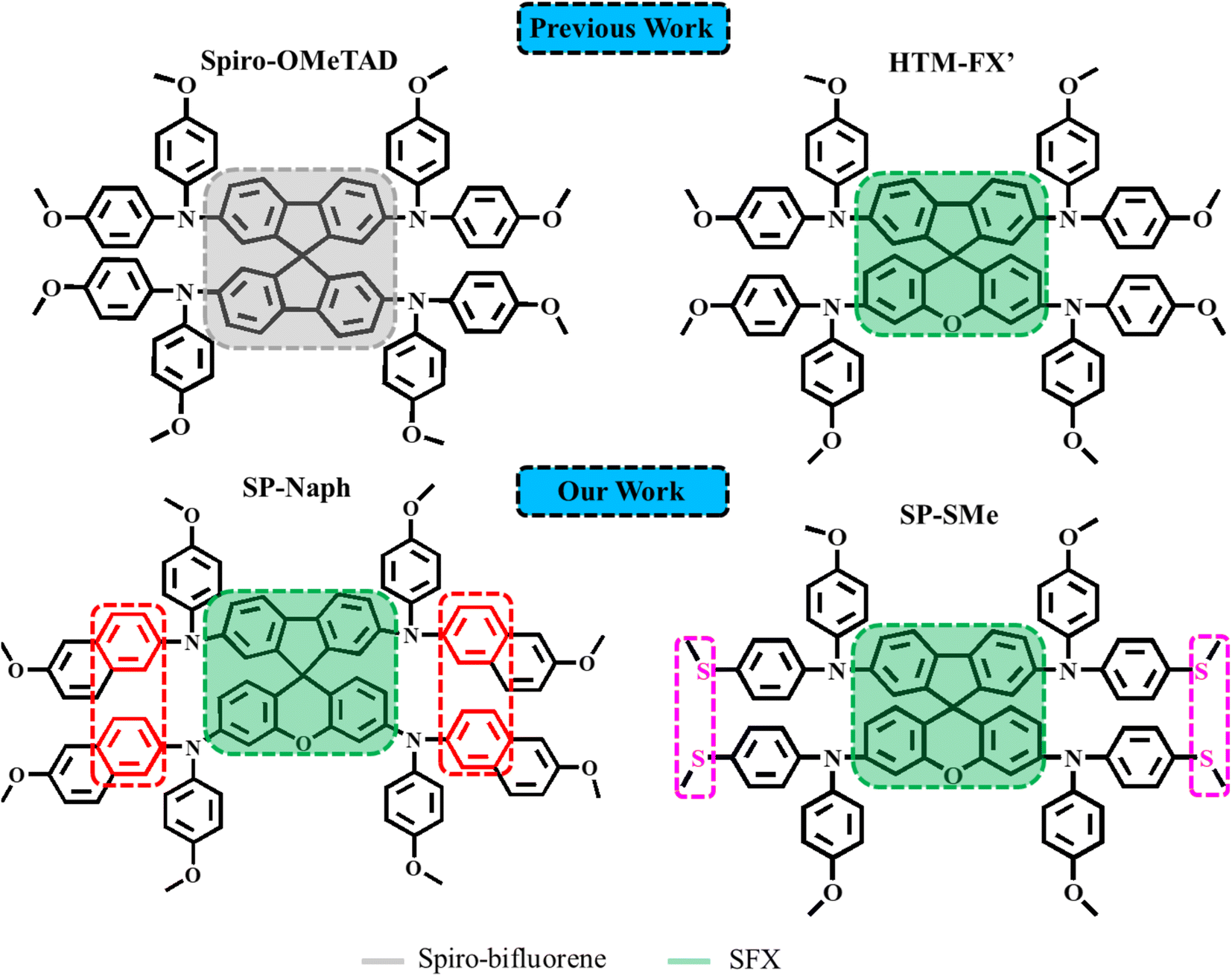
Perovskite solar cells (PSCs) have recently attracted great attention in the photovoltaic field due to their outstanding power conversion efficiency (PCE) exceeding 26%, which has been achieved for single-junction devices.1 Despite achieving fast progress in PCEs, the long-term stability of PSCs is still the major bottleneck towards their commercialization for outdoor applications.2–4 There are several extrinsic factors that limit the devices' stability such as moisture,5,6 oxygen,7 high temperature,8,9 and UV light exposure.10 In addition, intrinsic properties of the perovskite active materials under stresses of operational conditions (light illumination, electric field, and heat) can also affect the stability of PSCs.11In the last couple of years, an extensive effort has been made in order to tackle the above-mentioned stability issues by modifying each component of the device.12 The stability of the perovskite absorber layer can be improved by its surface passivation using various materials,13–15 and compositional engineering,16–18 and by adding hydrophobic additives.19,20 To achieve highly stable and efficient PSCs, the quality of electron and hole transport layers also plays a vital role.21 For regular n–i–p device configuration, titanium dioxide (TiO2) is the most widely used electron transport layer (ETL) in PSCs.22 Due to its low conductivity, poor ultraviolet stability and high surface defect density, modification of TiO2 by metal doping, interface engineering and forming nanocomposites has been applied to improve the stability of TiO2-based PSCs.23–25 Alternatively, the use of other metal oxides in the form of colloidal SnO2 or nanocrystalline ZnO has been proposed to not only facilitate the electron extraction and transport but also to achieve more efficient and stable ETLs than TiO2.26–30 These semiconducting materials could be further modified by metal ion doping, additive engineering, surface modification and forming multiple ETLs to maintain long-term stability under the operation conditions.31–34 In the case of hole transport materials (HTMs), much effort has been devoted to replacing the most commonly used 2,2′,7,7′-tetrakis(N,N-di-p-methoxyphenylamine)-9,9′-spirobifluorene (spiro-OMeTAD), which not only suffers from expensive and tedious synthesis but also low stability under thermal stress.35–39 In addition, the spiro-OMeTAD film exhibits moderate hole conductivity and mobility without additional dopants such as bis(trifluoromethane)sulfonimide lithium salt (Li-TFSI) and 4-tert-butylpyridine (t-BP). However, the presence of these dopants can cause deterioration of device stability due to their hygroscopic and volatile nature.40,41
The molecular structure of spiro-OMeTAD comprises a 9.9′-spirobifluorene core and four p,p′-dimethoxydiphenylamine units (Scheme 1). The optical and electronic properties of spiro-OMeTAD could be tuned by changing the positions of two –OMe substituents or their donating ability. Jeon et al., reported that changing one para-OMe substituent to the ortho-position is favorable for a higher fill factor of PSCs.42 In turn, the replacement of –OMe groups with methylsulfanyl (–SMe) resulted in a deeper HOMO energy level than spiro-OMeTAD, promoting charge extraction from the perovskite layer.43 Due to the complex and multistep synthesis routes of spirobifluorene-type HTMs, intense research has focused on developing low-cost and efficient HTM alternatives. In this context, spiro[fluorene-9,9-xanthene] (SFX) has been proposed as a core moiety, which can be readily prepared via a two-step synthetic reaction using inexpensive starting materials with a high overall yield.44–47 By molecular engineering of the SFX-core with various diphenylamine units, the performances higher than the PCEs of the reference devices based on spiro-OMeTAD were reported. For example, Chiykowski, et al. implemented an SFX-based material (namely HTM-FX′, Scheme 1) in planar n–i–p PSCs and achieved a high PCE of 20.8%, outperforming that with spiro-OMeTAD (20.4%).48 However, to the best of our knowledge, the reported SFX-based HTMs require the use of dopants (LiTFSI and t-BP), which are believed to be detrimental to long-term device stability.
 | ||
| Scheme 1 Molecular structure representations of spiro-OMeTAD, HTM-FX′, SP-Naph and SP-SMe HTMs. | ||
For the development of new organic HTMs, it is necessary to pay attention to the change in the chemical structure and to the intermolecular interactions, which play an important role in promoting charge transport properties. Herein, we disclose the design and synthesis of new molecules based on the SFX-core, denoted as SP-Naph and SP-SMe (Scheme 1), for the purpose of creating low-cost dopant-free HTMs toward stable and efficient PSCs. The SP-Naph molecule was designed to feature an asymmetrically substituted SFX-core with dimethoxyphenylnaphthylamines, which are assumed to tune its electrical properties, π-conjugation length and intermolecular interactions due to the larger area of naphthyl rings than phenyl groups. In the case of the molecular structure of SP-SMe, methoxy groups from diphenylamine units were partially replaced with the methylsulfanyl groups (SMe). The introduction of SMe groups is expected to enhance hole extraction properties by providing better band alignment with the perovskite layer and passivate its surface defects by forming stronger molecular interaction with the undercoordinated Pb2+ (S atoms are softer Lewis base than O atoms). The effects of molecular engineering of the SFX-core on the intermolecular interactions, charge-extraction ability and recombination kinetics within the device are theoretically and experimentally investigated. The devices with a planar n–i–p architecture based on dopant-free SP-Naph and SP-SMe HTLs were found to be capable of yielding a high PCE of 20.51% and 21.95%, respectively, which were higher than that measured for our doped spiro-OMeTAD based PSCs (19.23%). In addition, these devices also exhibit superior environmental, thermal and illumination stability compared to spiro-OMeTAD-based cells.
2 Results and discussion
SP-Naph and SP-SMe were synthesized by simple three-step procedures and synthesis details are illustrated in the Experimental section. Specifically, SP-Naph and SP-SMe HTMs were synthesized through the Buchwald–Hartwig C–N cross-coupling reaction between TBX, I and DOS using Pd2(dba)3 as a catalyst as shown in Schemes S1 and S2.† The chemical structures of SP-SMe and SP-Naph were confirmed by 1H NMR, 13C NMR and MALDI-TOF characterization (Fig. S1–S15).† Based on our cost analysis (see Note 1 in the ESI†), it is evident that these HTMs are significantly more cost-effective when compared to the commercially available spiro-OMeTAD. The cost of SP-SMe and SP-Naph is 1/21st and 1/12th of the price of the purified spiro-OMeTAD (priced at $565 per gram with high purity from Sigma/Merck), respectively.It is expected that the partial modification of diphenylamine (DPA) motifs in HTM-FX′ can alter its electrical conductivity and energy levels. Fig. S16† shows the current–voltage (I–V) relations of ITO/HTM/Au films, from the slope of which we can calculate conductivity (σ0). The calculated σ0 for HTM-FX′ is 5.94 × 10⁻⁶ S cm−1, which is higher than that of the undoped spiro-OMeTAD film (2.50 × 10⁻⁷ S cm−1).49 The presence of the naphthyl subunit greatly enhances the electrical conductivity of the SP-Naph film (6.41 × 10⁻⁶ S cm−1) due to the expansion of the π-conjugated structure.50 The partial replacement of the –OMe on the benzene moiety (HTM-FX′) with the –SMe group (SP-SMe) also enhances its conductivity (6.94 × 10⁻⁶ S cm−1) due to less electronegativity of the S atom.50 The conductivity along its slope is summarized in Table S1.† To gain further insight into the effect of the modified DPA motif in HTM-FX′ on the electronic properties, we modelled the Frontier molecular orbitals (FMOs) using the density functional theory (DFT). The calculated electron cloud density distributions of the HOMO and LUMO for all investigated HTMs are shown in Fig. 1a. In HTM-FX′, HOMO density is uniformly distributed on the entire fluorene and DPA units, while LUMO density mostly covered the fluorine unit with less distribution towards DPA units. The HOMO density of SP-Naph is localized mainly on the phenylnaphthylamine unit, while the LUMO density is located on the fluorene unit as well as on the –OMe groups in the phenylnaphthylamine unit. Therefore, the phenylnaphthylamine unit in SP-Naph can participate in the charge carrier transport, which reflects better conductivity and lower HOMO value than that found in HTM-FX′. In contrast, the HOMO density in SP-SMe is distributed on the full central unit (fluorene and xanthene) as compared to HTM-FX′ and SP-Naph, while LUMO density is spread over the fluorene unit along with –SMe groups. These DFT calculations show that SP-SMe is expected to have better hole transporting ability due to overlaps between the HOMO and LUMO and stronger donor ability of S atoms, which alter the HOMO density.51
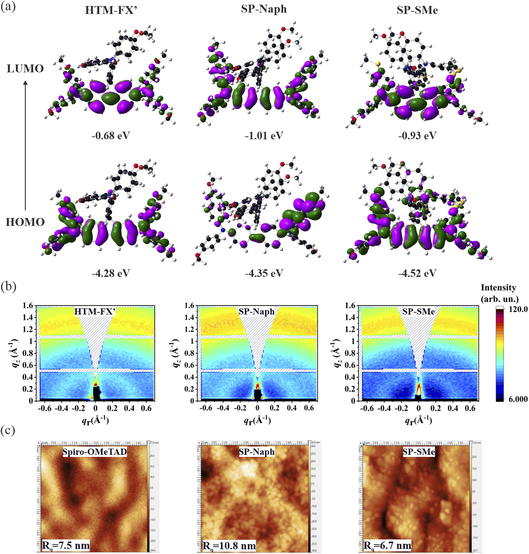 | ||
| Fig. 1 (a) HOMO–LUMO density of HTM-FX′, SP-Naph and SP-SMe HTMs based on DFT calculations. (b) GIWAXS plots of the spin-coated HTMs on the native Si substrate. (c) 2D AFM topography images of the perovskite/HTL films. | ||
In the following, we will focus on the electronic and structural properties of SP-SMe and SP-Naph HTMs and compare them to a thoroughly investigated HTM-FX′-based sample.48 First, cyclic voltammetry (CV) measurements were performed for SP-Naph and SP-SMe HTMs to estimate their energy levels experimentally (Fig. S17†). Electrochemical properties of HTM-FX′ have been previously reported by Chiykowski et al., and its HOMO value was found to be −5.16 eV.48 In turn, the HOMO energy levels of SP-Naph and SP-SMe are estimated to equal to −5.28 eV and −5.36 eV, respectively, which are consistent with the DFT calculation trend. The LUMO levels can be deduced by adding the optical band gaps (Eg) of these HTMs to the HOMO levels. The UV-vis spectra of HTM solutions in toluene as well as in the form of thin films are presented in Fig. S18.† All HTMs show bimodal absorption and the absorption onset of SP-Naph exhibits a larger extent of red-shift, which may imply stronger intermolecular interaction and tighter molecular packing due to enhanced π–π stacking interactions.52 By subtracting the Eg values estimated from the corresponding absorption edges, the LUMO levels were calculated to be −2.31 eV for SP-Naph and −2.64 eV for SP-SMe (Table S2†). The energy levels of different HTMs relative to our perovskite composition are depicted in Fig. S19.† As seen, the lowered HOMO levels of SP-Naph and SP-SMe can ensure better hole extraction from the perovskite layer compared to HTM-FX′ and spiro-OMeTAD HTMs. Notably, a deeper lying HOMO level of SP-SMe is beneficial for better energetic matches with the perovskite to improve the Voc of the PSCs. Further, the molecular crystallographic structure of the HTM films was investigated by the grazing incident wide-angle X-ray scattering (GIWAXS). All three studied HTMs were spin-coated on the native Si substrates to prevent diffractions from the perovskite layer, which typically has a very high scattering cross-section and would significantly reduce the visibility of the molecular patterns. The thickness of the spin-coated layer was ∼173 ± 7 nm for each HTM. GIWAXS reciprocal space maps in Fig. 1b show two broad scattering peaks at q ∼0.45 Å−1 and ∼1.31 Å−1 (see Fig. S20 in the ESI†), originating from the molecular packing and intermolecular π–π stacking, respectively. All three investigated HTMs exhibit a mixture of amorphous and crystalline phases, while the individual crystalline domains show a random correlation in molecular orientation. Unfortunately, a significant amorphous background prevents accurate peak position, thus determining the exact molecular packing.
The SP-Naph HTM contains eight –OMe groups, while the SP-SMe HTM has four –OMe and four –SMe groups, which can potentially reduce trap-induced interfacial recombination by forming interaction with the undercoordinated Pb2+ in the perovskite film. Therefore, we performed electrostatic potential (ESP) surface analysis of the SP-Naph and SP-SMe HTMs to better understand which group is more prone to passivate the perovskite surface defects. The ESP maps of the investigated HTMs are shown in Fig. S21.† It is observed that the most electronegative potential is localized around S atoms in the SP-SMe, which may serve as Lewis base to passivate uncoordinated Pb2+ defects in the perovskite film. To support this statement, we also calculated the binding energies of O (SP-Naph) and S (SP-SMe) atoms with the perovskite surface (Fig. S22†). SP-SMe exhibited lower adsorption energy (−3.35 eV) on the undercoordinated Pb2+ site compared with SP-Naph (−2.62 eV), confirming that the –SMe group strongly passivates these defects (Table S3†). X-ray photoelectron spectroscopy (XPS) measurement was further performed to experimentally probe the chemical interaction of the perovskite/HTM interfaces (Fig. S23†). After spin-coating of thin layers of SP-Naph and SP-SMe on top of the perovskite layer, the shift of the Pb 4f core levels towards lower binding energies is observed compared to bare perovskite. In addition, the I 3d peaks exhibit a similar trend after depositing SP-SMe and SP-Naph. The higher shift in the perovskite/SP-SMe film indicates the stronger interaction between perovskite and the SP-SMe layer, which can suppress non-radiative recombination and improve device performance. Atomic force microscopy (AFM) images and the root mean square (Rq) values show that the surface of the SP-SMe on the perovskite film is smoother than that of SP-Naph and spiro-OMeTAD (Fig. 1c). The relative roughness of SP-SMe is only 6.7 nm, which is lower than the roughness of SP-Naph (10.8 nm) and spiro-OMeTAD (7.5 nm). The 3D AFM topography images have been depicted in Fig. S24.†
To evaluate the effect of dopant-free SP-Naph and SP-SMe HTMs, we fabricated devices with an n–i–p architecture of ITO/SnO2/perovskite/HTLs/Au (for the device fabrication details, see the Experimental section). The optimum concentration of SP-Naph and SP-SMe was found to be 15 mg mL−1 in a toluene solution in terms of champion efficiency (Fig. S25 and Table S4†), which is much lower than the concentration of spiro-OMeTAD (90 mg mL−1). The HTLs had a homogeneous coverage on the perovskite films (Fig. S26†). Fig. 2a shows the current–voltage (J–V) curves for the champion devices, while their corresponding photovoltaic metrics are summarized in Table 1. As seen, the device based on the SP-SMe HTM reaches a maximum PCE of 21.95% under AM 1.5G irradiation at 100 mW cm−2 with an open-circuit voltage (VOC) of 1.16 V, a short-circuit photocurrent (JSC) of 24.23 mA cm−2 and a fill factor (FF) of 77.65%. This performance was higher than that of the best SP-Naph-based device with a PCE of 20.51%. Our control device based on spiro-OMeTAD with and without dopants exhibits a PCE of 19.23% and 15.62%, respectively. We also tested HTM-FX′ as a dopant-free HTL with the same concentration (15 mg mL−1), however, the corresponding devices exhibit poor performance with a PCE below 5% (Fig. S27†). Next, the PCEs of the investigated devices were verified by measuring the steady-state power output at the maximum power point (MPP). As shown in Fig. 2b, the device with SP-SMe shows a higher and more stable output efficiency after 200 seconds of continuous illumination.
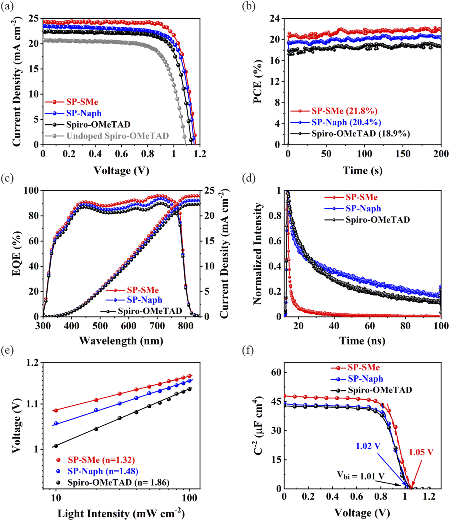 | ||
| Fig. 2 (a) J–V curves under the backward scan of the optimized devices based on undoped and doped spiro-OMeTAD, SP-SMe and SP-Naph HTMs. (b) Maximum power point (MPP) tracking for 200 s. (c) External quantum efficiency and integrated JSC. (d) TRPL spectra of the perovskite/HTL films. (e) VOC at different light intensities and (f) Mott–Schottky plots of the devices with different HTMs. | ||
| HTLs | V OC (V) | J SC (mA—m−2) | J SC (EQE) (mA—m−2) | FF (%) | PCE (%) | HI (%) | |
|---|---|---|---|---|---|---|---|
| Undoped spiro-OMeTAD | Champion | 1.08 | 20.64 | — | 70.11 | 15.62 | 10.75 |
| Spiro-OMeTAD | Champion | 1.13 | 22.50 | 22.29 | 75.27 | 19.23 | |
| Average | 1.12 ± 0.005 | 22.15 ± 0.3 | — | 73.46 ± 1.1 | 18.54 ± 0.4 | 5.14 | |
| SP-Naph | Champion | 1.15 | 23.45 | 23.10 | 75.73 | 20.51 | |
| Average | 1.14 ± 0.004 | 23.02 ± 0.2 | — | 74.14 ± 0.8 | 19.64 ± 0.4 | 2.87 | |
| SP-SMe | Champion | 1.16 | 24.23 | 23.95 | 77.65 | 21.95 | |
| Average | 1.16 ± 0.004 | 23.86 ± 0.2 | — | 76.51 ± 0.6 | 21.19 ± 0.3 | 1.86 |
The statistical analysis of photovoltaic parameters for 20 devices based on different HTMs is shown in Fig. S28.† It is observed that the enhanced performances of SP-SMe-based devices are due to higher values of VOC and FF. Furthermore, the devices based on SP-SMe also demonstrated negligible hysteresis effects, as evidenced by the forward and reverse scan curves shown in Fig. S29† (for the distribution of photovoltaic parameters, see Table S5†). These improvements could be attributed to the higher conductivity and more favorable band alignment of SP-SMe with the perovskite layer. In addition, the strong coordination of the S atom with the undercoordinated Pb2+ sites can suppress recombination at the interface. To validate the measured JSC values, we performed external quantum efficiency (EQE) measurements for the investigated devices. As shown in Fig. 2c, the calculated JSC values from integrating the EQE spectra confirm the JSC values determined from J–V analysis. The value of JSC for the SP-SMe-based device (23.95 mA cm—2) is higher than those of SP-Naph (23.84 mA cm—2) and spiro-OMeTAD (21.88 mA cm—2), likely due to its better charge extraction properties (vide infra).
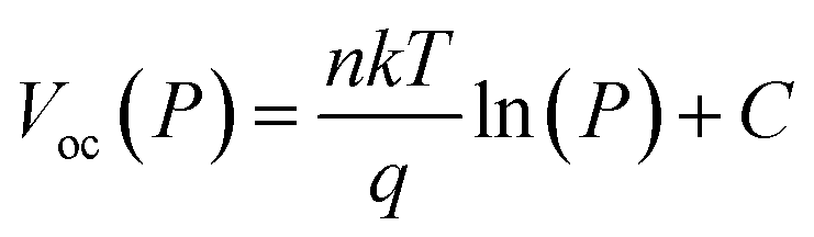
To evaluate the charge extraction ability of the investigated HTMs, steady-state photoluminescence (PL) and time-resolved photoluminescence (TRPL) measurements were conducted. Fig. S30† shows the PL spectra of the pristine perovskite and perovskite/HTM films. As seen, the PL intensities were significantly quenched for all modified perovskite films, especially when they are covered with the SP-SMe HTM, indicating its effective hole extraction and transfer capabilities. These results are in good agreement with the TRPL curves shown in Fig. 2d. We fitted the decay curves using the biexponential equation: (y = A1![[thin space (1/6-em)]](https://www.rsc.org/images/entities/char_2009.gif) exp(−x/τ1) + A2exp(−x/τ2) + y0), where τ1 and τ2 refer to the fast and slow decay associated with surface and bulk recombinations, respectively (Table S6†).53 The perovskite with SP-SMe showed a shorter charge carrier lifetime (τ1 = 0.6 ns, τ2 = 15 ns) than those of SP-Naph (τ1 = 1.8 ns, τ2 = 67 ns), and spiro-OMeTAD (τ1 = 6 ns, τ2 = 47 ns), which confirms efficient charge transfer between SP-SMe and the perovskite film. The improved charge transfer should be also beneficial in reducing the nonradiative recombination at the interface. The dependence of VOC on the incident light intensity in logarithmic form is commonly used to express the charge recombination process. The ideal factor (n) can be calculated by using the equation:
exp(−x/τ1) + A2exp(−x/τ2) + y0), where τ1 and τ2 refer to the fast and slow decay associated with surface and bulk recombinations, respectively (Table S6†).53 The perovskite with SP-SMe showed a shorter charge carrier lifetime (τ1 = 0.6 ns, τ2 = 15 ns) than those of SP-Naph (τ1 = 1.8 ns, τ2 = 67 ns), and spiro-OMeTAD (τ1 = 6 ns, τ2 = 47 ns), which confirms efficient charge transfer between SP-SMe and the perovskite film. The improved charge transfer should be also beneficial in reducing the nonradiative recombination at the interface. The dependence of VOC on the incident light intensity in logarithmic form is commonly used to express the charge recombination process. The ideal factor (n) can be calculated by using the equation:
As widely reported, the hygroscopic and volatile nature of chemical dopants in the traditional spiro-OMeTAD HTM can significantly hinder PSC stability.55 Therefore, the absence of these dopants in our HTLs could effectively improve the stability of PSCs. First, we studied the water permeability by measuring the static contact angle of water droplets on the surface of HTLs. The evolution of water contact angles on the perovskite/HTL films over time is shown in Fig. 3a–c. As seen, water contact angles of 75.40°, 78.23° and 87.49° were determined after 20 s for spiro-OMeTAD, SP-Naph and SP-SMe, respectively. The higher water contact angles of SP-Naph and SP-SMe than those on the spiro-OMeTAD indicate their enhanced surface water resistance, which can be attributed to the enlarged aromaticity and less electronegativity of S atoms, respectively. Next, the completed unencapsulated devices were subjected to a shelf-life stability test at 35 ± 5% relative humidity (RH) at room temperature. After 500 h, the devices with SP-Naph and SP-SMe maintained 80% and 90% PCEs of their initial values, while the doped spiro-OMeTAD-based device maintained only 60% under similar conditions (Fig. 3d). The improved environmental stability of devices with SP-Naph and SP-SMe can be due to their enhanced hydrophobicity and lack of chemical dopants. In addition, we investigated the thermal stability of devices at elevated temperature (65 °C) in a N2-filled atmosphere. Fig. 3e shows the evolution of PCE with time where the J–V scan for each device was performed every 10 h. As seen, the device with doped spiro-OMeTAD lost its PCE by more than 70% after 160 h, while the devices with SP-Naph and SP-SMe maintained about 75% and 85% of their initial values, respectively. The improved thermal stability of the SP-SMe-based device could be assigned to the high thermal decomposition temperature (Td) of the SP-SMe HTM (Fig. S32a†).56 Thermal properties were further studied by differential scanning calorimetry (DSC) as shown in Fig. S32b.† The observed higher glass transition temperature (Tg) for SP-SMe supports its better tolerance to thermal stress. Finally, we evaluated the operational stability by exposing the devices to continuous 1 sunlight irradiation with MPP tracking in a N2 atmosphere and at elevated temperature (45 ± 5 °C). The PCE of the SP-SMe-based device decreased by 18% of its initial value after 200 h, while the devices with SP-Naph and spiro-OMeTAD lost 25% and 60% of their initial PCEs, respectively (Fig. 3f). These results confirm that the dopant-free SP-SMe HTM not only prevents the device from being destroyed by water vapour but also significantly enhances its operational stability.
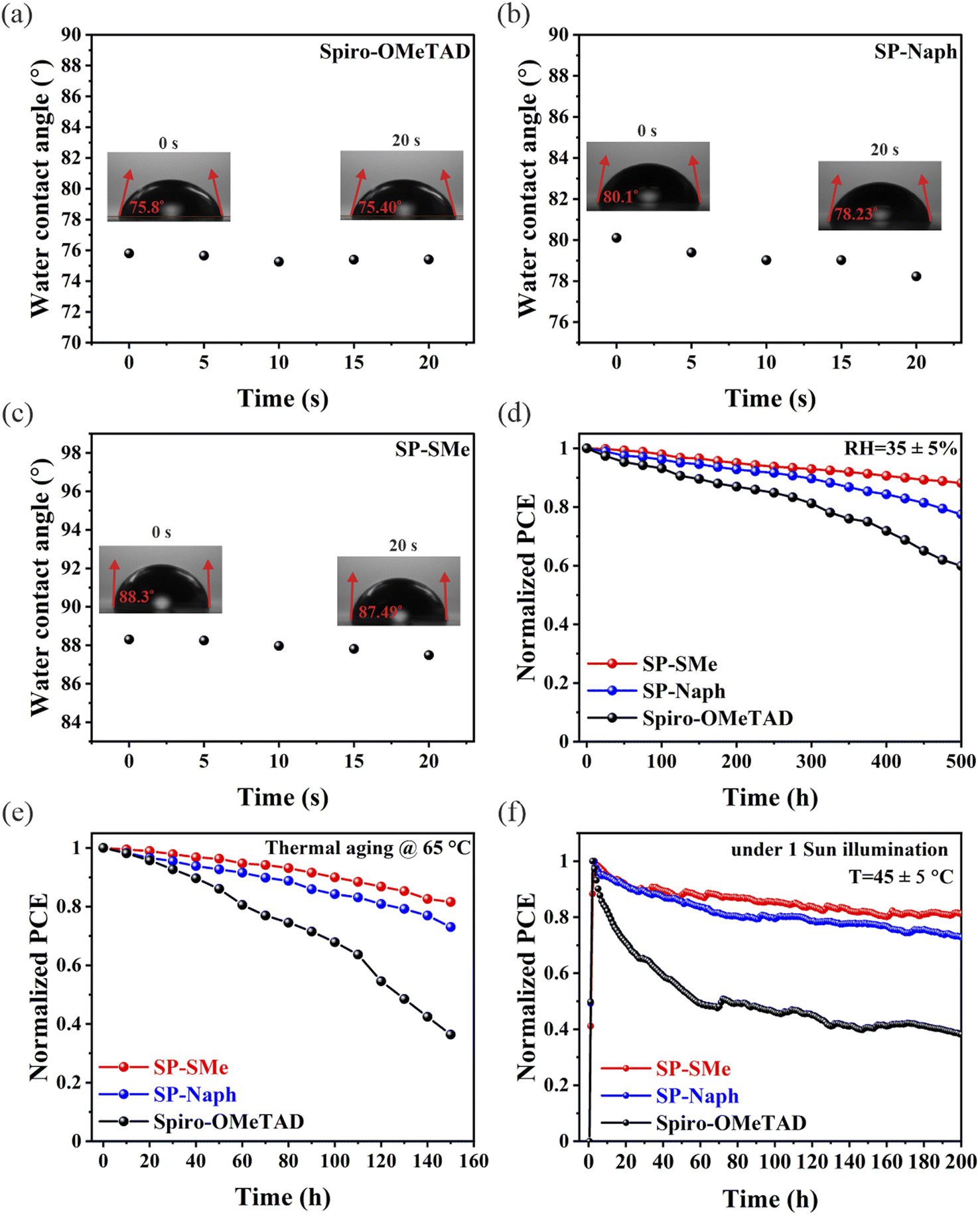 | ||
| Fig. 3 (a–c) Static contact angle measurements of water drop on top of the perovskite/HTL films. (d) Long-term environmental stability test of the unencapsulated devices with different HTMs under ambient conditions with a relative humidity of 35 ± 5%. (e) Thermal stability test of the devices with different HTMs at 65 °C under an inert atmosphere. (f) Operational stability of the devices with different HTMs under MPP tracking with continuous 1 sun illumination in a N2 atmosphere at 45 ± 5 °C. | ||
3 Conclusion
In conclusion, we have designed new cost-effective molecules based on the SFX-core (SP-Naph and SP-SMe), which can be easily synthesized and utilized as dopant-free HTMs for high efficiency and stable PSCs. The structure–property relationship of these HTMs was thoroughly investigated by combining experimental and simulation methods. The influence of SP-Naph and SP-SMe on the photovoltaic performance was compared with the devices based on the benchmark spiro-OMeTAD HTM. It was found that the performance of devices with SP-SMe exceeds that of devices based on SP-Naph-based and doped spiro-OMeTAD. In addition, the SP-SMe-based PSC exhibited superior ambient, thermal and operational stabilities compared with the SP-Naph and spiro-OMeTAD-based devices. These results are attributed to the beneficial properties of the SP-SMe HTM such as its deeper-lying HOMO, higher thermal decomposition temperature and higher hydrophobicity compared to other investigated HTMs. Furthermore, the favorable band energy alignment of SP-SMe with the perovskite layer and its stronger interaction with the undercoordinated Pb2+ in the perovskite film facilitate the charge transfer and reduce non-radiative recombination at the perovskite/HTL interface. This study suggests that the modification of diphenylamine motifs with functional groups (SP-SMe) rather than the extension of the π conjugated aromatic structure (SP-Naph) is a promising direction to achieve stable and efficient PSCs.4 Experimental section
4.1 Materials
All chemicals and solvents were used without any further purification unless stated. Solvents were bought from Chempure (Poland). Lead iodide (PbI2, 99.9985%, trace metal basis), lead bromide (PbBr2) (98%), spiro-OMeTAD (99%), bis(trifluoromethane)sulfonimide lithium salt (LiTFSI) (99.95%), 4-tert-butylpyridine (tBP), N,N-dimethylformamide (DMF) (anhydrous, 99.8%), dimethyl sulfoxide (DMSO) (anhydrous, 99.8%), chlorobenzene (CB) (anhydrous, 99.8%), and acetonitrile (anhydrous, 99.8%) were purchased from Sigma-Aldrich. Formamidinium iodide (FAI) (>99.99%), methylammonium bromide (MABr) (>99.99%), and FK 209 Co(III)TFSI (98%) were purchased from Greatcell Solar Ltd. Tin(IV) oxide (SnO2) aqueous colloidal solution (15% in H2O colloidal dispersion), which contains SnO2 colloidal particles was purchased from Alfa Aesar.4.2 Device fabrication
Indium tin oxide (ITO) glass substrates were cleaned with Hellmanex, water, ethanol, acetone, and isopropyl alcohol for 20 min, respectively, and treated for 20 min with ultraviolet ozone. After that, a compact SnO2 layer of thickness about 20–30 nm was deposited on the surface of ITO by spin coating at 4000 rpm for 30 s and annealed for 30 min at 150 °C. A triple cation perovskite solution having the composition of [Cs0.05(FA0.95MA0.05)0.95Pb(I0.95Br0.05)3] was prepared with CsI (50 μL from 1.5 M stock solution in DMSO), FAI (0.172 g), MABr (0.022 g), PbI2 (0.508 g), PbBr2 (0.807 g), and DMSO:DMF = 400 μL:600 μL. The solution of perovskite was spin-coated at 1000 rpm for 10 s and then at 6000 rpm for 30 s. During the second step, chlorobenzene as antisolvent was poured on the spinning perovskite surface 15 s prior to the end of time. Then, all substrates were transferred to the hot plate immediately and annealed at 100 °C for one hour. Subsequently, hole transport layer (HTL) solution (70 mM spiro-OMeTAD in 1 mL of chlorobenzene including 36 μL of tBP and 18 μL of Li-TFSI solution (520 mg Li-TFSI in 1 mL acetonitrile)) and the HTLs (SP-SMe and SP-Naph) was spin-coated at 4000 rpm for 20 s. Finally, 80 nm of the gold electrode was deposited with a thermal evaporator.
| Eads = Eslab_mol − Eslab − Emol |
| HOMO (eV) = −4.8 − (Eonset.oxi − E1/2 (ferrocene)) |
| LUMO (eV) = −4.8 − (Eonset.red − E1/2 (ferrocene)) |
Author contributions
S. P. S. and D. P. conceived the idea. V. K., D. K., K. P. K. and B. Y. synthesized and characterized the hole transporting materials. R. D. C. fabricated the films and devices and performed various characterization studies. M. A. did the theoretical calculation. J. K. performed conductivity and contact angle measurements. A. M. conducted and analyzed EIS measurements. J. N. performed SEM measurements. K. N. conducted XPS measurements. N. M. and P. S. performed TRPL and GIWAXS measurements. S. A. performed AFM. P. Y., S. A., S. P. S. and D. P. analyzed all the data. R. D. C. and D. P. wrote the manuscript. D. P. directed and supervised this project. All authors discussed the results and commented on the manuscript.Conflicts of interest
There are no conflicts to declare.Acknowledgements
V. K. thanks UGC for providing a Senior Research Fellowship and D. K. is thankful to DST for providing Inspire Fellowship. K. P. K. is thankful to CSIR for providing Senior Research Fellowship. S. P. S. acknowledges financial support from DST (DST/INT/ISR-P-27/2020) and CSIR-IICT Communication Number: IICT/Pubs./2024/071. R. D. C., M. A., J. K., and D. P. acknowledge the National Science Centre (grant SONATA BIS 10, no. 2020/38/E/ST5/00267) for financial support. N. M. and P. S. acknowledge the support of the Slovak Research and Development Agency (SK-CZ-RD-21-0043 and APVV-21-0297), the Slovak Academy of Sciences (SAS-MOST/JRP/2021/192/Pb-free-PSC) and ITMS project code 313021T081. The computational study was carried out with the support of the Interdisciplinary Centre for Mathematical and Computational Modelling at the University of Warsaw (ICM UW) under computational allocation no. g94-1719.References
- Best Research-Cell Efficiency Chart, https://www.nrel.gov/pv/cellefficiency.html, accessed September 2023 Search PubMed.
- C. C. Boyd, R. Cheacharoen, T. Leijtens and M. D. McGehee, Chem. Rev., 2019, 119, 3418–3451 CrossRef CAS.
- R. Wang, M. Mujahid, Y. Duan, Z. Wang, J. Xue and Y. Yang, Adv. Funct. Mater., 2019, 29, 1808843 CrossRef CAS.
- Z. Zhao, F. Gu, H. Rao, S. Ye, Z. Liu, Z. Bian and C. Huang, Adv. Energy Mater., 2019, 9, 1802671 CrossRef.
- Z. Song, A. Abate, S. C. Watthage, G. K. Liyanage, A. B. Phillips, U. Steiner, M. Graetzel and M. J. Heben, Adv. Energy Mater., 2016, 6, 1600846 CrossRef.
- Y.-B. Lu, W.-Y. Cong, C. Guan, H. Sun, Y. Xin, K. Wang and S. Song, J. Mater. Chem. A, 2019, 7, 27469–27474 RSC.
- D. Bryant, N. Aristidou, S. Pont, I. Sanchez-Molina, T. Chotchunangatchaval, S. Wheeler, J. R. Durrant and S. A. Haque, Energy Environ. Sci., 2016, 9, 1655–1660 RSC.
- E. J. Juarez-Perez, Z. Hawash, S. R. Raga, L. K. Ono and Y. Qi, Energy Environ. Sci., 2016, 9, 3406–3410 RSC.
- J. Song, H. Liu, W. Pu, Y. Lu, Z. Si, Z. Zhang, Y. Ge, N. Li, H. Zhou, W. Xiao, L. Wang and M. Sui, Energy Environ. Sci., 2022, 15, 4836–4849 RSC.
- S.-W. Lee, S. Kim, S. Bae, K. Cho, T. Chung, L. E. Mundt, S. Lee, S. Park, H. Park, M. C. Schubert, S. W. Glunz, Y. Ko, Y. Jun, Y. Kang, H.-S. Lee and D. Kim, Sci. Rep., 2016, 6, 38150 CrossRef CAS.
- Y. Cheng and L. Ding, Energy Environ. Sci., 2021, 14, 3233–3255 RSC.
- S. P. Dunfield, L. Bliss, F. Zhang, J. M. Luther, K. Zhu, M. F. A. M. Van Hest, M. O. Reese and J. J. Berry, Adv. Energy Mater., 2020, 10, 1904054 CrossRef CAS.
- A. Mahapatra, D. Prochowicz, M. M. Tavakoli, S. Trivedi, P. Kumar and P. Yadav, J. Mater. Chem. A, 2020, 8, 27–54 RSC.
- S. Akin, N. Arora, S. M. Zakeeruddin, M. Grätzel, R. H. Friend and M. I. Dar, Adv. Energy Mater., 2020, 10, 1903090 CrossRef CAS.
- A. R. B. Mohd Yusoff, M. Vasilopoulou, D. G. Georgiadou, L. C. Palilis, A. Abate and M. K. Nazeeruddin, Energy Environ. Sci., 2021, 14, 2906–2953 RSC.
- D. Prochowicz, R. Runjhun, M. M. Tavakoli, P. Yadav, M. Saski, A. Q. Alanazi, D. J. Kubicki, Z. Kaszkur, S. M. Zakeeruddin, J. Lewiński and M. Grätzel, Chem. Mater., 2019, 31, 1620–1627 CrossRef CAS.
- M. T. Mbumba, D. M. Malouangou, J. M. Tsiba, M. W. Akram, L. Bai, Y. Yang and M. Guli, J. Mater. Chem. C, 2021, 9, 14047–14064 RSC.
- J. Wang, G. Jin, Q. Zhen, C. He and Y. Duan, Adv. Mater. Interfaces, 2021, 8, 2002078 CrossRef CAS.
- W. Zhao, J. Xu, K. He, Y. Cai, Y. Han, S. Yang, S. Zhan, D. Wang, Z. Liu and S. Liu, Nano-Micro Lett., 2021, 13, 169 CrossRef CAS.
- R. Wang, A. Altujjar, N. Zibouche, X. Wang, B. F. Spencer, Z. Jia, A. G. Thomas, M. Z. Mokhtar, R. Cai, S. J. Haigh, J. M. Saunders, M. S. Islam and B. R. Saunders, Energy Environ. Sci., 2023, 16, 2646–2657 RSC.
- V. Manjunath, S. Bimli, P. A. Shaikh, S. B. Ogale and R. S. Devan, J. Mater. Chem. C, 2022, 10, 15725–15780 RSC.
- Y. Zhu, K. Deng, H. Sun, B. Gu, H. Lu, F. Cao, J. Xiong and L. Li, Adv. Sci., 2018, 5, 1700614 CrossRef.
- Y. Ma, K. Deng, B. Gu, F. Cao, H. Lu, Y. Zhang and L. Li, Adv. Mater. Interfaces, 2016, 3, 1600729 CrossRef.
- D. Liu, S. Li, P. Zhang, Y. Wang, R. Zhang, H. Sarvari, F. Wang, J. Wu, Z. Wang and Z. D. Chen, Nano Energy, 2017, 31, 462–468 CrossRef CAS.
- R. D. Chavan, M. M. Tavakoli, D. Prochowicz, P. Yadav, S. S. Lote, S. P. Bhoite, A. Nimbalkar and C. K. Hong, ACS Appl. Mater. Interfaces, 2020, 12, 8098–8106 CrossRef CAS PubMed.
- H. Min, D. Y. Lee, J. Kim, G. Kim, K. S. Lee, J. Kim, M. J. Paik, Y. K. Kim, K. S. Kim, M. G. Kim, T. J. Shin and S. Il Seok, Nature, 2021, 598, 444–450 CrossRef CAS PubMed.
- M. Kim, J. Jeong, H. Lu, T. K. Lee, F. T. Eickemeyer, Y. Liu, I. W. Choi, S. J. Choi, Y. Jo, H.-B. Kim, S.-I. Mo, Y.-K. Kim, H. Lee, N. G. An, S. Cho, W. R. Tress, S. M. Zakeeruddin, A. Hagfeldt, J. Y. Kim, M. Grätzel and D. S. Kim, Science, 2022, 375, 302–306 CrossRef CAS PubMed.
- R. D. Chavan, M. Wolska-Pietkiewicz, D. Prochowicz, M. Jędrzejewska, M. M. Tavakoli, P. Yadav, C. K. Hong and J. Lewiński, Adv. Funct. Mater., 2022, 32, 2205909 CrossRef CAS.
- J. H. Lee, S. Lee, T. Kim, H. Ahn, G. Y. Jang, K. H. Kim, Y. J. Cho, K. Zhang, J.-S. Park and J. H. Park, Joule, 2023, 7, 380–397 CrossRef CAS.
- L. Yang, H. Zhou, Y. Duan, M. Wu, K. He, Y. Li, D. Xu, H. Zou, S. Yang, Z. Fang, S. Liu and Z. Liu, Adv. Mater., 2023, 35, 2211545 CrossRef CAS PubMed.
- Z. Dai, S. K. Yadavalli, M. Chen, A. Abbaspourtamijani, Y. Qi and N. P. Padture, Science, 2021, 372, 618–622 CrossRef CAS PubMed.
- J. Kruszyńska, J. Ostapko, V. Ozkaya, B. Surucu, O. Szawcow, K. Nikiforow, M. Hołdyński, M. M. Tavakoli, P. Yadav, M. Kot, G. P. Kołodziej, M. Wlazło, S. Satapathi, S. Akin and D. Prochowicz, Adv. Mater. Interfaces, 2022, 9, 2200575 CrossRef.
- X. Xin, J. Yang, X. Pu, Y. Li, T. Wang, H. Chen, Q. Cao, Y. Zhang, I. Tojiboyev, H. Salari, F. Ye and X. Li, Adv. Mater. Interfaces, 2022, 9, 2200102 CrossRef CAS.
- R. D. Chavan, B. Bończak, J. Kruszyńska, A. Mahapatra, M. Ans, J. Nawrocki, K. Nikiforow, P. Yadav, J. Paczesny, F. Sadegh, M. Unal, S. Akin and D. Prochowicz, Chem. Mater., 2023, 35, 8309–8320 CrossRef CAS.
- F. M. Rombach, S. A. Haque and T. J. Macdonald, Energy Environ. Sci., 2021, 14, 5161–5190 RSC.
- G. Tumen-Ulzii, C. Qin, T. Matsushima, M. R. Leyden, U. Balijipalli, D. Klotz and C. Adachi, Sol. RRL, 2020, 2000305 CrossRef CAS.
- H. D. Pham, T. C. Yang, S. M. Jain, G. J. Wilson and P. Sonar, Adv. Energy Mater., 2020, 10, 1903326 CrossRef CAS.
- H. D. Pham, S. M. Jain, M. Li, Z. Wang, S. Manzhos, K. Feron, S. Pitchaimuthu, Z. Liu, N. Motta, J. R. Durrant and P. Sonar, Adv. Electrode Mater., 2020, 6, 1900884 CrossRef CAS.
- K. Kranthiraja, R. Nishikubo and A. Saeki, Energy Adv., 2023, 2, 1030–1035 RSC.
- A. K. Jena, M. Ikegami and T. Miyasaka, ACS Energy Lett., 2017, 2, 1760–1761 CrossRef CAS.
- E. J. Juarez-Perez, M. R. Leyden, S. Wang, L. K. Ono, Z. Hawash and Y. Qi, Chem. Mater., 2016, 28, 5702–5709 CrossRef CAS.
- N. J. Jeon, H. G. Lee, Y. C. Kim, J. Seo, J. H. Noh, J. Lee and S. I. Seok, J. Am. Chem. Soc., 2014, 136, 7837–7840 CrossRef CAS PubMed.
- Z. Hu, W. Fu, L. Yan, J. Miao, H. Yu, Y. He, O. Goto, H. Meng, H. Chen and W. Huang, Chem. Sci., 2016, 7, 5007–5012 RSC.
- B. Xu, D. Bi, Y. Hua, P. Liu, M. Cheng, M. Grätzel, L. Kloo, A. Hagfeldt and L. Sun, Energy Environ. Sci., 2016, 9, 873–877 RSC.
- M. Maciejczyk, A. Ivaturi and N. Robertson, J. Mater. Chem. A, 2016, 4, 4855–4863 RSC.
- D. Bi, B. Xu, P. Gao, L. Sun, M. Grätzel and A. Hagfeldt, Nano Energy, 2016, 23, 138–144 CrossRef CAS.
- B. Xu, J. Zhang, Y. Hua, P. Liu, L. Wang, C. Ruan, Y. Li, G. Boschloo, E. M. J. Johansson, L. Kloo, A. Hagfeldt, A. K.-Y. Jen and L. Sun, Chem, 2017, 2, 676–687 CAS.
- V. A. Chiykowski, Y. Cao, H. Tan, D. P. Tabor, E. H. Sargent, A. Aspuru-Guzik and C. P. Berlinguette, Angew. Chem., Int. Ed., 2018, 57, 15529–15533 CrossRef CAS.
- H. J. Snaith and M. Grätzel, Appl. Phys. Lett., 2006, 89, 262114 CrossRef.
- M. Jeong, I. W. Choi, K. Yim, S. Jeong, M. Kim, S. J. Choi, Y. Cho, J.-H. An, H.-B. Kim, Y. Jo, S.-H. Kang, J.-H. Bae, C.-W. Lee, D. S. Kim and C. Yang, Nat. Photonics, 2022, 16, 119–125 CrossRef CAS.
- Q. Sun, J. Zhang, Q. Chen, Y. Wang, Y. Zhou, B. Song, X. Jia, N. Yuan, J. Ding and Y. Li, J. Power Sources, 2020, 449, 227488 CrossRef CAS.
- H. Guo, H. Zhang, C. Shen, D. Zhang, S. Liu, Y. Wu and W. Zhu, Angew. Chem., Int. Ed., 2021, 60, 2674–2679 CrossRef CAS.
- J.-W. Lee, S.-H. Bae, Y.-T. Hsieh, N. De Marco, M. Wang, P. Sun and Y. Yang, Chem, 2017, 3, 290–302 CAS.
- P. Yadav, D. Prochowicz, M. Saliba, P. Boix, S. Zakeeruddin and M. Grätzel, Crystals, 2017, 7, 252 CrossRef.
- G. Zhu, L. Yang, C. Zhang, G. Du, N. Fan, Z. Luo, X. Zhang and J. Zhang, ACS Appl. Energy Mater., 2022, 5, 3595–3604 CrossRef CAS.
- T. Malinauskas, D. Tomkute-Luksiene, R. Sens, M. Daskeviciene, R. Send, H. Wonneberger, V. Jankauskas, I. Bruder and V. Getautis, ACS Appl. Mater. Interfaces, 2015, 7, 11107–11116 CrossRef CAS.
- T. Lu and F. Chen, J. Comput. Chem., 2012, 33, 580–592 CrossRef CAS.
- M. D. Hanwell, D. E. Curtis, D. C. Lonie, T. Vandermeersch, E. Zurek and G. R. Hutchison, J. Cheminf., 2012, 4, 17 CAS.
- G. Kresse and D. Joubert, Phys. Rev. B: Condens. Matter Mater. Phys., 1999, 59, 1758–1775 CrossRef CAS.
- J. P. Perdew, K. Burke and M. Ernzerhof, Phys. Rev. Lett., 1996, 77, 3865–3868 CrossRef CAS.
- L. Fu, H. Li, L. Wang, R. Yin, B. Li and L. Yin, Energy Environ. Sci., 2020, 13, 4017–4056 RSC.
- K. Momma and F. Izumi, J. Appl. Crystallogr., 2011, 44, 1272–1276 CrossRef CAS.
Footnotes |
| † Electronic supplementary information (ESI) available. See DOI: https://doi.org/10.1039/d3ta07851e |
| ‡ These authors contributed equally to this work. |
| § Current address: Light Technology Institute, Karlsruhe Institute of Technology (KIT), Engesserstraße 13, 76131 Karlsruhe, Germany. |
| This journal is © The Royal Society of Chemistry 2024 |