
 Open Access Article
 This Open Access Article is licensed under a
 Creative Commons Attribution 3.0 Unported Licence
Recyclable in-mold and printed electronics with polymer separation layers†
Yannic
Brasse
 a,
Mariano
Laguna Moreno
a,
Simon
Blum
a,
Tim
Horter
b,
Florian
Janek
b,
Kerstin
Gläser
b,
Carl
Emmerechts
c,
Jean-Michel
Clanet
d,
Michèle
Verhaert
d,
Benoît
Grymonprez
d and
Tobias
Kraus
*ae
a,
Mariano
Laguna Moreno
a,
Simon
Blum
a,
Tim
Horter
b,
Florian
Janek
b,
Kerstin
Gläser
b,
Carl
Emmerechts
c,
Jean-Michel
Clanet
d,
Michèle
Verhaert
d,
Benoît
Grymonprez
d and
Tobias
Kraus
*ae
aINM – Leibniz Institute for New Materials, Structure Formation Group, Campus D2 2, 66123 Saarbrücken, Germany. E-mail: tobias.kraus@leibniz-inm.de
bHahn-Schickard-Gesellschaft für angewandte Forschung, Allmandring 9b, 70569 Stuttgart, Germany
cSirris, Liège Science Park, Rue Bois Saint-Jean 12, 4102 Seraing, Belgium
dCTP Centre Terre et Pierre, Chau. d'Antoing 55, 7500 Tournai, Belgium
eSaarland University, Colloid and Interface Chemistry, Campus D2 2, 66123 Saarbrücken, Germany
First published on 16th May 2024
Abstract
Recycling of Waste from Electrical and Electronic Equipment (WEEE) is crucial in preventing resource depletion and promoting a circular economy. The increasing fraction of printed and in-mold electronics is particularly challenging. The combinations of polymers and printed metals are difficult to disassemble due to the strong interfaces that are formed to create reliable in-mold devices. The relatively low metal content makes recycling uneconomical and those valuable materials are then lost to landfill or incineration. Separation layers enable design-for-recycling with minimal modifications during the fabrication process, while preserving product performance and reliability. We present a scalable method for preparing polymer separation layers for printed and in-mold electronics. Slot-die coating is used to prepare water-soluble polymer films with a dry thickness of less than 10 μm on commodity polymer substrates. This separation layer improves the bending stability of inkjet- and screen-printed circuits. Furthermore, it is compatible with typical polymer processing methods, such as thermoforming and injection molding. Various methods, including plasma treatment, are presented to ensure adhesion of the modified interfaces. Finally, we investigate the material recovery and demonstrate the release of the integrated metal within a few minutes by dissolving the separation layer in water. This material recovery process can be readily integrated into current WEEE recycling processes.
Sustainability spotlightPrecious metals and conventional polymers, based on non-renewable resources, are used in most electronic devices as conductive and insulating parts. Therefore, the management of Waste from Electrical and Electronic Equipment (WEEE) in the context of a circular economy is essential. Recycling of polymer-embedded (in-mold) electronics is currently inefficient due to the strong connection between metals and polymers. This makes their recovery uneconomical as recycling is not considered in the design of such products. Here, we introduce a design-for-recycling approach that enables a more efficient recovery of the components with existing recycling processes. We are targeting the action network ‘Green economy’ as part of the UN Sustainable Development Goal ‘Decent work and economic growth’ (SDG 8). The approach also addresses the goals ‘Industry, innovation and infrastructure (SDG 9) and ‘Responsible consumption and production’ (SDG 12). |
Introduction
Printed electronics are the centerpiece of an exponentially growing market with applications in logistics,1 internet of things (IoT) devices,2 and flexible sensors.3 They can replace printed circuit boards (PCBs) in low-performance applications,4 providing a more sustainable alternative.5 However, economic and ecologic benefits of printed electronics are no intrinsic advantages of the technology but need to be considered in the design of products.4 These may be achieved by lightweight construction using in-mold electronics (IME), use of sustainable substrate materials such as paper or biopolymers, or consideration of recyclability and reusability of the individual components. A major challenge in making printed electronics more eco-friendly is that they are composite materials that require high energy input for their recycling. Although there are well-established routes for collecting Waste from Electrical and Electronic Equipment (WEEE) in the European Union and elsewhere, inseparable composite parts are often incinerated, after which the metallic fractions are recovered.6,7 Due to their low metal content and high combustibility, this process is particularly relevant for printed electronics.8 These are commonly based on conductive silver tracks produced by contact methods (e.g. screen printing and gravure printing) or non-contact methods (e.g. inkjet printing and aerosol printing).9 There are alternatives such as tracks made from copper, conductive polymers, or carbon-based materials,10 but silver is the most abundant due to its high conductivity, sufficient oxidation stability and good processability.11,12 The most common substrates for printing are paper-based materials or polymers such as polyethylene terephthalate (PET), polyethylene naphthalate (PEN) and polycarbonate (PC) due to their low cost and excellent processability.10 The advantage of using polymers is their compatibility with further processing steps, such as thermoforming and overmolding, which are used with PC to create IME.Approaches to improve the sustainability of printed electronics in literature focus on the recovery of valuable silver.13 A straightforward solution is to replace the substrate material with water-soluble alternatives such as polyvinyl alcohol (PVA).14 Although this allows for direct release of the silver, it is limited to specialized applications due to the mechanical properties of PVA and its susceptibility to water. Recent approaches utilized degradable materials such as polycaprolactone or polylactic acid for the recycling.15,16 Jaiswal et al. studied cellulose nanocomposites as compostable substrates for flexible electronics.17 Degradation in soil for 3 weeks was sufficient to separate their electronic components and recover them via sieving. These approaches have potential, but will not be immediately economically viable because biodegradation is hardly compatible with the current electronic waste treatment and will require changes to the WEEE directives.4,18
Today, material recovery from WEEE is typically achieved by a series of manual disassembly and presorting, comminution, automated sorting, and finally, hydro- or pyrometallurgical processing.19 Conventional, less integrated electronic waste with PCBs, solder and wiring can be largely separated by shredding and subsequent sorting using density, magnetic, or Eddy current separation.6,19 These methods are inefficient for the separation of integrated materials such as IME due to low metal fractions and their adhesion to the polymer matrix. This results in either loss of the metal or increased amount of polymer impurities in the metallic fraction. Solvent-based methods for depolymerizing or dissolving the matrix materials address this issue and typically yield higher purity materials compared to mechanical recycling.20,21 However, the economic viability of dissolution/precipitation processes is limited by the use of harmful solvents such as dichlormethane (DCM) and the energy consumption for solvent evaporation.22,23 Since this strongly depends on the purity of the waste streams, recent literature promotes the combination of solvent-based and mechanical methods.22,24,25 To facilitate the separation of IME, a straightforward recycling approach that is compatible with the established sorting processes is required.
Here, we report on a “recyclability by design” strategy that requires only limited adaptations in the IME production process and does not affect the performance of the product until the end of its life. We demonstrate the use of a water-soluble release layer to improve sustainability of printed and in-mold electronics. Our process utilizes polyvinyl alcohol (PVA) to coat PC foils that are subsequently printed with conductive silver, thermoformed, and overmolded with PC (see Fig. 1). After grinding, the PVA layer facilitates the separation of silver and polycarbonate by immersion in water and subsequent sieving. We discuss the impact of the separation layer on the material recovery, the processability of printed electronics and the impact on their electromechanical properties.
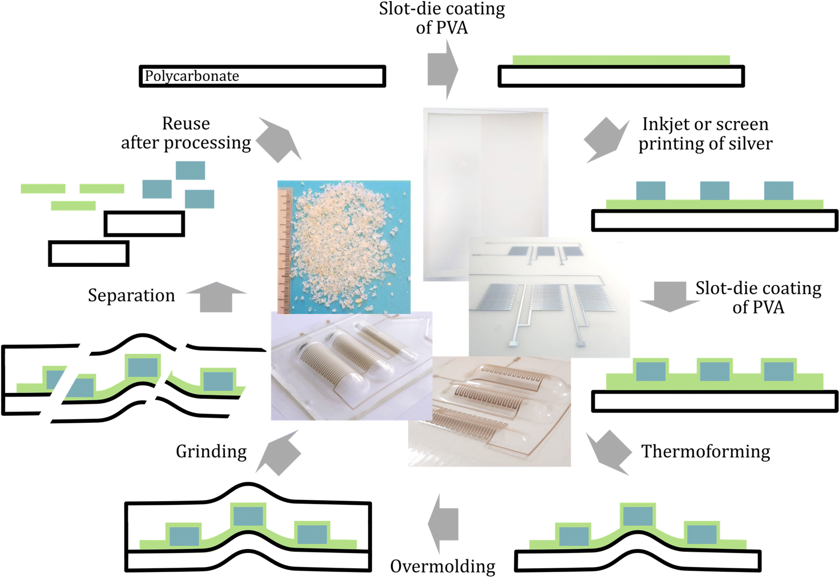 | ||
| Fig. 1 Concept of the design-for-recycling of integrated electronics. Separation layers are introduced prior to printing of conductive tracks. After polymer processing using thermoforming and injection molding, the materials can be separated by dissolution of the PVA separation layer. | ||
Results and discussion
Reliability of printed electronics with separation layers
Introducing a release layer in the fabrication process of printed electronics can change the properties of the printed structures. Mechanical properties of the conductive tracks and their electrical conductivities may change due to shrinkage or diffusion of the separation layer into the metallic layer. To study the influence of the interlayer on these properties, the electric resistivity was measured before and during cyclic bending tests and was compared for samples with and without the separation layer. This test allows conclusions about electrical connection failure due to mechanical stress.A polyvinyl alcohol (PVA) separation layer was prepared by slot-die coating on polycarbonate (PC) foils using aqueous solutions with a polymer mass fraction of 6%. PVA with 88% degree of hydrolysis was applied due to improved cold water solubility compared to fully hydrolyzed alternatives.26 The resulting layer had an area density of 3.2 ± 0.7 g m−2 corresponding to a film thickness of 2.5 ± 0.6 μm. For printing of conductive tracks onto PVA, screen printing (contact method) and inkjet printing (non-contact, drop-on-demand method) were utilized, as these are common techniques that complement each other regarding initial costs, production scale and printing precision.27
Screen printing offers a high layer thickness per transit in the range of few micrometers up to one hundred micrometers, depending on the applied mesh size and paste. It is suitable for medium quantities due to the initial costs of the mask. The viscosity of the paste is typically in the range of 5 × 10² to 103 mPa s.3 Here, two pastes with silver microparticles were applied (Dycotec DM SiP 2002 and Bectron CP 6680). Prints were dried at 130 °C for 30 min in an oven.
Inkjet printing is a digital process without the need for additional masks and is therefore suitable for low quantities, which makes it ideal for prototyping. At less than one micrometer per pass, the thickness of a dried inkjet-printed layer is significantly lower than that of screen-printed structures. The viscosity range for ink jetting is 5–50 mPa s.3 For inkjet printing of tracks on PC and on PVA-coated PC, a commercial ink containing silver nanoparticles was applied (PVNanocell Sicrys I30EG-1). After printing and drying, the ink was sintered at 150 °C for 60 minutes.
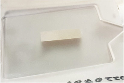
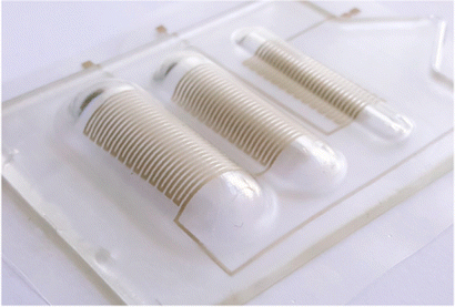
Inkjet- and screen-printed silver tracks on PC sheets are shown in Fig. 2a. The layout was designed to test the reliability of printed silver tracks using 4-wire-measurements to investigate the resistivity change of printed tracks, with and without underlying PVA, during bending tests. The test specimen had a dogbone-shape and a total length of 80 mm. Conductive tracks were printed on the 500 μm PC sheets with and without PVA layer.
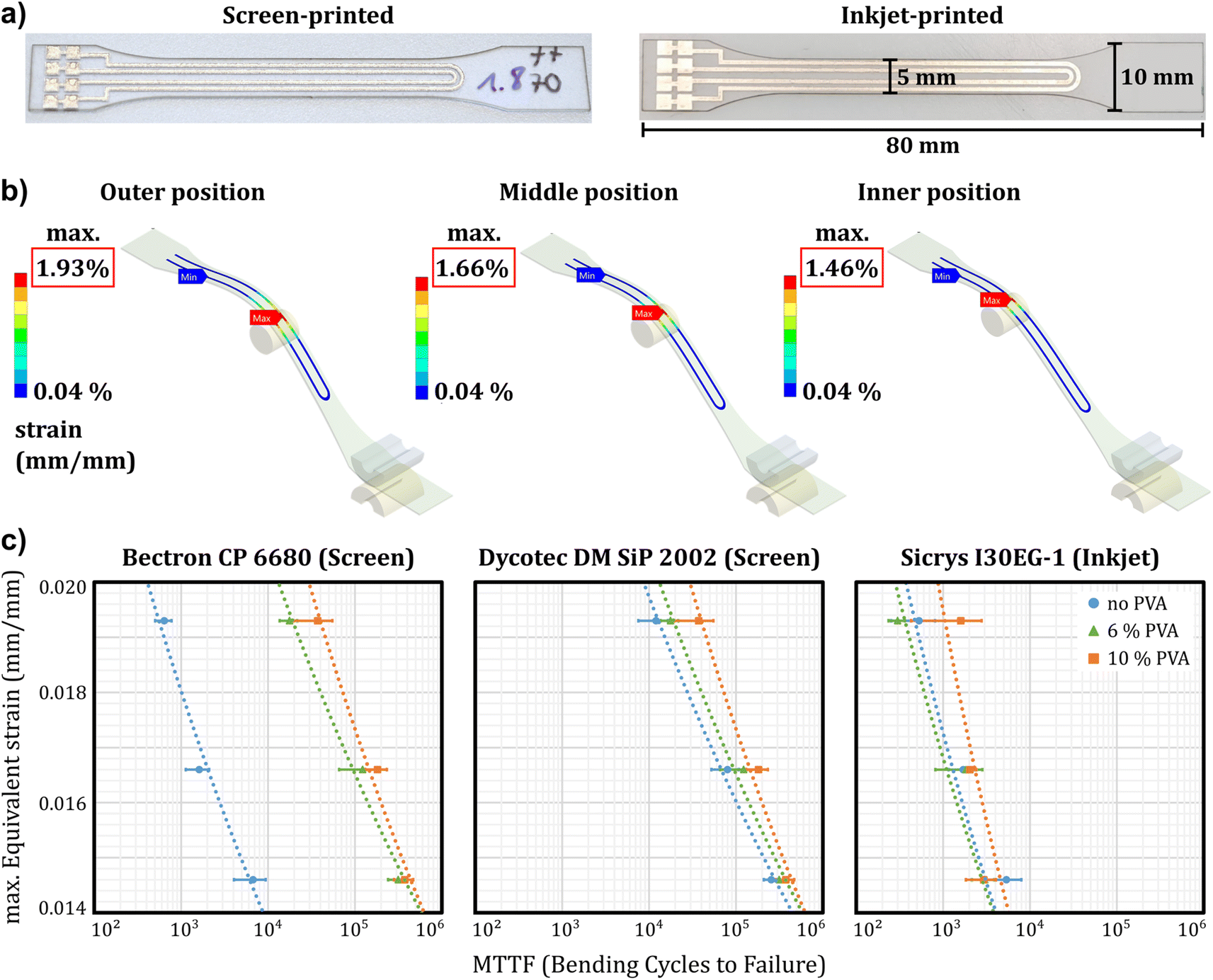 | ||
| Fig. 2 Impact of polyvinyl alcohol (PVA) layers on polycarbonate (PC) on the reliability of printed electronics. (a) Photograph of dogbone-shaped samples with inkjet- and screen-printed silver tracks on laser cut PC sheets (500 μm thickness). (b) Finite element method (FEM) simulation of strain on a bending test rig with a bolt at three different positions, resulting in 1.93% (outer), 1.66% (middle), and 1.46% strain (inner position). (c) Mean time to failure (MTTF)-diagram based on these strains for three different materials: Bectron CP 6680 screen printing paste, Dycotec DM SiP 2002 screen printing paste, and I30-EG01 inkjet ink printed on PC without PVA (blue dots), with PVA layer (green triangles) and with thicker PVA layer (orange squares). | ||
Bending tests were conducted to investigate the influence of an additional separation layer on the reliability of printed electronics by examining the susceptibility of the layer system to crack under cyclic bending loads. The test rig consisted of an electric motor that drives a crankshaft, which causes deflection of a clamped test specimen against a bolt (see ESI 1†). The deflection was set to 24 mm. By adjusting the position of the bolt, it was possible to adjust the strain on the conductive track. Three different positions were chosen for variation of strain on the test specimen, named as inner position, middle position and outer position as indicated in Fig. 2b. The resulting strains generated during the bending test were determined using finite element method (FEM) simulation. The bending conditions are within the typical fracture limits of 1–2% for metal coatings28 and were chosen because they resulted in failure of the printed conductive tracks within a reasonable number of bending cycles. Strains, rather than stresses, were determined due to limited availability of material data for the used silver inks, namely Young's modulus.
A total of eight conductive tracks were tested for each material combination. The resistivity was measured during the cyclic bending load tests. It should be noted that inkjet- and screen-printed conductive tracks showed different initial resistance values. In ESI 1,† exemplary resistance measurements are shown over bending cycles for screen-printed conductors with Dycotec DM SiP 2002 at 1.93% strain. A rapid increase in resistance was observed at the beginning, which transitions into a constant rise for both layer systems, namely with and without underlying PVA layer. The curves' behavior suggests creep processes in the printed conductive tracks during the bending test. Without underlying PVA, a spike of increasing resistance was measured starting around 6 × 10⁴ cycles. This was interpreted as breakage of the conductive track. In comparison, the track with underlying PVA (blue curve) did not show a sharp rise of resistance. It can be concluded that the PVA layer reduces the stresses in the conductive tracks induced by bending, effectively serving as a compensation layer.28
A statistical analysis of failures using Weibull distributions was conducted using the statistical software Minitab® (see ESI 2†). The failure criterion was a 20% increase in resistance from the initial value.29 From the Weibull distributions, the characteristic lifetime was determined, known as Mean Time To Failure (MTTF), which describes the number of cycles until 63.2% of all components have failed. Fig. 2c displays the MTTF-values in dependence of applied strain at the outer position (1.93%), middle position (1.66%), and inner position (1.46%) for the screen-printing paste Dycotec DM SIP 2002, the screen-printing paste Bectron CP 6880, and the inkjet printing ink Sicrys I30-EG1. Two observations can be made from the plots. (i) The reliability of the printed samples decreases with increasing strain. (ii) An underlying PVA-layer leads to an increase of the number of bending cycles until failure. This effect is most pronounced for the screen-printed sample based on the Bectron paste.
To summarize the impact of PVA layers on the mechanical and electrical properties of printed electronics, there is an improvement in the durability of conductive tracks against mechanical stress. This effect is most prominent for screen-printed samples and is likely dependent on the type of solvent used with the ink/paste.
Processability of the separation layer
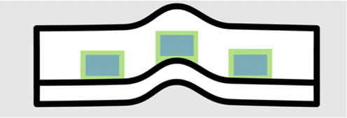
Thermoforming and injection molding are processing steps in the preparation of IME that place additional demands on the properties of our release layer. Therefore, its compatibility with the processing temperatures and its influence on the adhesion between substrate and overmold were studied.10 As substrates, 125 μm PC foils were used for subsequent experiments. Two different geometries of conductive prints were investigated regarding the properties of the conductive tracks and the influence of the separation layer on the processability and recyclability: a simple layout with a 30 × 10 mm2 silver track, here referred as ‘wide tracks’ and a more complex geometry which is referred as ‘meander structure’. The latter comprises a 500 μm wide track that runs through three meander sections that have different radii of curvature after thermoforming. (see Fig. 1 and ESI 3†). Measurement points are located before and after each section to allow the electric resistance measurement for each curvature (2, 4 and 6 mm) as well as the total resistance, which was compared before and after thermoforming (see ESI 4†). The Bectron paste showed the lowest overall resistance, which did not increase significantly after the thermoforming process (3% increase within standard deviation). Therefore, further experiments were conducted using this paste.Printed silver tracks on PVA were overcoated by another PVA layer and subsequently overmolded with 2.5 mm PC. While the samples without PVA layer showed excellent adhesion between the PC foil and the overmold, the PVA-coated samples could be peeled easily. To quantify the adhesion force between PC and PVA, a pull-off test was performed. An adhesive failure between PC and PVA was observed and a tensile strength of 156 ± 15 N cm−2 was determined. Two approaches were tested to improve the adhesion between two polymers: (i) treatment of PC with oxygen plasma and (ii) application of an adhesion-promoting (primer) layer before PVA coating. The first method aims at increasing the hydrophilicity of the PC surface by creating polar species such as hydroxyl, carbonyl and carboxyl groups on the surface, which leads to attractive interactions with the OH-groups of PVA.30,31 The second method utilizes a primer that exhibits strong interactions with both PC and PVA. Here, we used slot-die coated polyvinyl acetate (PVAc) which shows excellent adhesion to PC. Since PVAc is the chemical intermediate in the synthesis of PVA, the same saponification reaction of the acetate group by sodium hydroxide can be used to generate OH-groups on the surface of the primer layer (see Fig. 3a).32 Both methods resulted in an increase of the adhesion that could not be quantified using the pull-off test (see Experimental section for details). Therefore, measurements were performed similar to a standard T-peel test33 as shown in Fig. 3b. To receive symmetrical samples for this test, two PVA-coated sheets were laminated and then peeled. The peel force was measured for PVA on untreated PC, plasma treated PC and PC with saponified PVAc (see Fig. 3c and ESI 5† for detailed setups). By plasma treatment, there is a 51% increase of the peel force whereby the failure is still adhesive between PC and PVA. This situation changes for PC samples with saponified PVAc, where both cohesive failure (rupture of the PVA layer) and adhesive failure between PVA and PVAc could be observed. This is accompanied by a 97% increase of the peel force. The control with the PVAc only (without PVA) revealed that PVAc could not be laminated at 180 °C.
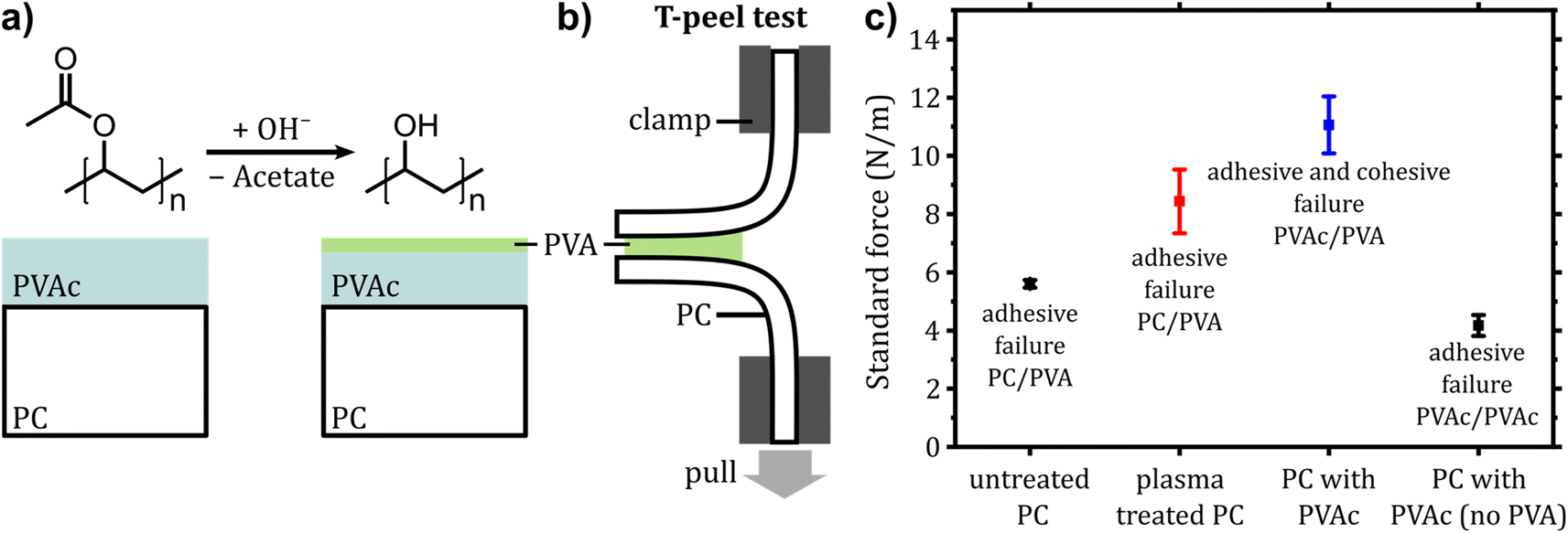 | ||
| Fig. 3 Influence of the PVA layer on the adhesive properties of PC laminates. (a) Schematic of hydrolyzing the surface of a printed PVAc layer. (b) Schematic of a T-peel test using laminated PC foils with PVA. (c) Forces measured in a T-peel test for PVA on differently treated PC layers after lamination (untreated PC, plasma treated PC, PC with saponified PVAc and PC with PVAc but without PVA). | ||
An alternative approach to increasing the adhesion is to reduce the PVA-coated area, which can be achieved by using different slot-die printheads or a different printing technique. This method reduces the use of material significantly and results in the largest possible interfacial area between the PC foil and PC mold, making the influence of the PVA layer on adhesion negligible. Below and above the 30 × 10 mm2 silver tracks, a limited PVA area of 50 × 30 mm2 was applied, which ensures a direct contact between PC foil and 75 × 60 mm2 PC overmold, thus providing good adhesion and protection from humidity. In addition to rectangular coatings under the meander structure, application of PVA patterns by screen and inkjet printing was tested. For inkjet printing, a mixture of dimethyl sulfoxide (DMSO) and water was used to prepare inks, because the high surface tension of pure water prevents droplet formation and its high vapor pressure resulted in clogging of the nozzle. Formulations with a final viscosity of 12–14 mPa s were received using PVA with two different chain lengths (Mw ≈ 31![[thin space (1/6-em)]](https://www.rsc.org/images/entities/char_2009.gif) 000 g mol−1 and Mw ≈ 130000 g mol−1).
000 g mol−1 and Mw ≈ 130000 g mol−1).
The inkjet printing process was strongly influenced by the PVA chain length since only short chain length PVA was printable with the comparable small nozzle sizes of the Samba printhead. For high chain lengths, a rapid clogging of nozzles limited the printability. The wetting behavior on polycarbonate was ideal, therefore no pre-treatment was performed. For screen printing, an optimal viscosity of 2–5 Pa s was obtained using an aqueous solution with the high molecular weight PVA at mass fractions of 13–15%. The printing resulted in pronounced dewetting on PC and formation of bubbles in the PVA layer (see ESI 6†) due to air entrapment during the filling stroke (flooding of the mesh) and lifting of the mesh from the printed paste. To prevent these effects, PC was treated with atmospheric plasma and the surfactant 2,4,7,9-tetramethyl-5-decyne-4,7-diol ethoxylate (TMDD-E) was added to the formulation (10 mmol kg−1). TMDD-E is a non-ionic surfactant that acts both as wetting agent and defoamer by displacing PVA from the air–water interface, which facilitates drainage and bubble coalescence. The resulting prints showed neither bubbles nor dewetting after printing and had an average height of 6 ± 2 μm (see Fig. 4b and c). Subsequently, silver tracks were printed on such PVA layers by screen printing and a second PVA layer was deposited on these tracks. The properties and processibility of these prints regarding thermoforming and injection molding did not differ significantly from silver prints without PVA. The increased contact area between the PC foil and the overmold improves mechanical stability through cohesion and protects the separation layer from humidity, preventing limitations in products that use the separation layer.
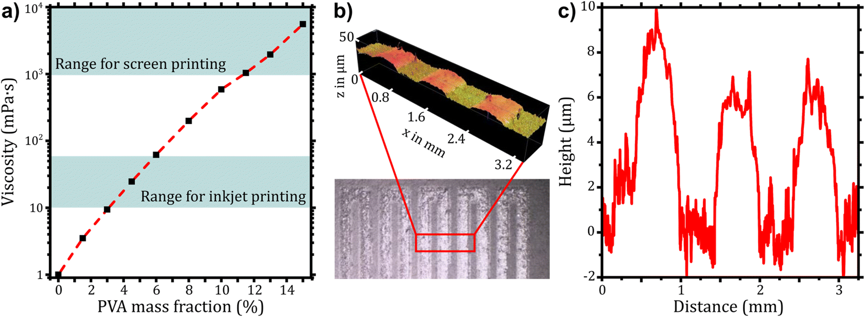 | ||
| Fig. 4 Printing of PVA to prevent reduced adhesion. (a) Viscosity of aqueous solutions with different mass fractions of PVA (130000 g mol−1). (b) Optical microscopy image of PVA on PC and extracted 3D topography from confocal microscopy. (c) Cross section profile over three lines of the meander. | ||
Material separation and recovery
It has been shown that PVA layers improve the reliability of printed electronics and that the impairment of adhesion can be prevented by PC surface treatment or patterned printing of PVA. This final section provides a proof of concept for the integration of this approach into existing recycling processes. The following questions will be addressed: (i) Does the silver detach from the substrates by dissolution of the separation layer? (ii) Is the timeframe reasonable for recycling? (iii) How do parameters such as geometry, temperature and mechanical forces affect the separation process?The separation of the printed silver layer was tested using the wide silver tracks and meander structures before thermoforming/overmolding. Both samples showed separation of the silver layer within 10 min after immersion in water (see Fig. 5a and ESI 7†). This is caused by the high solubility of PVA, its comparably large surface area and low film thickness. The situation changes for overmolded structures where the available surface area for dissolution is limited by the layer thickness and the perimeter of the sample. Overmolded samples with a fully coated PVA layer were kept pendant in water at various temperatures from ambient to 80 °C for 60 minutes. Separation of foil and overmold was not observed for these tests. Therefore, the dissolution of such confined PVA layers was studied in more detail. Laminated PC/PVA/PC samples were cut into squares of either 6 mm or 12 mm side lengths. The polymer release into the aqueous phase under slow stirring was determined using a photometric assay.34 The results are summarized in Fig. 5b. For larger pieces, the released amount of PVA is 2.4 ± 0.5% whereas for smaller pieces the release is about 9.1 ± 0.3% within 8 hours. An increase is expected as the mass transfer rate is proportional to the available area, which grows linearly with decreasing size of the polymer chunks. We attribute the deviation from a proportional behavior to differences in the mixing due to greater movement of the small pieces. This influences the PVA concentration gradient and thus the rate of dissolution. The findings on the dissolution speed of confined PVA suggest that a size reduction of the overmolded samples (initial size of 75 × 60 mm2) is required for industrial recycling.
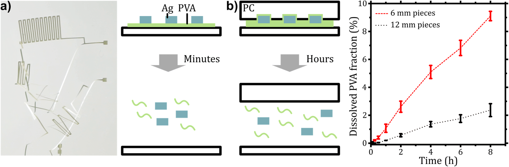 | ||
| Fig. 5 Dissolution of the PVA layer. (a) Photograph and schematic for the release of silver upon contact with water from a fully exposed PVA-coated surface. (b) Schematic of the release for laminated PC/PVA/PC samples and plot of the dissolved PVA fraction versus time in water for 6 mm pieces (dashed red line) and 12 mm pieces (dotted black line). Lines between points are guides for the eye. | ||
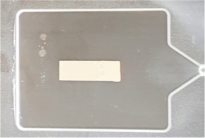
Three different types of overmolded samples (see Table 1) were analyzed for silver recovery using industrial methods: (a) Wide tracks (30 × 10 mm2 silver) with a 50 × 30 mm2 PVA layer below and above silver, (b) Wide tracks without PVA layer, and (c) meander structures with PVA deposited below and above silver by screen printing. A comminution step was required to make the separation layer accessible to water. Knife milling was tested for size reduction but resulted in clogging of the mill. Thus, samples were comminuted with a shredder, which is typically used for recycling of materials such as plastics and wires.35 Shear forces between rotating drums equipped with knifes lead to fragmentation of the samples. A 10 mm calibration grid was used to adjust the size of the milled particles. Beyond size reduction, delamination effects were noticed on the structures. The PC foil and overmold were separated through friction induced by the mills. This delamination was particularly noticeable for sample type (a), which is due to the lowered adhesion in the PVA-coated area.
| (a) Wide track with PVA | (b) Wide track without PVA | (c) Meander with printed PVA | |
|---|---|---|---|
| Schematic |

|
|
|
| Sample appearance |
|
|
|
| Shredding efficiency | Good | Good | Good |
| PC delamination | Yes | Partial | Partial |
| PVA dissolution/silver detachment | Good | None | Partial |
| Density separation | Applicable | Not applicable | Partially applicable |
The dissolution of PVA and the release of silver was tested by immersing shredded samples in water with an agitator at ambient temperature (20 °C) and in hot water (90 °C). In both cases, water dissolved the PVA separation layer on sample type (a) and the ink was released from the PC components within minutes (see Fig. 6). The temperature had a direct effect on the kinetics of the separation. At ambient temperature, the ink separation was achieved in 30 minutes whereas the process was completed in only 5 minutes at 90 °C. The fragments from sample (b) did not undergo further separation of silver and PC due to absence of the release layer. For sample (c) only the delaminated PC pieces were affected by dissolution of PVA, and thus, silver was partially released (see ESI 7†). We conclude that (i) the PVA layer is necessary for proper separation of printed silver and (ii) the layer is required to be in the same size range as the fragmented polymer to ensure delamination of polymer foil and overmold. The delamination occurs either during shredding or by dissolution of the PVA layer under agitation, and is required for the silver release.
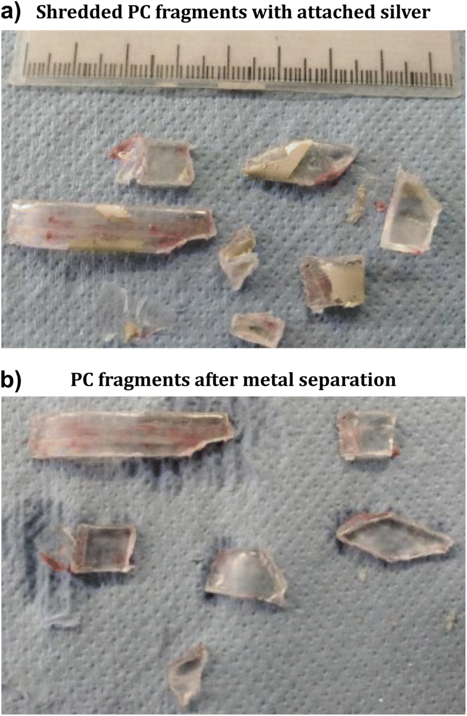 | ||
| Fig. 6 Release of silver from PC by dissolution of the separation layer. (a) Shredded fragments of PC with large silver tracks on PVA layer. (b) Fragments after separation of silver by dissolution of PVA using water at ambient temperature. | ||
The dispersed PC fragments and ink particles from sample (a) were segregated by using a dense medium. Namely, a ZnCl2 solution was adjusted to a specific gravity of 1.3 to make the PC pieces float at the surface (specific gravity of 1.2), whereas the silver ink sedimented. The pieces with ink remaining on the PC, as in samples (b) and (c), also floated because the amount of ink was not sufficient to result in a specific gravity greater than 1.3 (see ESI 8†). A more scalable industrial process for the segregation of PC and ink particles is sieving. Most of the ink particles were recovered as fine particles (<3 mm), while the PC particles were recovered on a 5 mm screen. Some larger ink particles remained with PC particles in the 3–5 mm fraction. An additional breakage step was performed by agitation in an attrition cell to reduce the size of these large ink particles. The dispersion was subjected to high rotation speed for 1 minute and sieved again. Thereafter, the ink particles passed through the 3 mm aperture while the PC particles remained unchanged and were recovered in the oversized fraction (see ESI 8†). Chemical analysis of both fractions revealed that 93.8% of the silver was recovered in the <3 mm fraction, while the residual amount of silver remained in the oversized fraction with the polymer.
Conclusion
The separation of printed conductive tracks from IME was facilitated with PVA interlayers between the polymers and the conductive tracks. Such layers not only maintained the device performance, but even improved the electrical performance of the screen-printed structures under mechanical load by compensating for the stress. Different coating techniques such as slot-die coating, screen printing, and inkjet printing are suitable for PVA deposition, depending on the required geometry. It is necessary for the separation layer to extend beyond the conductive tracks and to be in the same size range as the shredded fragments during the recycling process. This proof-of-concept study shows that up to 94% of the applied silver can be recovered in a separate fraction. We propose that our recovery process can be easily integrated into standard approaches to industrial WEEE recycling as outlined in Fig. 7.6,19 On the industrial scale, dismantling and presorting is typically followed by a size reduction step through shredding. After ferrous metal separation by magnets and non-ferrous metal separation by density or Eddy current, a mixed fraction of light particles is obtained that would require a lot of energy to separate further. Thus, it is usually disposed to landfill or incinerated for waste-to-energy recovery. Our approach utilizes low energy and resource inputs by applying dissolution in water, wet screening and dewatering to recover polymers and printed metals from previously inseparable composites such as IME. The recycling loop can be efficiently closed by smelting of the metal and mechanical recycling or solvent-based purification of the polymer fraction.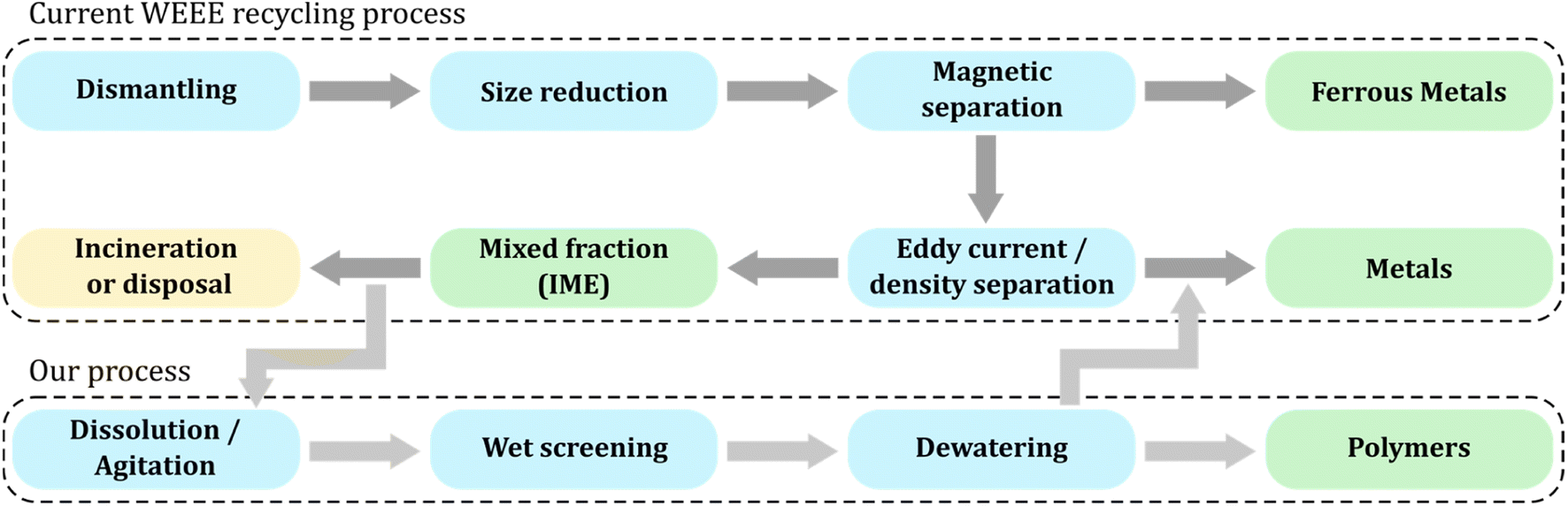 | ||
| Fig. 7 Proposition of a recycling process for Waste from Electrical and Electronic Equipment (WEEE). In the current process, a mixed fraction containing polymers and metallic residues (such as in-mold electronics) is incinerated or disposed because their separation is too energy-intensive. Our process complements the waste treatment to increase recovery of metals and recyclable polymers. Color coding: blue (processing steps), green (recovered materials), yellow (material losses). This figure is based on information from ref. 6 and 19. | ||
Experimental section
Materials
Materials were used as received unless otherwise noted. 125 μm (foil) and 500 μm (sheet) PC Lexan 8B35 matte/velvet (Sabic); Mowiol® 18-88 (Mw ≈ 130000 g mol−1, Sigma-Aldrich); Mowiol® 4-88 (Mw ≈ 31000 g mol−1, Sigma-Aldrich); polyvinyl acetate (Mw ≈ 100000 g mol−1, Sigma-Aldrich); ethanol absolute ≥99.8%, AnalaR NORMAPUR® ACS, Reag. Ph. Eur. analytical reagent (VWR); boric acid, EMPROVE® ESSENTIAL Ph. Eur., BP, JP, NF (Merck); dimethyl sulfoxide (DMSO) ≥99.5%, for synthesis (Roth); iodine-potassium iodide solution acc. to Lugol (Roth); inkjet silver ink TPS303 (Agfa) and Sicrys I30EG-1 (PVNanocell); screen printing silver paste CM 112-15A (Creative Materials), Bectron CP6680 (Elantas), and DM SIP 2002 (Dycotec). Water for ink formulation was purified with a Milli-Q system (Millipore), resulting in a resistivity of 18.2 MΩ cm.
Formulation of PVA
For slot-die coating, solutions of PVA with a mass fraction of 6% (or 10%) were prepared in water. 12 g (or 20 g) Mowiol 18-88 were added to a Schott bottle containing 188 g (or 180 g) of water under vigorous stirring. The addition was made stepwise over two hours to avoid aggregation.For inkjet printing, a solution of PVA with a mass fraction of 3% was prepared in a 9:1 DMSO/water mixture. 180 mL DMSO were added to 20 mL water in a Schott bottle. 90 g of this mixture were added to 10 g of Mowiol 4-88 and stirred for 3 days until a homogeneous stock solution (10%) was yielded. The stock solution was partially diluted to PVA mass fractions of 1–9% with the DMSO/water mixture for viscosity measurements.
For screen printing, solutions of PVA with a mass fraction of 15% were prepared in water. 37.5 g Mowiol 18-88 were added to a Schott bottle containing 212.5 g water at 85% under vigorous stirring. The addition was made stepwise over two hours to avoid aggregation. The mixture was allowed to cool down to room temperature overnight under stirring, yielding a highly viscous solution. It was partially diluted to mass fractions of 1–15% with water for viscosity measurements. 1 g of a 1 mol L−1 solution of 2,4,7,9-tetramethyl-5-decyne-4,7-diol ethoxylate (TMDD-E) was added to the 100 g of the PVA solution and mixed with a speed mixer at 2800 rpm, yielding a 15% Mowiol 18-88 solution with 10 mmol kg−1 TMDD-E.
Rheological characterization of PVA
Rheological characterization was performed using a Modular Compact Rheometer MCR 302e (Anton Paar, Austria). Oscillatory rheology measurements were done at 25 °C with a stainless-steel parallel plate geometry (25 mm) with a gap height of 0.5 mm. The viscosity was determined at different shear rates from 0.1–1000 s−1. A plateau was reached at 10 s−1 for all samples, which was chosen for comparison of the viscosities.Slot-die coating of PVA
Slot-die coating was done with a μPrecision coater (FOM technologies, Denmark). The coating width on A4 size PC Lexan 8B35 foils and sheets was 200 mm at a speed of 0.1 m min−1 and a pump rate of 1.5 mL min−1, resulting in a theoretical wet film thickness of 75 μm. The theoretical layer thickness is 3.5 μm after drying of 6% PVA (density of 1.27 g cm−3). Deviations are considered due to comparably short coating distances which required 20 s precoat pumping and pressure loss in the syringe pump system. As the average surface roughness of the applied PC sheets is Ra ≈ 1 μm, the experimental layer thickness could not be measured with topographical methods such as profilometry or confocal microscopy. It was determined from the amount of PVA deposited on PC using a colorimetric approach (see below). The results were averaged for three A4 sheets with five positions measured each. The determined area density is 3.2 ± 0.7 g m−2, corresponding to a calculated film thickness of 2.5 ± 0.6 μm.Adhesion improvement and lamination
Low pressure oxygen plasma treatment of 10 × 5 cm2 PC foils was conducted in a PlasmaFlecto 30 plasma generator (plasma technology GmbH) for 10 min at 200 W and 0.2 mbar. An oxygen concentrator (5 Liter, DeVilbiss) was used for the gas feed. The chamber was flushed with oxygen for at least 5 min before starting the plasma treatment. PVA coating was done within max. 5 min after the plasma treatment.For preparation of a primer layer, 40 g PVAc were dissolved in 160 g of an ethanol/water mixture (94% mass fraction of ethanol) by stirring for 72 h. The solution was diluted to a PVAc mass fraction of 17%. Slot-die coating was done on 10 × 5 cm2 PC foils using a coating width of 30 mm at a speed of 0.2 m min−1 and a pump rate of 0.6 mL min−1, resulting in a theoretical wet film thickness of 100 μm. The theoretical layer thickness is 14.4 μm after drying of PVAc (density of 1.18 g cm−3).
Plasma-treated, PVAc-coated, and untreated PC foils were slot-die coated with 6% PVA using a coating width of 30 mm at a speed of 0.2 m min−1 and a pump rate of 0.6 mL min−1, resulting in a theoretical wet film thickness of 100 μm. The theoretical layer thickness is 4.7 μm after drying of 6% PVA (density of 1.27 g cm−3).
Lamination of samples (two of each type, receiving a PC/PVA/PC sandwich) was conducted with the universal testing machine Zwick (ZwickRoell) equipped with an oven and ceramic heaters. The oven was pre-heated to 100 °C overnight and the heaters were set to 180 °C. Lamination was achieved by pressing the samples between two 10 × 10 cm2 ceramic heaters. The process comprised a 30 s settling phase at 5 N cm−2, a 15 s unloading phase at 1 N cm−2 and a 300 s loading phase at 100 N cm−1.
Adhesion testing
Two different adhesion tests were performed using the universal testing machine Zwick 1446 (ZwickRoell). The adhesive tensile strength was determined using a 2 × 2 cm2 stainless steel stamp which was attached to the PC backside of laminated samples (cut to 2 × 2 cm2) using double sided adhesive tape (tesa® Doppelseitiges Klebeband 05696 extra stark). Samples were fixated between the stamp and another steel plate with adhesive tape by compression for 3.5 min at 200 N cm−2. The force was then measured at a separation rate of 10 mm min−1. The maximum force was normalized by the area of the stamp and found to be 156 ± 15 N cm−2 for the laminated PVA coated samples (average over ten measurements). Samples with improved adhesion (plasma treated and with hydrolyzed PVAc layer) could not be measured with this method due to failure of the adhesive tape.
These samples were measured with a T-peel test similar to ISO 11339:2022. Samples were cut into 2.5 cm wide strips with a laminated length of 7 cm with 5 cm peel arms. The initial separation of the clamps was 50 mm and the separation rate was set to 100 mm min−1. The peel force was averaged over 50 mm of the laminated length (disregarding the first 10 mm and last 10 mm). The average values were 5.6 ± 0.1 N m−1 for untreated samples, 8.4 ± 1.0 N m−1 for plasma treated samples, and 11.1 ± 1.0 N m−1 for samples with hydrolyzed PVAc layer. Three measurements were performed for each sample type.
Inkjet printing
For inkjet printing of tracks on PC Lexan 8B35 foils and on PVA-coated PC, two commercial inks containing silver nanoparticles were applied, namely TPS303 (Agfa) and Sicrys I30EG-1 (PVNanocell). Atmospheric plasma treatment was conducted on polycarbonate to obtain sufficient wettability. Plasma treatment on PVA ink was not necessary. The inks were printed on a Dimatix 2850 lab printer (Fujifilm, Japan) using Dimatix Samba printheads with 2.4 pL droplet volume. A drop spacing of 20 μm was chosen for both inks to obtain homogenous print results. The printhead temperature for Sicrys I30EG-1 was set to 35 °C and for TPS303 to 33 °C. The substrate table temperature was set to 50 °C for both inks to remove the solvents of the printed ink. After printing and drying, both inks were sintered at 150 °C for 60 minutes in an oven.PVA based inks were printed on PC Lexan 8B35 foil using the same printer and printhead with a drop spacing of 15 μm. For high Mw PVA, a rapid clogging of nozzles limited the printability. Only low Mw PVA was printable with the comparable small nozzle sizes of the Samba printhead. The printhead temperature as well as the substrate temperature were set to 43 °C. The wetting behavior on PC was ideal, therefore no pre-treatment was performed. An influence of surfactant was not noticeable.
Screen printing
Three different silver pastes were selected for the screen printing. The highly conductive paste CM 112-15A (Creative Materials) and two stretchable pastes Bectron CP6680 (Elantas) and DM SIP 2002 (Dycotec). These inks were selected for their good properties to abrasion, flexing and creasing. Printing on smooth PC Lexan 8B35 was carried out after cleaning with isopropanol, using a semi-automatic AT-60PD (ATMA, Taiwan) digital electric flat screen printer with the following parameters:PET screen mesh with 110 wires per cm (34 μm wire diameter, 54 μm aperture), 22.5° tension orientation; 20 cm squeegee; printing angle 75°; 4 bar pressure; 100 mm s−1 velocity; 3 mm snap-off distance. Prints were cured at 130 °C for 30 min.
PVA was printed using high Mw PVA at mass fractions of 13–15%, having an optimal viscosity of 2–5 Pa s. Formulations were degassed for several hours at 2 mbar. PC Lexan 8B35 foils were cleaned with isopropanol and treated with atmospheric plasma before printing. Printing was conducted with settings as mentioned above but 3 layers were deposited with 30 s drying at ambient temperature between prints. PVA layers of 5 μm thickness were received without bubble formation using formulations with 15% PVA and 10 mmol kg−1 TMDD-E.
Thermoforming and injection molding
The thermoforming tests were carried out on a lab-scale vacuum former 450DT (Formech, UK). The frame was adapted to ensure the air tightness on A4 sheets. The five IR heating elements were set uniformly to 70% of the full power, meaning that the steady state temperature measured by a thermocouple on a metal plate put at 5 cm in front of these elements is about 320 °C. With this power setting and a duration of 9 seconds in front of these heating elements, the 125 μm PC sheets reach a softening temperature just above the glass transition (150 °C). The softnened sheets are vacuum formed against the mold made of resin at a temperature of about 50 °C.Overmolding of PC was performed on an injection molding press, an Allrounder 420C-1000-350 (Arburg, Germany) with a clamping force of 100 tons. The overmolded PC is Makrolon 2805 (Covestro). The melt temperature is 290 °C and the mold temperature 115 °C. The thermoformed sheets are put on the core side and held by vacuum. After closing of the mold, an idle time is set 40 seconds before molding. This allows the sheet to reach the temperature of the mold and to improve the welding of the overmolded PC on the PC sheets. The total cycle time was 1 minute.
Recycling tests
Several sample types were processed with different design:(a) Wide ink track with PVA layer: PC sheet Lexan 8B35 125 μm (100 × 80 mm2) coated on the smooth side with 3 layers in a sandwich structure (50 × 30 mm2) slot-die coated PVA 6 wt%, screen-printed silver 30 × 10 mm2 (Elantas Bectron CP 6680), (50 × 30 mm2 slot-die coated PVA 6%), overmolded with polycarbonate Makrolon 2805 (75 × 60 mm2).
(b) Wide ink track without PVA layer: PC sheet Lexan 8B35 125 μm without PVA coating, screen-printed silver 30 × 10 mm2 (Elantas Bectron CP 6680), overmolded with polycarbonate (Makrolon 2805).
(c) Meander structure with printed PVA layer: PC sheet Lexan 8B35 125 μm (100 × 80 mm2) coated on the smooth side with 3 layers in a track sandwich structure (screen-printed PVA 15% with TMDD-E, screen-printed silver meanders (Elantas Bectron CP 6680), screen-printed PVA 15% with TMDD-E) overmolded with polycarbonate Makrolon 2805 (75 × 60 mm2).
(d) Wide ink track with fully coated PVA layer: PC sheet Lexan 8B35 125 μm (100 × 80 mm2) coated on the smooth side with 3 layers in a sandwich structure (full area slot-die coated PVA 6%, screen-printed silver 30 × 10 mm2 (Elantas Bectron CP 6680), full area slot-die coated PVA 6%), overmolded with polycarbonate Makrolon 2805 (75 × 60 mm2).
Direct dissolution
Dissolution tests were first conducted on overmolded structures containing a fully coated PVA layer (sample type d). These were directly used for dissolution tests of the PVA release layer. The samples were kept pendant in tap water at various temperatures (from ambient temperature to 80 °C). Delamination of PC foil and overmold could not be observed (see ESI 9†).Milling tests
Two types of mills were used to reduce the size of the molded samples. The four-shaft shredder (BLIK Q300) is composed of several rotors wearing cutting discs fitted with small knifes, adjusted so that they are working like shears. The rotors are turning with low rotation speeds (16 rpm), and the knifes ensure the gripping of the material and its introduction between the sides of the discs. A 10 mm calibration grid was used to adjust the size of the milled particles. The second equipment was a knife mill (Retsch SM 2000) that can cut soft materials such as plastics by rotation at high speed (750 rpm) of mobile knifes on other fixed knifes (tungsten carbide). The milled particles were evacuated through an 8 mm calibration grid when reaching the size of the grid apertures. While the shredder was powerful enough to reduce the sample size, the samples were too big to be efficiently processed by the knife mill, which caused a long residence time and even blocking of the equipment during the milling. Both methods were also tested in combination, with a first shredding step followed by a knife milling step to avoid blockages. Effects of the milling are summarized in ESI 9.†Determination of silver recovery
Material recovery for the different fraction sizes (<3 mm and oversized) was quantified using an analytical balanced (Sartorius CPA124S, of 0.001 g accuracy). Loss on ignition (LOI) tests were performed by heat treatment for 12 h at 500 °C in a muffle furnace (Nabertherm LE/11/R7). Chemical analysis of the residues from LOI tests was done by emission spectroscopy (Agilent 5800 VDV ICP-OES spectrometer) to determine the recovery yields.Photometric determination of PVA dissolution
Laminated foils were cut into 6 × 6 mm2 pieces (48) or 12 × 12 mm2 pieces (12) and filled into 25 mL glass vials with 15 mL water. Samples were magnetically stirred slowly at room temperature and 100 μL of the solution were taken after 5 min, 15 min, 30 min, 1 h, 2 h, 4 h, 6 h and 8 h. A photometric determination of the PVA content was performed based on literature.34 In a 96-well plate, 26 μL water, 20 μL sample, 30 μL boric acid solution (40 g L−1), and 22.6 μL Lugol solution (1%) were pipetted in each well. Absorbance spectroscopy was measured with a SpectraMax (Molecular devices, USA) at 680 nm. Three experimental replicates were measured for each sample type. To compensate the changing absorbance over time, a delay of 30 s between each row was kept during pipetting and considered during the measurement, i.e., the maximum time difference between mixing and measurement for all samples is 30 s. The concentration for each value was calculated using a reference curve based on known PVA concentrations and normalized for the maximum value for each sample (full release of PVA).Topographic characterization
Surface topography imaging and analysis was conducted with a Sensofar Confocal Microscope (Sensofar Metrology, Spain) using an EPI 20X-N Confocal Objectives for 60 μm z-scans, receiving an extended topography (4031 × 576 points) in the Sensoscan software.Author contributions
Conceptualization: YB, MLM, FJ, KG, CE, BG, TK. Formal analysis: YB, SK, TH, FJ, CE. Funding acquisition: MLM, KG, CE, BG, TK. Investigation: YB, MLM, SK, TH, FJ, CE, JMC, MV. Methodology: YB, MLM, SK, TH, FJ, CE, JMC, MV. Project administration: YB, MLM, TH, FJ, KG, CE, BG, TK. Supervision: KG, TK. Validation: YB, SK, TH, FJ, CE, JMC. Visualization: YB. Writing – original draft: YB, FJ, CE, JMC, TK. Writing – revision: YB, FJ, CE, JMC, TK.Conflicts of interest
There are no conflicts to declare.Acknowledgements
This project was funded by the Federal Ministry for Economic Affairs and Climate Action (BMWK) through the German Federation of Industrial Research Associations (AiF) as a CORNET/IGF international project (No. 288 EN) and by the Service Public de Wallonie (SPW) Economie, Emploi et Recherche (No. 2010057). The authors thank Marcus Koch for SEM imaging of polymer surfaces, Tobias Grözinger for bending tests, and Robert Drumm for assistance with the universal testing machine.References
- Z. Zou, Q. Chen, I. Uysal and L. Zheng, Philos. Trans. R. Soc., A, 2014, 372(2017), 20130313 CrossRef PubMed.
- C. S. Buga and J. C. Viana, Flexible Printed Electron., 2022, 7(4), 043001 CrossRef.
- Y. Khan, A. Thielens, S. Muin, J. Ting, C. Baumbauer and A. C. Arias, Adv. Mater., 2020, 32(15), 1905279 CrossRef CAS PubMed.
- A. Sudheshwar, N. Malinverno, R. Hischier, B. Nowack and C. Som, Resour., Conserv. Recycl., 2023, 189, 106757 CrossRef.
- E. Kunnari, J. Valkama, M. Keskinen and P. Mansikkamäki, J. Cleaner Prod., 2009, 17(9), 791–799 CrossRef.
- L. Nazari, C. Xu and M. B. Ray, Advanced and Emerging Technologies for Resource Recovery from Wastes, Springer Nature, Singapore, 2021 Search PubMed.
- M. Aboughaly and H. A. Gabbar, Recent Technologies in Electronic-Waste Management, in E-Waste Recycling and Management: Present Scenarios and Environmental Issues, ed. A. Khan, Inamuddin and A. M. Asiri, Springer International Publishing, Cham, 2020, pp. 63–80 Search PubMed.
- J. Wróblewska-Krepsztul and T. Rydzkowski, J. Mech. Energy Eng., 2019, 3(4), 337–342 Search PubMed.
- J. Wiklund, A. Karakoç, T. Palko, H. Yiğitler, K. Ruttik, R. Jäntti and J. Paltakari, J. Manuf. Mater. Process., 2021, 5(3), 89 CAS.
- M. Beltrão, F. M. Duarte, J. C. Viana and V. Paulo, Polym. Eng. Sci., 2022, 62(4), 967–990 CrossRef.
- Z. Cui, Introduction, in Printed Electronics, ed. Z. Cui, 2016, pp. 1–20 Search PubMed.
- N. Ibrahim, J. O. Akindoyo and M. Mariatti, J. Sci.: Adv. Mater. Devices, 2022, 7(1), 100395 CAS.
- M. Keskinen and J. Valkama, in End-of-Life challenges of printed electronics, 2009 IEEE International Symposium on Sustainable Systems and Technology, 2009, pp. 1–5 Search PubMed.
- Y. Liu, H. Wang and Y. Zhu, Adv. Electron. Mater., 2021, 7(9), 2100588 CrossRef CAS.
- J. Kwon, C. DelRe, P. Kang, A. Hall, D. Arnold, I. Jayapurna, L. Ma, M. Michalek, R. O. Ritchie and T. Xu, Adv. Mater., 2022, 34(30), 2202177 CrossRef CAS PubMed.
- M. Atreya, K. Dikshit, G. Marinick, J. Nielson, C. Bruns and G. L. Whiting, ACS Appl. Mater. Interfaces, 2020, 12(20), 23494–23501 CrossRef CAS PubMed.
- A. K. Jaiswal, V. Kumar, E. Jansson, O.-H. Huttunen, A. Yamamoto, M. Vikman, A. Khakalo, J. Hiltunen and M. H. Behfar, Adv. Electron. Mater., 2023, 9(4), 2201094 CrossRef CAS.
- M. Sethurajan, E. D. van Hullebusch, D. Fontana, A. Akcil, H. Deveci, B. Batinic, J. P. Leal, T. A. Gasche, M. Ali Kucuker, K. Kuchta, I. F. F. Neto, H. M. V. M. Soares and A. Chmielarz, Crit. Rev. Environ. Sci. Technol., 2019, 49(3), 212–275 CrossRef CAS.
- S. C. Chakraborty, M. W. U. Zaman, M. Hoque, M. Qamruzzaman, J. U. Zaman, D. Hossain, B. K. Pramanik, L. N. Nguyen, L. D. Nghiem, M. Mofijur, M. I. H. Mondal, J. A. Sithi, S. M. S. Shahriar, M. A. H. Johir and M. B. Ahmed, Environ. Sci. Pollut. Res., 2022, 29(22), 32651–32669 CrossRef PubMed.
- M. Solis and S. Silveira, Waste Manage., 2020, 105, 128–138 CrossRef CAS PubMed.
- J. G. Kim, Polym. Chem., 2020, 11(30), 4830–4849 RSC.
- L. Anderson, E. Yu and W.-T. Chen, Processes, 2022, 10(1), 66 CrossRef CAS.
- J.-P. Lange, ACS Sustain. Chem. Eng., 2021, 9(47), 15722–15738 CrossRef CAS.
- T. Uekert, A. Singh, J. S. DesVeaux, T. Ghosh, A. Bhatt, G. Yadav, S. Afzal, J. Walzberg, K. M. Knauer, S. R. Nicholson, G. T. Beckham and A. C. Carpenter, ACS Sustain. Chem. Eng., 2023, 11(3), 965–978 CrossRef CAS.
- E. Yu, K. Jan and W.-T. Chen, ACS Sustain. Chem. Eng., 2023, 11(34), 12759–12770 CrossRef CAS.
- Mowiol brochure, Clariant GmbH, Division CP, BU Polyvinyl Alcohol/Polyvinyl Butyral Marketing, 1999 Search PubMed.
- C. H. Rao, K. Avinash, B. K. S. V. L. Varaprasad and S. Goel, J. Electron. Mater., 2022, 51(6), 2747–2765 CrossRef CAS.
- R. Taguchi, N. Akamatsu, K. Kuwahara, K. Tokumitsu, Y. Kobayashi, M. Kishino, K. Yaegashi, J. Takeya and A. Shishido, Adv. Mater. Interfaces, 2021, 8(5), 2001662 CrossRef CAS.
- T. Happonen, J. Häkkinen and T. Fabritius, IEEE Trans. Device Mater. Reliab., 2015, 15(3), 394–401 CAS.
- B. W. Muir, S. L. Mc Arthur, H. Thissen, G. P. Simon, H. J. Griesser and D. G. Castner, Surf. Interface Anal., 2006, 38(8), 1186–1197 CrossRef CAS.
- E. M. Liston, L. Martinu and M. R. Wertheimer, J. Adhes. Sci. Technol., 1993, 7(10), 1091–1127 CrossRef CAS.
- S. B. Yang, S. H. Yoo, J. S. Lee, J. W. Kim and J. H. Yeum, Polymers, 2017, 9(10), 493 CrossRef PubMed.
- Adhesives — T-Peel Test for Flexible-To-Flexible Bonded Assemblies, International Organization for Standardization, 2022, p. 11339 Search PubMed.
- J. G. Pritchard and F. T. Serra, Talanta, 1973, 20(6), 541–546 CrossRef CAS PubMed.
- M. Kaya, Waste Manage., 2016, 57, 64–90 CrossRef CAS PubMed.
Footnote |
| † Electronic supplementary information (ESI) available. See DOI: https://doi.org/10.1039/d4su00092g |
| This journal is © The Royal Society of Chemistry 2024 |