
 Open Access Article
 This Open Access Article is licensed under a
 Creative Commons Attribution 3.0 Unported Licence
Precise control of TiO2 overlayer on hematite nanorod arrays by ALD for the photoelectrochemical water splitting†
Jiao
Wang
a,
Letizia
Liccardo
b,
Heydar
Habibimarkani
b,
Ewa
Wierzbicka
 c,
Thorsten
Schultz
de,
Norbert
Koch
de,
Elisa
Moretti
*b and
Nicola
Pinna
*a
c,
Thorsten
Schultz
de,
Norbert
Koch
de,
Elisa
Moretti
*b and
Nicola
Pinna
*a
aDepartment of Chemistry, The Center for the Science of Materials Berlin, Humboldt-Universität zu Berlin, Brook-Taylor-Str. 2, 12489 Berlin, Germany. E-mail: nicola.pinna@hu-berlin.de
bDepartment of Molecular Sciences and Nanosystems, Ca' Foscari University of Venice, Via Torino 155, 30172 Venezia Mestre, Italy. E-mail: elisa.moretti@unive.it
cDepartment of Functional Materials and Hydrogen Technology, Faculty of Advanced Technologies and Chemistry, Military University of Technology, 2 Kaliskiego Street, Warsaw 00908, Poland
dInstitut für Physik and IRIS Adlershof, Humboldt-Universität zu Berlin, Brook-Taylor-Str. 6, 12489 Berlin, Germany
eHelmholtz-Zentrum Berlin für Materialien und Energie GmbH, Hahn-Meitner-Platz 1, 14109 Berlin, Germany
First published on 16th July 2024
Abstract
The short lifetime of electron–hole pairs and high electron–hole recombination rate at surface states significantly limit the practical applications of hematite (α-Fe2O3) photoanodes in photoelectrochemical (PEC) water splitting. Surface modification with a TiO2 overlayer has been demonstrated to be an efficient way to improve the PEC performance. However, a fine control of the TiO2 overlayer and a deep understanding of the impact of the TiO2 overlayer with variable thickness on the PEC performance, to the best of our knowledge, has yet to be done. Here, a conformal ultrathin TiO2 overlayer is successfully deposited on hydrothermal grown one-dimensional hematite nanorod arrays by atomic layer deposition. The morphology and thickness of the TiO2 overlayer can be precisely controlled. The effect of the thickness of the TiO2 overlayer on the overall water splitting efficiency of hematite photoanodes under visible and UV light has been systematically investigated. The charge excitation and transfer mechanism at the semiconductor–electrolyte interface has also been studied.
1. Introduction
To solve the energy crisis, it has become urgent to develop novel technologies that can efficiently utilize solar energy and convert sunlight into chemical fuels.1,2 Photoelectrochemical (PEC) water splitting using semiconductors has been extensively studied for solar hydrogen generation.3–5 Hematite (α-Fe2O3) is a promising n-type photoanode material because of its favorable optical band gap (2.0–2.2 eV), chemical stability, earth abundance and low cost.6,7 One-dimensional (1D) hematite nanostructures such as nanorods, nanowires, nanosheets and nanotubes can enhance charge collection efficiency in PEC water splitting due to their unique morphology and large surface to volume ratio.8–11 Nevertheless, the water splitting efficiency of hematite is severely limited by the very short lifetime of electron–hole pairs, short hole diffusion length (2–4 nm), poor charge carrier mobility and the high charge recombination rate at surface states.12,13Numerous efforts have been made to overcome these issues and improve the PEC efficiency of hematite, such as element doping, constructing heterojunction and surface modification.14–17 Among these strategies, surface modification of semiconductor photoanodes has proven to be an effective strategy to improve the charge separation and enhance the efficiency of water oxidation of hematite photoanodes. TiO2 has attracted considerable interest as a photoanode for water splitting due to its good chemical stability, outstanding optoelectronic properties and nontoxicity.18–20 Recently, many studies have focused on the modification of TiO2 overlayer on hematite for PEC water splitting applications. For instance, Yang et al. showed that an ultrathin TiO2 layer grown on hematite could lead to better charge separation and a 100 mV cathodic shift of the turn on potential because of the enhanced charge separation.12 Feng et al. displayed an effective strategy in promoting the charge transfer by decorating TiO2 at the grain boundaries of hematite.21 However, these reports mainly demonstrated an improved PEC performance of hematite photoanodes by surface treatment with TiO2. The precise control over the morphology and thickness of the TiO2 overlayer remains challenging. Furthermore, the impact of the thickness of the TiO2 overlayer on the PEC performance and the charge transfer mechanisms at the semiconductor–electrolyte interface, to the best of our knowledge, have yet to be investigated.
A TiO2 overlayer with optimized thickness can increase electronic conductivity and suppress surface charge carrier recombination.18,19,22 So far, a variety of techniques have been used to deposit a TiO2 overlayer, including spin coating, atomic layer deposition (ALD), sputtering, chemical bath deposition and dip coating.21,23–26 ALD is a thin film deposition technique based on self-terminating surface reactions, which allows the conformal and homogeneous coating on high aspect ratio substrates, with precise control of thin film thickness at the Ångström scale.27–29 Progress has already been made in the formation of homogeneous TiO2 overlayer on hematite by ALD.27,30,31 Nevertheless, achieving a conformal, pinhole-free and high quality ultrathin TiO2 film is still challenging due to limited understanding of the TiO2 growth at early stages.
In this work, TiO2 continuous ultrathin films with variable thickness are successfully deposited onto 1D hematite nanorod arrays by ALD. The morphology and the thickness of the TiO2 overlayer can be accurately controlled. Fe2O3 can be excited to generate electron–hole charge carriers under both visible and UV light owing to its low band gap, while TiO2 can only be excited under UV light because of its large band gap (3.2 eV for anatase).32,33 To understand the role of a TiO2 overlayer and the underlying charge transfer mechanism in PEC water splitting, the PEC performances of as-synthesized TiO2/Fe2O3 under visible and UV light as a function of the TiO2 thickness were systematically investigated. The morphology and thickness of the resulting films were characterized by high-resolution transmission electron microscopy (HRTEM). The energy level alignment was analyzed by X-ray photoelectron spectroscopy (XPS). This work provides a promising strategy to elucidate the role of a TiO2 overlayer and the charge transfer mechanisms in PEC water splitting of hematite, which can be further applied to other nanostructured hematite photoanodes.
2. Experimental section
2.1 Materials
Titanium tetrachloride (TiCl4, 99%) was purchased from ABCR GmbH. Ozone (O3) was provided by a BMT803N ozone delivery system using pure oxygen at a pressure of 0.5 bar, and nitrogen (99.99%) was purchased from Air Liquide. Iron(III) chloride hexahydrate (FeCl3·6H2O) and urea (CH4N2O) were purchased from Carl Roth and Sigma-Aldrich, respectively. VWR GmbH supplied absolute ethanol and acetone for synthesis. Water with a resistivity of 18.2 MΩ cm−1 was used in all syntheses. 1 M KOH standard aqueous solution (pH = 13.6) was supplied by Carl Roth. All other chemicals and reagents were of analytical grades. SnO2![[thin space (1/6-em)]](https://www.rsc.org/images/entities/char_2009.gif) :F transparent conducting glass (FTO, TEC8, thickness 2.2 mm, resistance 6.70 ± 0.27 Ω square−1) was purchased from Ossila. Silicon wafers (B014002) were provided by Siegert wafer GmbH and used after cleaning with piranha solution.
:F transparent conducting glass (FTO, TEC8, thickness 2.2 mm, resistance 6.70 ± 0.27 Ω square−1) was purchased from Ossila. Silicon wafers (B014002) were provided by Siegert wafer GmbH and used after cleaning with piranha solution.
2.2 Preparation of Fe2O3 nanorods
Hematite (α-Fe2O3) nanorod arrays were grown on FTO substrates through an easy hydrothermal method followed by an annealing procedure in air flow. Prior to the synthesis, an accurate cleaning of the FTO-glass is required, including ultrasonication with absolute acetone, absolute ethanol, and ultrapure water (MilliQ) for 10 minutes, respectively. 1.8 mmol FeCl3·6H2O and 4.2 mmol CH4N2O were dissolved in 15 mL of water and stirred at room temperature for 20 min. Subsequently, the solution was transferred into a Teflon-lined stainless-steel autoclave with the FTO substrates placed with the conductive side facing down and then heated at 100 °C in the oven for 12 h. The product of β-FeOOH forming a uniform yellow film on the FTO substrates was thoroughly washed with absolute ethanol and water and dried with nitrogen gas. After a two-step annealing treatment of β-FeOOH in a muffle furnace (250 °C for 30 min and 500 °C for 30 min with a heating rate of 10 °C min−1), α-Fe2O3, hematite samples were obtained.2.3 Preparation of TiO2/Fe2O3 heterostructures
TiO2 was deposited on hematite and Si-wafers using a PLAY 2018-01 (CTECHnano) thermal ALD system. Before starting the ALD process, the ALD system was evacuated, and the temperature of the ALD chamber was well stabilized. The baseline pressure was maintained at 7.3 × 10⁻¹ mbar with a 40 sccm of nitrogen flow. TiCl4 and H2O were used as the metal precursor and the oxygen source, respectively. Both the precursors were kept in stainless steel canisters at room temperature. The temperatures of the manifold and the ALD chamber were maintained at 100 °C and 120 °C, respectively. TiCl4 and H2O were introduced into the ALD chamber in a sequence using nitrogen as purging and carrier gas. Typically, pulse time, exposure time and purge time are 0.5 s, 50 s and 30 s for TiCl4 and 0.15 s, 40 s and 30 s for H2O, respectively. The samples were deposited with 10, 20, 40, 80 and 150 ALD cycles and named as TiO2-10/Fe2O3, TiO2-20/Fe2O3, TiO2-40/Fe2O3, TiO2-80/Fe2O3, and TiO2-150/Fe2O3, respectively. After TiO2 coating, the hematite samples were annealed at 450 °C for 2 h in air.2.4 Photoelectrochemical measurements
PEC measurements were carried out on a Bio-Logic VMP3 potentiostat in a homemade three-electrode electrochemical system with a 0.385 cm2 working area. Platinum sheet (1 × 1 cm2) and Hg/HgO (1.0 mol L−1 NaOH) were employed as counter and reference electrodes, respectively. 1 M KOH (pH = 13.6) was used as electrolyte. The electrolyte solution was degassed with Ar flow for 20 min before the PEC measurement to remove the dissolved oxygen. LEDs nominal wavelengths (λ = 430 nm, M430L4 Spectrum) and (λ = 365 nm M365L4 Spectrum) were used as the light source. The light power density for LED illumination under 430 nm and 365 nm were 57 mW cm−2 and 26 mW cm−2, respectively. The LEDs power was measured with a Compact Power and Energy Meter (PM100D, ThorLabs). Linear sweep voltammetry (LSV) curves were measured in the potential window −0.1 V to 0.6 V bias versus Hg/HgO with a scan rate of 10 mVs−1. Electrochemical impedance spectroscopy (EIS) measurements were carried out in a frequency range from 100 kHz to 0.1 Hz with an amplitude of 5 mV.2.5 Characterizations
Spectroscopic ellipsometry (SENpro Sentech) was utilized to measure the relative thickness of the TiO2 thin film on Si-wafers with a wavelength range from 370 to 1000 nm under a 70° incidence angle. Field-emission scanning electron microscopy (FESEM) was performed with Zeiss SUPRA 40 instruments. All micrographs were acquired at a 5 kV accelerating voltage. Transmission electron microscopy (TEM) was performed on a Philips CM 200 equipped with a LaB6 filament. High-resolution transmission electron microscopy (HR-TEM), high-angle annular dark field scanning transmission electron microscopy and energy dispersive X-ray analysis elemental mapping were performed on a FEI Talos F200S scanning/transmission electron microscope operated at 200 kV. Raman spectrometer (Thermo Scientific) equipped with an ANDOR CCD camera and excited by a solid-state laser operating at 2.33 eV (532 nm) was used to measure Raman scattering. The spectra were recorded in the range 100–800 cm−1 with an acquisition of 16 s. Before measurement, the Raman spectra were calibrated using the 520 cm−1 phonon mode of Si. UV-vis-NIR diffuse reflectance spectra were measured with a PerkinElmer Lambda 1050+ UV-vis-NIR spectrophotometer in the range of 200–800 nm. XPS measurements were performed using a JEOL JPS-9030 setup with a base pressure of 2 × 10⁻⁹ mbar, employing the Kα-radiation of a non-monochromated Al X-ray source (hν = 1486.6 eV) for excitation and a hemispherical analyzer to detect the kinetic energy of the emitted electrons. A pass energy of 50 eV was used for the survey scans and a pass energy of 10 eV for the narrow scans. The binding energy scale was calibrated by measuring a sputter-cleaned polycrystalline gold foil and setting the Au 4f7/2 peak to 84.00 eV. The core level spectra were fitted with CasaXPS, using Voigt-functions.343. Results and discussions
3.1 Structural characterizations
Fig. 1a represents the synthesis procedure of ALD-grown TiO2 film on hematite nanorods (TiO2/α-Fe2O3) with FTO glass as a substrate. In detail, vertically aligned β-FeOOH nanorods were prepared by hydrothermal method and subsequently converted to hematite nanorods via post annealing treatment. Afterward, the TiO2 film with various thicknesses was deposited on hematite nanorods by ALD.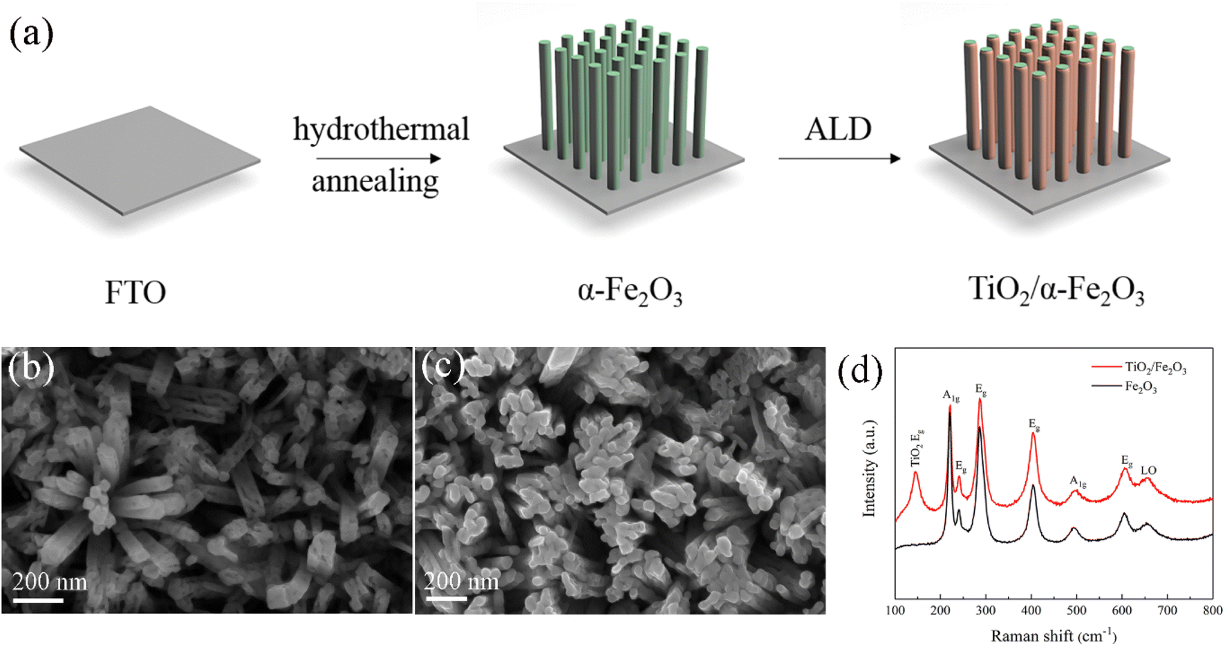 | ||
| Fig. 1 (a) Schematic view of the synthesis process for TiO2/α-Fe2O3 hierarchical nanostructure. (b) SEM images of pristine hematite nanorods, (c) SEM images of 40ALD cycles of TiO2 deposited on pristine hematite, (d) Raman-active modes of pristine hematite and TiO2 deposited on hematite. | ||
The phase composition and structure of β-FeOOH and α-Fe2O3 were characterized by XRD (Fig. S1, ESI†). The diffraction peak at 35.2° of 2θ can be assigned to the (211) reflection of tetragonal FeOOH (JCPDS 34-1266, red line). The diffraction peaks located at 35.9° and 64.5° can be ascribed to the (110) and (300) reflections of α-Fe2O3, respectively (COD 96-901-5504, black line). In addition, the reflections located at 26.6°, 33.9°, 38.0°, 51.8°, 61.9° and 66.0° and marked with asterisks correspond to the (110), (101), (200), (211), (130) and (301) reflections of the cassiterite phase of SnO2, respectively. Both samples show the characteristic signals of SnO2, which come from the FTO substrate.
The morphology and microstructure of β-FeOOH and hematite nanorods were thoroughly investigated by TEM (Fig. S2, ESI†). The typical solid β-FeOOH nanorods are uniform, with diameters ranging from 40 to 80 nm (Fig. S2a and b, ESI†). The main rings in the selected area electron diffraction (SAED) pattern correspond to the (200), (310) and (211) planes for tetragonal FeOOH (Fig. S2c, ESI†). Fig. S2d and e of the ESI† illustrate TEM images of pristine hematite nanorods. The concentric rings in the SAED corresponding to the (102), (104), (110) and (113) planes can be indexed to hematite, indicating the polycrystalline structure of Fe2O3 (Fig. S2f, ESI†).
The morphology and homogeneity of the pristine and TiO2-coated hematite samples were examined by FESEM. Fig. 1b displays that the pristine hematite nanorods are vertically aligned on the FTO. The diameter of the nanorods is around 60 to 80 nm. The SEM images of TiO2-40/Fe2O3 demonstrate a well-preserved hematite morphology (Fig. 1c). However, it is difficult to distinguish the TiO2 film because of its low thickness. The composition of the hematite before and after ALD-TiO2 coating was confirmed by Raman spectra (Fig. 1d). The Raman peaks at 220, 241, 286, 404, 494 and 606 cm−1 are assigned to the hematite structure. The LO peak center at 658 cm−1 is detected, which is attributed to the disorder-induced breaking of Raman symmetry properties.14,35 After TiO2 deposition, an intense Raman peak located at 144 cm−1 is observed, which can be indexed to the Eg mode of anatase TiO2.19 The Raman peaks of the Fe2O3 nanorods are not affected by ALD of TiO2.
The HRTEM images of TiO2-coated Fe2O3 nanorods with a different number of ALD cycles (from 10 to 150 cycles) is shown in Fig. S3, ESI.† At 10 ALD cycles, a continuous TiO2 film coverage cannot be clearly observed due to the small amount of TiO2 coating (Fig. S3a, ESI†). After 20 ALD cycles, Fe2O3 nanorods are homogeneously and uniformly coated with an ultrathin TiO2 film (Fig. S3b–e, ESI,† red dotted lines). The thicknesses of the TiO2 on Fe2O3 nanorods increase with the further increase of the number of ALD cycles. Fig. S3f of ESI† shows the lattice fringes of TiO2-150/Fe2O3 match well with the interplanar distance of the TiO2 anatase structure. The calculated lattice spacing of 0.35 nm can be assigned to the interplanar distance of the (011) plane of TiO2.
The HAADF-STEM images and the corresponding elemental mappings for all the TiO2-coated hematite samples are shown in Fig. 2. Fig. 2a shows small TiO2 nuclei randomly deposited on hematite nanorods after 10 ALD cycles. As the deposition proceeds, small nuclei grow up, and small nanocrystallites coalesce together to form a very thin, continuous TiO2 layer. The HAADF-STEM images of TiO2-20/Fe2O3, TiO2-40/Fe2O3, TiO2-80/Fe2O3 and TiO2-150/Fe2O3 show a conformal and homogeneous TiO2 deposition on the Fe2O3 nanorods, where the phases of TiO2 can be easily identified because of their different Z-contrast. The average thickness of the TiO2 film is calculated as 1.7, 3.5, 6.8, and 13.2 nm for 20, 40, 80 and 150 ALD cycles, respectively (Fig. 2b–e). This indicates that the shell thickness of the TiO2 coatings versus the number of ALD cycles shows good linearity with a slope corresponding to a growth per cycle (GPC) of 0.88 Å. The thickness of the TiO2 overlayer from TEM images is well-controlled and shows the same trend as the ellipsometry data on Si wafers (Table S1, ESI†). The corresponding elemental maps further elucidate a homogenous distribution of Ti and O elements on the Fe2O3 nanorods. The EDX spectra for the pristine Fe2O3 and TiO2-20/Fe2O3, further indicates the presence of both Fe and Ti elements (Fig. S4, ESI†). The atomic/weight percentage of all the samples with different ALD cycles are summarized in Table S2 of ESI.†
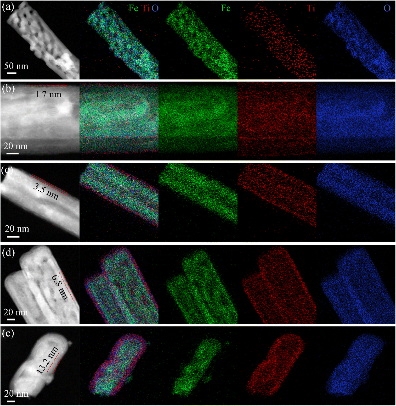 | ||
| Fig. 2 HAADF-STEM and corresponding EDX elemental maps for (a) TiO2-10/Fe2O3, (b) TiO2-20/Fe2O3, (c) TiO2-40/Fe2O3, (d) TiO2-80/Fe2O3 and (e) TiO2-150/Fe2O3. | ||
The optical properties of the pristine TiO2 on FTO substrate, pristine hematite and TiO2-coated hematite were measured by UV-vis-NIR diffuse reflectance spectroscopy (Fig. S5, ESI†). As expected, TiO2 shows a high absorbance in the UV region, while Fe2O3 and TiO2/Fe2O3 show a high absorbance in the visible region (Fig. S5a, ESI†). Fig. S5b–d in the ESI† shows the estimated optical band gap, which can be measured from the plot of (F(R)·hν)1/2versus hν.36 The band gaps obtained from Tauc-plots for pristine TiO2, pristine Fe2O3 and TiO2/Fe2O3 are around 3.25, 2.07 and 2.02 eV, respectively, that match well with the reported values.4,10 The slight change of band gap between Fe2O3 and TiO2/Fe2O3 indicates that the doping of Ti in hematite is negligible.
The surface composition and chemical states of the samples were investigated by high-resolution XPS (Fig. S6, ESI†). The survey spectra of pristine TiO2, pristine hematite and hematite coated with 20 TiO2 ALD cycles are shown in Fig. S6a, ESI,† confirming the presence of all expected elements. Fig. S6b of ESI† shows the Fe 2p peaks of the pristine Fe2O3 and TiO2-coated Fe2O3. The iron peaks are still well visible for the TiO2-20/Fe2O3 sample, indicating that the TiO2 layer is sufficiently thin, which is in good agreement with TEM measurements. The two peaks located at binding energies of 711.9 and 725.1 eV can be assigned to Fe 2p3/2 and Fe 2p1/2 of hematite, respectively, indicating the oxidation state III of iron.37,38 XPS spectrum of O 1s peak for hematite samples is centered at 530.2 eV, which is consistent with literature values (Fig. S6c, ESI†).21,39
To determine the energy level offset at the α-Fe2O3/TiO2 heterostructures, the Kraut's method was used, as a direct measurement of the valence band offsets is typically difficult due to overlapping valence band signals.40,41 Assuming the energy difference between the valence band and the core levels is the same for the pristine materials and the heterostructure, the valence band offset in the heterostructure  can be calculated with the following equation:
 | (1) |
The corresponding core level and valence spectra are shown in Fig. 3a–d.
While the binding energy of the core levels was determined from the peak position after fitting, the valence band onsets were determined from a linear extrapolation of the leading edges. This results in a valence band offset of 0.83 eV, with the valence band of α-Fe2O3 being closer to the Fermi-level. Considering the band gaps determined by absorption spectroscopy (Fig. S5, ESI†), we find that the α-Fe2O3/TiO2 interface forms a straddling gap (type I heterostructure) with a conduction band offset of 0.35 eV (Fig. 3e).
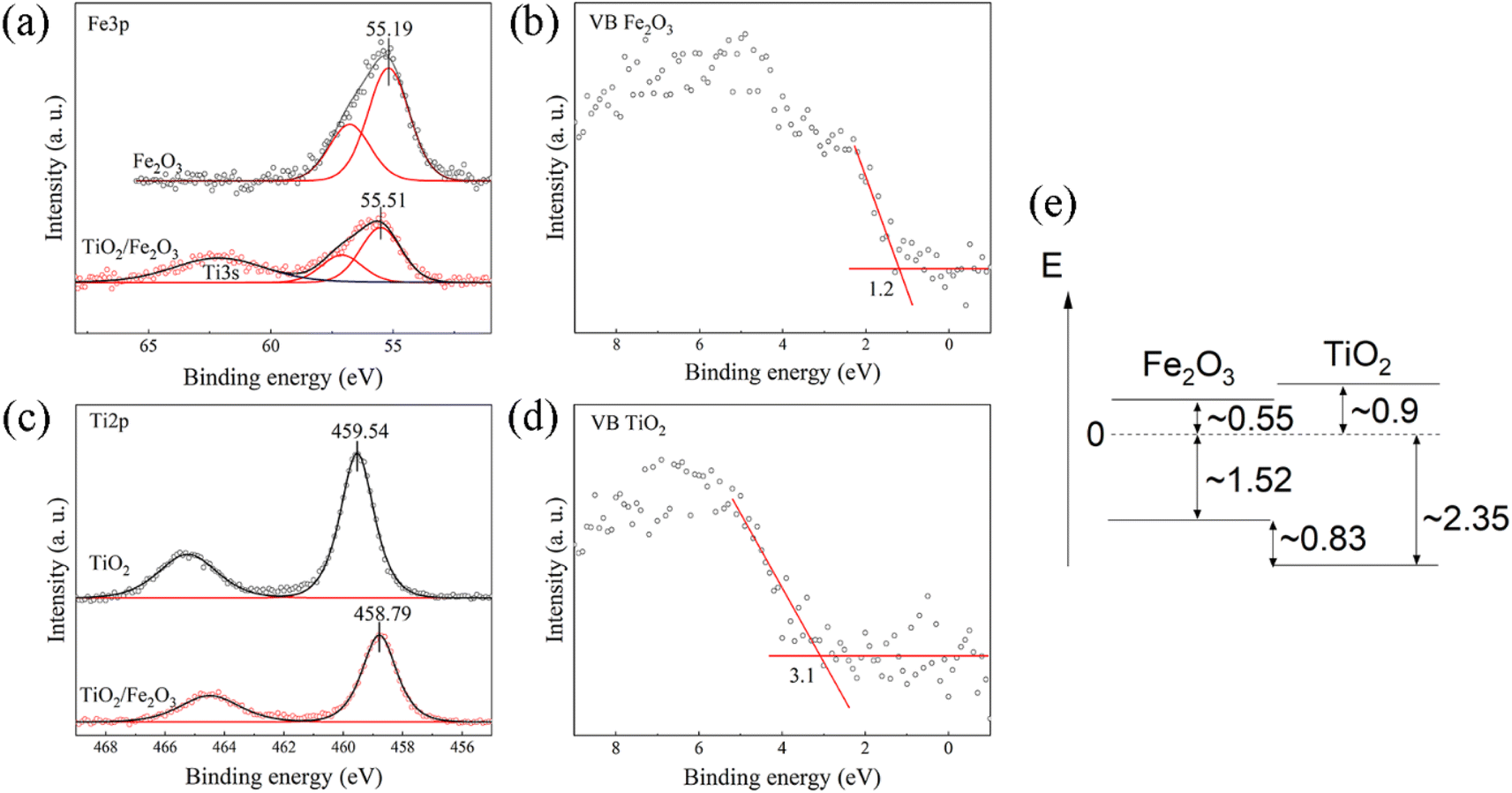 | ||
| Fig. 3 (a) Fe 3p core level spectra of Fe2O3 (black) and TiO2-20/Fe2O3 (red). Shirley backgrounds have been removed. (b) Valence band spectrum of Fe2O3 with a linear extrapolation of the valence band onset. (c) Ti 2p core level spectra of TiO2 (black) and TiO2-20/Fe2O3 (red). Shirley backgrounds have been removed. (d) Valence band spectrum of TiO2 with a linear extrapolation of the valence band onset. (e) Schematic energy level diagram of TiO2/Fe2O3. | ||
3.2 Photoelectrochemical activities
The PEC performance was measured on pristine hematite and hematite modified with various thicknesses of the TiO2 overlayer (Fig. 4). Fig. 4a shows the photocurrent–potential (J–V) curves of hematite photoanodes under visible light. Compared to pristine hematite, the photoanodes of TiO2-coated hematite show an obvious lower overpotential for water oxidation reaction and a cathodic shift of the onset potential. Furthermore, the photocurrent density shows a significant enhancement by deposition of the TiO2 overlayer.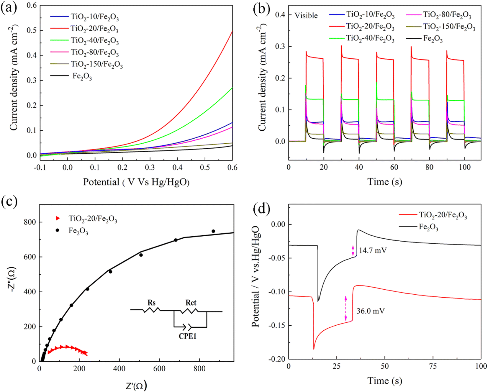 | ||
| Fig. 4 (a) Photocurrent versus potential plots of a different number of ALD cycles for TiO2 coated hematite photoanodes under visible light irradiation. (b) Time-based photocurrent density at 0.5 V bias vs. Hg/HgO with the light off and on for 10 s. (c) Nyquist plots of pristine Fe2O3 and TiO2-20/Fe2O3 photoanodes measured under light illumination. (d) OCV curves of pristine Fe2O3 and TiO2-20/Fe2O3 photoanodes with the light on for 20 s. | ||
To further study the impact of the TiO2 overlayer on hematite photoanodes on the PEC performance, the measurement of the photocurrent response under visible light at 0.5 V bias vs. Hg/HgO (1.4 V vs. RHE) was carried out on all the samples (Fig. 4b). As mentioned above, Fe2O3 can be excited to produce photogenerated electron–hole pairs under visible light due to the low band gap, while TiO2 shows almost no photocurrent response because of its large band gap. Therefore, the photocurrent response is attributed only to Fe2O3 under visible light. The photocurrent density of pristine hematite is 0.01 mA cm−2. The low photocurrent response is due to the high recombination rate of photogenerated charge carriers. By the deposition of the TiO2 overlayer, all the composite samples display improved photocurrent densities, which can be attributed to the passivation effect of TiO2.18,42 It is well known that the passivation layer is normally very thin (<100 nm), which can prevent parasitic light absorption and charge-transfer inhibition.43 TiO2 passivates the surface states, reduces the recombination rate of the photogenerated electron–hole pairs, facilitates photogenerated hole transfer and improves the photocurrent response.22 The photocurrent densities of TiO2 coated hematite with 10, 20, 40, 80 and 150 ALD cycles are 0.06, 0.27, 0.13, 0.06 and 0.02 mA cm−2, respectively. The highest photocurrent response is recorded for TiO2-20/Fe2O3 (∼1.7 nm), showing a photocurrent density ca. 27 times higher than that obtained for the pristine hematite. At this optimized thickness, the TiO2 overlayer passivates surface recombination states of hematite and the photogenerated holes can be transferred from hematite to electrolyte. With a further increase of the TiO2 thickness, the TiO2 overlayer can hinder the hole transfer efficiency and block light from entering the inner hematite layer, leading to a dramatic decrease in photocurrent response.
During visible light illumination, photogenerated holes in pristine hematite travel to the semiconductor/liquid junction (SCLJ) and accumulate there, owing to the existence of surface trap states. This leads to the appearance of large anodic transient peaks, which decay until they finally reach an equilibrium between charge carrier transfer and recombination at the interface.44 On the other hand, cathodic transient peaks overshoot and decay back to zero under dark conditions, which are attributed to the electrons diffusing from the external circuit and recombining with holes accumulated at the SCLJ.12,22 However, the transient photocurrent spike decreases obviously after the deposition of TiO2. Moreover, the feature was highly repeatable for numerous ALD cycles. This result further demonstrates the passivation effect of the TiO2 overlayer. Therefore, Fe2O3 essentially acts as a light absorption layer, absorbing the visible light and producing photogenerated electron–hole pairs.
EIS was measured under light illumination to study the interfacial kinetics of the charge transfer process. Fig. 4c displays the Nyquist plots of pristine Fe2O3 and TiO2-20/Fe2O3 that are simulated using the equivalent circuit (EC) shown in Fig. 4c inset. The equivalent circuit elements include the series resistance in the PEC cell (Rs), the charge transfer resistance (Rct) at the Fe2O3/electrolyte interface and a constant phase element (CPE1).39,45 The fitting parameters for the equivalent circuit elements are shown in Table 1. Compared to pristine hematite, TiO2-20/Fe2O3 has a lower charge transfer resistance than pristine hematite, which indicates that the charge transfer across hematite/electrolyte interface is significantly facilitated due to the passivation effect of TiO2. The EIS result confirms that TiO2/Fe2O3 heterostructure can significantly enhance the charge transfer and separation and improve the PEC water splitting performance.
| R s (Ω cm2) | R ct (Ω cm2) | |
|---|---|---|
| Pristine-Fe2O3 | 7.5 | 247.3 |
| TiO2-20/Fe2O3 | 13.9 | 1807.0 |
The open circuit voltage (OCV) of pristine hematite and hematite coated with 20 TiO2 ALD cycles were measured in the dark and illumination conditions to study the behavior of the photogenerated carriers (Fig. 4d). Under illumination, the value of pristine Fe2O3 moves to a negative potential, while the potential of TiO2-20/Fe2O3 shifts more negative than pristine Fe2O3. This suggests that both samples are n-type semiconductors, in line with the XPS results.46–48 Under illumination, both samples exhibit a similar trend and create a similar number of photogenerated electrons, which can accumulate on the surface of photoanodes, leading to a potential negative shift and a sudden increase in the OCV. Meanwhile, the recombination of photogenerated electrons and holes occurs, which leads to a decrease of the OCV until a relatively steady state is reached. It can be seen that the potential change for Fe2O3 and TiO2-20/Fe2O3 is comparable. However, compared to pristine Fe2O3, the photoanode of TiO2-20/Fe2O3 is more stable due to the passivation effect of TiO2 and the low photogenerated carrier recombination dynamics. After irradiation for 20 seconds, the light is turned off, and the OCV continues to decline due to the high recombination of photoelectron–hole pairs. The photovoltages of the pristine Fe2O3 and TiO2-20/Fe2O3 photoanodes are 14.7 mV and 36.0 mV, respectively, as obtained from the difference between the OCV under dark and light conditions. Compared to pristine Fe2O3, the photovoltage obtained with TiO2-20/Fe2O3 is much higher due to the fact that more photogenerated electrons are collected and a more efficient separation of the photogenerated electron–hole pairs.
To study the photo-response properties further, the incident photon to converted electron (IPCE) and stability test of pristine and TiO2-coated hematite photoanodes were measured under visible light. The IPCE values have been calculated according to the equation:
 | (2) |
A maximum IPCE of 1.35% at 430 nm is achieved by TiO2-20/Fe2O3, which is much higher than the corresponding value of 0.05% for pristine Fe2O3 photoanodes (Fig. S7a, ESI†). The significant improvement of photoconversion efficiency indicates higher utilization efficiency of photoinduced carriers for the TiO2-coated hematite photoanodes, which is consistent with the J–V measurements (Fig. 4a).
Applied bias photon-to-current efficiency (ABPE) was calculated from the photocurrent–potential plots according to the following equation:
 | (3) |
The ABPE was plotted as a function of the applied potential. The TiO2-20/Fe2O3 photoanode achieves the maximum ABPE value of 0.01% at 1.02 V, which is significantly higher than that of 0.004% at 0.98 V for pristine hematite electrode (Fig. S7b, ESI†). Clearly, the improvement of PEC water splitting performance can be attributed to the enhanced charge separation caused by the passivation effect of TiO2.
Fig. S8 in ESI† shows the current retention as a function of the time of pristine hematite and hematite coated with 20 TiO2 ALD cycles under continuously visible light irradiation for 60 min. A significant improvement of the photocurrents of pristine hematite electrode upon TiO2 deposition as well as a good stability can be obtained. The morphology and the composition of the synthesized photocatalyst after stability test are well maintained, which are shown in Fig. S9 and S10 in ESI.†
Fig. S11 in ESI† shows the Mott–Schottky plots of the pristine Fe2O3 and TiO2-20/Fe2O3. The slopes determined from the Mott–Schottky plots are used to estimate the carrier densities. The positive slopes display the n-type semiconductor nature of the pristine Fe2O3 and TiO2-20/Fe2O3. Moreover, the plot of TiO2-20/Fe2O3 depicts a suppressed slope compared to pristine Fe2O3, suggesting a higher carrier concentration in the heterostructure than in the pristine Fe2O3. The as-calculated carrier densities for pristine Fe2O3 and TiO2-20/Fe2O3 are 1.6 × 1019 cm−3 and 4.4 × 1019 cm−3, respectively.
Contrary to the visible light system, both Fe2O3 and TiO2 participate in the photocurrent response under UV light irradiation due to the suitable band gap of Fe2O3 and TiO2. As a result, the photocurrent response is not only attributed to Fe2O3 but is also related to the TiO2 overlayer. To verify the role of TiO2 overlayer in the PEC performance of hematite, the photocurrent response for hematite and TiO2-coated hematite samples were evaluated under UV light (Fig. S12, ESI†).
The experimental results show that the photocurrent response varies significantly with the thickness of the TiO2 overlayer. Compared to pristine hematite, the TiO2 overlayer results in a remarkable enhancement of photocurrent response. Before 80 ALD cycles, the variation trend of the photocurrent response of hematite samples with TiO2 thickness under UV irradiation was similar to that under visible light irradiation. The photocurrent densities of pristine hematite and TiO2 coated hematite with 10, 20, 40 and 80 ALD cycles are 0.03, 0.07, 0.41, 0.22 and 0.09 mA cm−2, respectively. The optimized TiO2-20/Fe2O3 (ca. 1.7 nm) shows a photocurrent response of 0.41 mA cm−2, which is 14 times higher than the photocurrent response of the pristine hematite. TiO2 thicknesses up to 1.7–6.8 nm (20 ALD cycles to 80 ALD cycles) lead to a decrease in photocurrent response. At this stage, the TiO2 overlayer mainly acts as a passivation layer and Fe2O3 acts as a light absorption layer. However, the photocurrent response increases with a further increase of the thickness of the TiO2 overlayer (i.e., from 6.8 to 13.2 nm, 80 ALD to 150 ALD), in contrast to what was observed under visible light. The photocurrent density of TiO2-150/Fe2O3 is 0.14 mA cm−2. This change of photocurrent response at a higher thickness suggests that the photocurrent response is not dominated by Fe2O3 anymore, but is restricted to the TiO2 overlayer.
Fig. 5 compares the photocurrent response of hematite samples coated with different thicknesses of the TiO2 overlayer under different illumination. The experimental results reveal a substantial variation of the photocurrent response as a function of the thickness of the TiO2 overlayer. The highest photocurrent response exhibited by the TiO2-20/Fe2O3 photoanodes is recorded under both visible and UV light. After 20ALD cycles, the photocurrent response decreases with a further increase of the TiO2 thickness under visible light, while it first decreases and then increases under UV light.
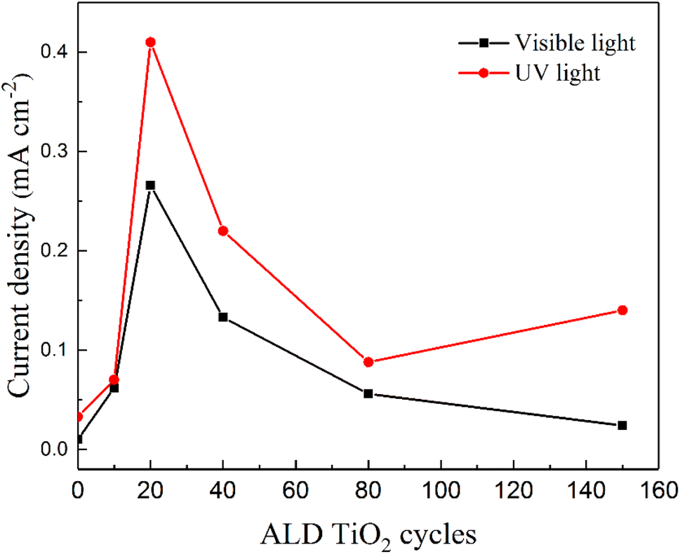 | ||
| Fig. 5 Current densities of hematite photoanodes with different ALD TiO2 cycles at 0.5 V bias vs. Hg/HgO, 1 M KOH, under visible light and UV light irradiation, respectively. | ||
Under visible light, the TiO2 overlayer acts as a passivation layer. The photogenerated holes from Fe2O3 can cross the passivation layer primarily by tunneling, which gradually vanishes within a few nanometers.43,50,51 Because of this mechanism, the TiO2 overlayer must be of the optimal thickness. It should not be too thin to passivate the surface recombination states enough, and not too thick to allow the photogenerated holes transfer between Fe2O3 and electrolyte to participate in the water oxidation. Under UV light, when the TiO2 thickness is ≤6.8 nm, it does not absorb enough UV light, and therefore only few photogenerated charge pairs are produced in the TiO2. In this case, TiO2 mainly acts as a passivation layer, and the photocurrent response is dominated by Fe2O3. Therefore, the photocurrent response under UV light follows the same trend as under visible light. However, when the thickness of TiO2 is larger than the optimal 1.7 nm (20 ALD cycles), it hinders the transfer of the photogenerated holes. Therefore, the photogenerated holes in Fe2O3 cannot efficiently cross the TiO2 overlayer. Conversely, when the TiO2 overlayer is thick enough, it absorbs more UV light and produces more photogenerated charge pairs that participate in water oxidation. The contribution of the TiO2 overlayer for photocurrent response becomes dominant at 150 ALD cycles (13.2 nm). At this stage, TiO2 mainly behaves as the active layer, and the contribution of Fe2O3 becomes negligeable. This demonstrates that the photoresponse under UV illumination is largely related to the thickness of the TiO2 overlayer.
3.3 Charge transfer mechanism
Fig. 6 displays the schematic diagram of the charge separation and transport mechanism under visible and UV light illumination. Under visible light, Fe2O3 with a suitable band gap can produce photogenerated electrons in the conduction band and photogenerated holes in the valence band. The photogenerated electrons driven by the bias voltage will transfer through the external circuit (Fig. 6a). The photogenerated holes from Fe2O3 cannot be transferred to the valence band of TiO2 owing to an unfavorable valence band edge alignment of Fe2O3 and TiO2. Therefore, TiO2 behaves as a passivation layer and Fe2O3 acts as a light absorption layer. In the case of UV light illumination, both Fe2O3 and TiO2 have suitable band gaps that can be excited to produce electron–hole pairs. The photogenerated electrons of TiO2 migrate to the conduction band of Fe2O3, which lies at a more positive potential than that of TiO2. Subsequently, the electrons in Fe2O3 flow into the external circuit. The photoinduced holes in Fe2O3 can pass through the TiO2 thin layer by tunneling effect for the oxidation reaction. The photogenerated holes from TiO2 can react directly with the electrolyte. It can also transfer to the valence band of Fe2O3 and then cross the TiO2 thin layer to participate in the water oxidation reaction (Fig. 6b). This indicates that the photocurrent response is not always governed by the Fe2O3. The TiO2 overlayer also plays an essential role in producing photocurrent response under UV light. As we have discussed above, the impact of the TiO2 overlayer is largely dependent on the film thickness.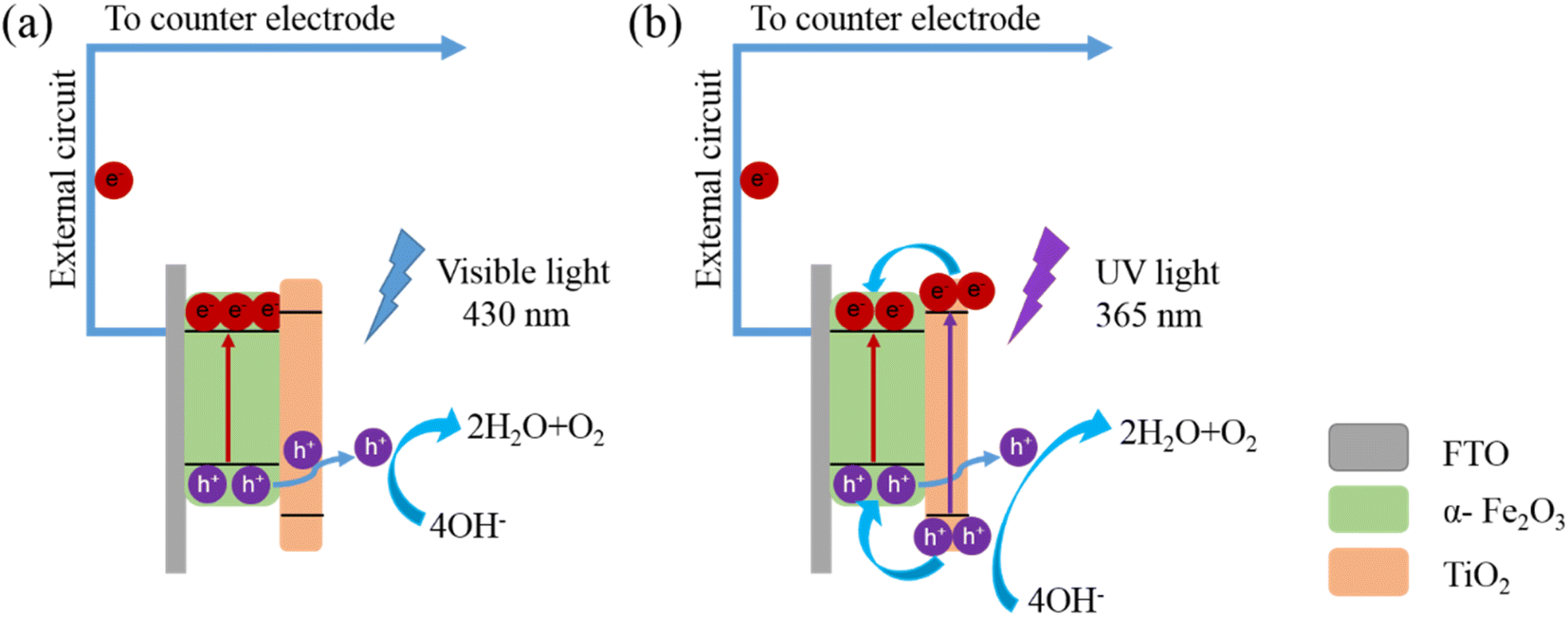 | ||
| Fig. 6 Schematic illustration of the charge-transfer pathways in the TiO2/Fe2O3 system under visible light and UV light. | ||
4. Conclusion
TiO2/Fe2O3 heterostructures have been synthesized by a hydrothermal method and atomic layer deposition. The as-synthesized samples show a homogeneous and conformal coating of TiO2 onto the hematite nanorods. The morphology and thickness of a TiO2 overlayer can be precisely controlled. The pristine hematite and hematite coated with various thicknesses of TiO2 are studied for their photocurrent response under visible and UV light. Compared to pristine hematite, the TiO2 coating leads to a significant improvement in photocurrent response. The photocurrent response of the TiO2/Fe2O3 heterostructures is strictly related to the thickness of the TiO2 overlayer. The best photoanode response is observed with a coating of 1.7 nm (TiO2-20/Fe2O3) under both visible and UV light. Our results show that the photocurrent density of TiO2-20/Fe2O3 reaches 0.27 mA cm−2 at 0.5 V vs. Hg/HgO under visible light, which is 27 times higher than that of pristine α-Fe2O3. Under visible light, the TiO2 overlayer acts as a passivation layer facilitating the photogenerated holes transfer and reducing the surface recombination rate of electron–hole pairs. Fe2O3 is the major contributor to the photogeneration of electron–hole pairs. Under UV light, the TiO2 overlayer behaves mainly as a passivation layer at lower thicknesses (≤6.8 nm). At higher thickness, TiO2 acts as a light absorption layer, while the contribution of Fe2O3 is reduced. This work not only provides deep insights into the impact of a TiO2 overlayer on the PEC water splitting performance of hematite, but can be also valuable and promising for the design and development of high-performance photoanodes.Data availability
The data supporting this article have been included as part of the ESI.†Conflicts of interest
There are no conflicts to declare.Acknowledgements
J. Wang and L. Liccardo contributed equally to this work. J. Wang acknowledges the fellowship from the China Scholarship Council (CSC). C. Erdmann is acknowledged for the TEM measurement. C. X. Shen is acknowledged for Raman measurement. E. Wierzbicka would like to acknowledge the Polish National Agency For Academic Exchange, Polish Returns Programme (project no. BPN/PPO/2021/1/00002) for the financial support of the project.References
- K. B. Ibrahim, T. A. Shifa, M. Bordin, E. Moretti, H. L. Wu and A. Vomiero, Confinement Accelerates Water Oxidation Catalysis: Evidence from In Situ Studies, Small Methods, 2023, 7(10), 2300348 CrossRef CAS PubMed.
- K. B. Ibrahim, T. A. Shifa, P. Moras, E. Moretti and A. Vomiero, Facile Electron Transfer in Atomically Coupled Heterointerface for Accelerated Oxygen Evolution, Small, 2022, 19(1), 2204765 CrossRef PubMed.
- Y. W. Phuan, W. J. Ong, M. N. Chong and J. D. Ocon, Prospects of electrochemically synthesized hematite photoanodes for photoelectrochemical water splitting: A review, J. Photochem. Photobiol., C, 2017, 33, 54–82 CrossRef CAS.
- Y. Yang, S. Niu, D. Han, T. Liu, G. Wang and Y. Li, Progress in Developing Metal Oxide Nanomaterials for Photoelectrochemical Water Splitting, Adv. Energy Mater., 2017, 7(19), 1700555 CrossRef.
- J. Joy, J. Mathew and S. C. George, Nanomaterials for photoelectrochemical water splitting – review, Int. J. Hydrogen Energy, 2018, 43(10), 4804–4817 CrossRef CAS.
- S. Kment, F. Riboni, S. Pausova, L. Wang, L. Wang, H. Han, Z. Hubicka, J. Krysa, P. Schmuki and R. Zboril, Photoanodes based on TiO2 and alpha-Fe2O3 for solar water splitting - superior role of 1D nanoarchitectures and of combined heterostructures, Chem. Soc. Rev., 2017, 46(12), 3716–3769 RSC.
- M. Mishra and D. M. Chun, α-Fe2O3 as a photocatalytic material: A review, Appl. Catal., A, 2015, 498, 126–141 CrossRef CAS.
- L. Li, Y. Yu, F. Meng, Y. Tan, R. J. Hamers and S. Jin, Facile solution synthesis of alpha-FeF3.3H2O nanowires and their conversion to alpha-Fe2O3 nanowires for photoelectrochemical application, Nano Lett., 2012, 12(2), 724–731 CrossRef CAS.
- C. Li, A. Li, Z. Luo, J. Zhang, X. Chang, Z. Huang, T. Wang and J. Gong, Surviving High-Temperature Calcination: ZrO2 -Induced Hematite Nanotubes for Photoelectrochemical Water Oxidation, Angew. Chem., 2017, 56(15), 4150–4155 CrossRef CAS.
- M. Ji, J. Cai, Y. Ma and L. Qi, Controlled Growth of Ferrihydrite Branched Nanosheet Arrays and Their Transformation to Hematite Nanosheet Arrays for Photoelectrochemical Water Splitting, ACS Appl. Mater. Interfaces, 2016, 8(6), 3651–3660 CrossRef CAS PubMed.
- Y. Li, X. Wei, B. Zhu, H. Wang, Y. Tang, T. Sum and X. Chen, Hierarchically branched Fe2O3@TiO2 nanorod arrays for photoelectrochemical water splitting: facile synthesis and enhanced photoelectrochemical performance, Nanoscale, 2016, 8(21), 11284–11290 RSC.
- X. Yang, R. Liu, C. Du, P. Dai, Z. Zheng and D. Wang, Improving hematite-based photoelectrochemical water splitting with ultrathin TiO2 by atomic layer deposition, ACS Appl. Mater. Interfaces, 2014, 6(15), 12005–12011 CrossRef CAS PubMed.
- K. Y. Yoon, J. S. Lee, K. Kim, C. H. Bak, S. I. Kim, J. B. Kim and J. H. Jang, Hematite-based photoelectrochemical water splitting supported by inverse opal structures of graphene, ACS Appl. Mater. Interfaces, 2014, 6(24), 22634–22639 CrossRef CAS PubMed.
- L. Palmolahti, H. Ali-Löytty, R. Khan, J. Saari, N. V. Tkachenko and M. Valden, Modification of Surface States of Hematite-Based Photoanodes by Submonolayer of TiO2 for Enhanced Solar Water Splitting, J. Phys. Chem. C, 2020, 124(24), 13094–13101 CrossRef CAS.
- R. Franking, L. Li, M. A. Lukowski, F. Meng, Y. Tan, R. J. Hamers and S. Jin, Facile post-growth doping of nanostructured hematite photoanodes for enhanced photoelectrochemical water oxidation, Energy Environ. Sci., 2013, 6(2), 500–512 RSC.
- L. Liccardo, E. Lushaj, L. D. Compare, E. Moretti and A. Vomiero, Nanoscale ZnO/α-Fe2O3 Heterostructures: Toward Efficient and Low-Cost Photoanodes for Water Splitting, Small Sci., 2021, 2100104 Search PubMed.
- D. Barreca, G. Carraro, A. Gasparotto, C. Maccato, M. E. A. Warwick, K. Kaunisto, C. Sada, S. Turner, Y. Gönüllü, T. P. Ruoko, L. Borgese, E. Bontempi, G. Van Tendeloo, H. Lemmetyinen and S. Mathur, Fe2O3–TiO2 Nano-heterostructure Photoanodes for Highly Efficient Solar Water Oxidation, Adv. Mater. Interfaces, 2015, 2, 1500313 CrossRef.
- S. S. Mali, C. S. Shim, H. K. Park, J. Heo, P. S. Patil and C. K. Hong, Ultrathin Atomic Layer Deposited TiO2 for Surface Passivation of Hydrothermally Grown 1D TiO2 Nanorod Arrays for Efficient Solid-State Perovskite Solar Cells, Chem. Mater., 2015, 27(5), 1541–1551 CrossRef.
- X. Li, P. S. Bassi, P. P. Boix, Y. Fang and L. H. Wong, Revealing the Role of TiO2 Surface Treatment of Hematite Nanorods Photoanodes for Solar Water Splitting, ACS Appl. Mater. Interfaces, 2015, 7(31), 16960–16966 CrossRef.
- D. Wang, Y. Chen, Y. Zhang, X. Zhang, N. Suzuki and C. Terashima, Boosting photoelectrochemical performance of hematite photoanode with TiO2 underlayer by extremely rapid high temperature annealing, Appl. Surf. Sci., 2017, 422, 913–920 CrossRef.
- F. Feng, C. Li, J. Jian, X. Qiao, H. Wang and L. Jia, Boosting hematite photoelectrochemical water splitting by decoration of TiO2 at the grain boundaries, Chem. Eng. J., 2019, 368, 959–967 CrossRef.
- M. G. Ahmed, I. E. Kretschmer, T. A. Kandiel, A. Y. Ahmed, F. A. Rashwan and D. W. Bahnemann, A Facile Surface Passivation of Hematite Photoanodes with TiO2 Overlayers for Efficient Solar Water Splitting, ACS Appl. Mater. Interfaces, 2015, 7(43), 24053–24062 CrossRef PubMed.
- T. Imrich, R. Zazpe, H. Krýsová, Š. Paušová, F. Dvorak, J. Rodriguez-Pereira, J. Michalicka, O. Man, J. M. Macak, M. Neumann-Spallart and J. Krýsa, Protection of hematite photoelectrodes by ALD-TiO2 capping, J. Photochem. Photobiol., A, 2021, 409, 113126 CrossRef.
- R. Mechiakh, N. B. Sedrine, R. Chtourou and R. Bensaha, Correlation between microstructure and optical properties of nano-crystalline TiO2 thin films prepared by sol–gel dip coating, Appl. Surf. Sci., 2010, 257(3), 670–676 CrossRef.
- V. Bukauskas, S. Kaciulis, A. Mezzi, A. Mironas, G. Niaura, M. Rudzikas, I. Šimkienė and A. Šetkus, Effect of substrate temperature on the arrangement of ultra-thin TiO2 films grown by a dc-magnetron sputtering deposition, Thin Solid Films, 2015, 585, 5–12 CrossRef.
- J. Wang, Z. Yin, F. Hermerschmidt, E. J. W. List-Kratochvil and N. Pinna, Impact of Different Intermediate Layers on the Morphology and Crystallinity of TiO2 Grown on Carbon Nanotubes by Atomic Layer Deposition, Adv. Mater. Interfaces, 2021, 8(15), 2100759 CrossRef CAS.
- C. Marichy and N. Pinna, Carbon-nanostructures coated/decorated by atomic layer deposition: Growth and applications, Coord. Chem. Rev., 2013, 257(23–24), 3232–3253 CrossRef CAS.
- N. Pinna and M. Knez, Atomic Layer Deposition of Nanostructured Materials, Wiley-VCH, 2011, pp. 1–435 Search PubMed.
- M. Leskelä and M. Ritala, Atomic layer deposition (ALD) from precursors to thin film structures, Thin Solid Films, 2002, 409, 138–146 CrossRef.
- C. Marichy and N. Pinna, Atomic Layer Deposition to Materials for Gas Sensing Applications, Adv. Mater. Interfaces, 2016, 3(21), 1600335 CrossRef.
- C. Marichy, M. Bechelany and N. Pinna, Atomic layer deposition of nanostructured materials for energy and environmental applications, Adv. Mater., 2012, 24(8), 1017–1032 CrossRef CAS PubMed.
- Y. Xia and L. Yin, Core-shell structured alpha-Fe2O3@TiO2 nanocomposites with improved photocatalytic activity in the visible light region, Phys. Chem. Chem. Phys., 2013, 15(42), 18627–18634 RSC.
- K. Yao, P. Basnet, H. Sessions, G. K. Larsen, S. E. H. Murph and Y. Zhao, Fe2O3–TiO2 core–shell nanorod arrays for visible light photocatalytic applications, Catal. Today, 2016, 270, 51–58 CrossRef CAS.
- N. Fairley, V. Fernandez, M. Richard-Plouet, C. Guillot-Deudon, J. Walton, E. Smith, D. Flahaut, M. Greiner, M. Biesinger, S. Tougaard, D. Morgan and J. Baltrusaitis, Systematic and collaborative approach to problem solving using X-ray photoelectron spectroscopy, Appl. Surf. Sci. Adv., 2021, 5, 100112 CrossRef.
- Y. Liu and R. D. L. Smith, Differentiating Defects and Their Influence on Hematite Photoanodes Using X-ray Absorption Spectroscopy and Raman Microscopy, ACS Appl. Mater. Interfaces, 2022, 14(5), 6615–6624 CrossRef CAS.
- P. Makula, M. Pacia and W. Macyk, How To Correctly Determine the Band Gap Energy of Modified Semiconductor Photocatalysts Based on UV-Vis Spectra, J. Phys. Chem. Lett., 2018, 9(23), 6814–6817 CrossRef CAS PubMed.
- S. Liu, K. Yao, L. H. Fu and M. G. Ma, Selective synthesis of Fe3O4, γ-Fe2O3, and α-Fe2O3 using cellulose-based composites as precursors, RSC Adv., 2016, 6(3), 2135–2140 RSC.
- P. S. Bagus, C. J. Nelin, C. R. Brundle, N. Lahiri, E. S. Ilton and K. M. Rosso, Analysis of the Fe 2p XPS for hematite alpha Fe2O3: Consequences of covalent bonding and orbital splittings on multiplet splittings, J. Chem. Phys., 2020, 152(1), 014704 CrossRef CAS PubMed.
- X. Lv, S. Shao, Y. Xiao and J. Deng, One-step in-situ formation of TiO2 nanosheets interconnected hematite photoanode for enhanced water oxidation, Appl. Surf. Sci., 2021, 560, 150036 CrossRef CAS.
- E. A. Kraut, R. W. Grant, J. R. Waldrop and S. P. Kowalczyk, Precise Determination of the Valence-Band Edge in X-Ray Photoemission Spectra: Application to Measurement of Semiconductor Interface Potentials, Phys. Rev. Lett., 1980, 44(24), 1620–1623 CrossRef.
- T. Schultz, M. Kneiß, P. Storm, D. Splith, H. von Wenckstern, M. Grundmann and N. Koch, Band Offsets at κ-([Al,In]xGa1–x)2O3/MgO Interfaces, ACS Appl. Mater. Interfaces, 2020, 12(7), 8879–8885 CrossRef PubMed.
- Z. Xing, F. Ren, H. Wu, L. Wu, X. Wang, J. Wang, D. Wan, G. Zhang and C. Jiang, Enhanced PEC performance of nanoporous Si photoelectrodes by covering HfO2 and TiO2 passivation layers, Sci. Rep., 2017, 7, 43901 CrossRef PubMed.
- R. Liu, Z. Zheng, J. Spurgeon and X. Yang, Enhanced photoelectrochemical water-splitting performance of semiconductors by surface passivation layers, Energy Environ. Sci., 2014, 7(8), 2504–2517 RSC.
- F. Le Formal, N. Tétreault, M. Cornuz, T. Moehl, M. Grätzel and K. Sivula, Passivating surface states on water splitting hematite photoanodes with alumina overlayers, Chem. Sci., 2011, 2(4), 737–743 RSC.
- X. Chai, H. Zhang and C. Cheng, 3D FTO Inverse Opals@Hematite@TiO2 hierarchically structured Photoanode for Photoelectrochemical Water Splitting, Semicond. Sci. Technol., 2017, 32(11), 114003 CrossRef.
- Y. Ma, Y. Liu, Y. Bian, A. Zhu, Y. Yang and J. Pan, Controlling shape anisotropy of hexagonal CdS for highly stable and efficient photocatalytic H2 evolution and photoelectrochemical water splitting, J. Colloid Interface Sci., 2018, 518, 140–148 CrossRef PubMed.
- Z. Hao, M. Ruan, Z. Guo, W. Yan, X. Wu and Z. Liu, The synergistic role of the photosensitivity effect and extended space charge region in an inorganic–organic WO3/PANI photoanode for efficient PEC water splitting, Sustainable Energy Fuels, 2021, 5(11), 2893–2906 RSC.
- J. Kamimura, P. Bogdanoff, M. Ramsteiner, P. Corfdir, F. Feix, L. Geelhaar and H. Riechert, p-Type Doping of GaN Nanowires Characterized by Photoelectrochemical Measurements, Nano Lett., 2017, 17(3), 1529–1537 CrossRef CAS PubMed.
- C. Shen, E. Wierzbicka, T. Schultz, R. Wang, N. Koch and N. Pinna, Atomic Layer Deposition of MoS2 Decorated TiO2 Nanotubes for Photoelectrochemical Water Splitting, Adv. Mater. Interfaces, 2022, 2200643 CrossRef CAS.
- Z. Luo, T. Wang, J. Zhang, C. Li, H. Li and J. Gong, Dendritic Hematite Nanoarray Photoanode Modified with a Conformal Titanium Dioxide Interlayer for Effective Charge Collection, Angew. Chem., Int. Ed., 2017, 56(42), 12878–12882 CrossRef CAS PubMed.
- C. Marichy, N. Donato, M. Latino, M. G. Willinger, J. P. Tessonnier, G. Neri and N. Pinna, Gas sensing properties and p-type response of ALD TiO2 coated carbon nanotubes, Nanotechnology, 2015, 26(2), 024004 CrossRef CAS PubMed.
Footnote |
| † Electronic supplementary information (ESI) available. See DOI: https://doi.org/10.1039/d3se01633a |
| This journal is © The Royal Society of Chemistry 2024 |