AgInS2/CdSe type-II core/shell quantum dot-sensitized solar cells with an efficiency of 11.75% under 0.1 sun†
Received
25th September 2023
, Accepted 27th November 2023
First published on 27th November 2023
Abstract
We report the fabrication and photovoltaic performance of new type-II AgInS2/CdSe core/shell quantum dot-sensitized solar cells (QDSSCs). AgInS2 core and CdSe shell QDs are grown using the successive ionic layer adsorption and reaction (SILAR) method. X-ray diffraction reveals the orthorhombic and cubic structures for AgInS2 and CdSe, respectively. Optical spectra reveal the bandgaps of 1.91, 1.78, and 1.57 eV for AgInS2, CdSe, and AgInS2/CdSe, respectively. Cyclic voltammetry measurements show a type-II band alignment for the AgInS2/CdSe QDs. Liquid-junction AgInS2/CdSe QDSSCs are fabricated using a polysulfide electrolyte. Single-layered AgInS2 and CdSe QDSSCs are prepared simultaneously for comparison. The AgInS2/CdSe cell yields a PCE of 8.39% (Voc = 0.64 V, FF = 56.0%) under 1 sun, significantly higher than the single-layered AgInS2 (3.04%) and CdSe (3.67%) QDSSCs. Moreover, the Jsc increases from 7.72 in single-layered AgInS2 to 23.28 mA cm−2 in core/shell AgInS2/CdSe. The PCE of AgInS2/CdSe further increases to 11.75% under 0.1 sun. The PCE of 8.39% is comparable to the best PCE (8.26%) of Dy-doped CdTe/CdS for all type-II core/shell QDSSCs reported. The improved performance of the core/shell QDSSCs is attributed to the spatial separation of electron/hole, cascade energy structure, broader absorption band, and a possible indirect interfacial transition.
1 Introduction
Quantum dot-sensitized solar cells (QDSSCs) are a potential low-cost alternative to Si-based photovoltaics. A QDSSC adopts the basic architecture of a dye-sensitized solar cell in which a mesoporous TiO2 photoanode is coated with a layer of light-absorbing semiconductor QDs. The utilization of semiconductor QDs as sensitizers has the advantages of a high absorption coefficient,1 tunable bandgap due to the quantum-size effect,2 solution processability, and the possibility of multiexciton generation by a single photon.3 The most widely studied sensitizer materials for QDSSCs have been binary metal sulfides such as CdS, CdSe, PbS, PbSe, Ag2S, etc.4–9 Due to the narrow absorption ranges, the power conversion efficiencies (PCEs) of QDSSCs based on binary metal sulfides are low, typically ∼3–5%.10–12 Recently, ternary QDSSCs, such as CuInSe2, CuInS2, and CdSexTe1−x, have shown improved PCEs of ∼7–9%.13–15 The highest efficiency for QDSSCs was obtained in the quaternary system Zn–Cu–In–Se (ZCISe) with PCEs of ∼13–15%.16,17 However, these best PCEs are still lower than those of other solar materials, such as Si and perovskite, which exceed 20%. The lower efficiency can be attributed to inefficient light harvesting due to the narrow absorption ranges of the QDs and high carrier recombination occurring at the QD surface. The absorption range can be expanded by lowering the bandgap through several approaches, such as alloying, co-sensitizing, or the core/shell structure. In the alloying strategy for metal sulfides, the band gap can be tuned by changing the stoichiometries of the constituent cation or anion elements via cation alloying, anion alloying, or cation/anion alloying. For example, the bandgap of CdSexTe1−x can be reduced from 700 to 900 nm by controlling the ratio of the anion S with Se, leading to significantly improved performance.18 In the second strategy of co-sensitization, two QDs with different bandgaps are deposited simultaneously on the photoanode. The synergetic absorption allows the co-sensitized QDs to extend the absorption range and improve efficiency. Many co-sensitized QD systems, such as CdS/CdSe, CdS/CdTe, CdSe/CdTe, and CuInS/CdS, have been investigated.19–22
Core/shell QDs are another effective approach to expanding the light absorption range of solar cells. A core/shell QD is formed by combining two different QDs into a single QD in the core/shell geometry. The core/shell QD systems can be classified into four types: type-I, reverse type-I, type-II, and quasi-type-II, depending on the bandgap and the relative band alignment between the conduction band (CB) and valence band (VB) edges of the core and shell materials. In type-I core–shell QDs, the bandgap of the core material is lower than that of the shell material. The CB edge of the shell is higher than that of the core, and the VB edge of the shell is lower than that of the core. Therefore, the electrons and holes are both localized in the core. Many type-I core/shell QD systems have been studied, including CdSeTe/CdS, PbS/CdS, CuInS2/ZnS, etc., with the best PCE of ∼9%.23–25 The reverse type-I core/shell QD system is opposite to the type-I QD, in which the bandgap of the core material is larger than that of the shell material. Both electrons and holes are now delocalized in the shell region, which allows fast injection of the photoelectrons from the shell to the electrolyte and the TiO2 electron transporting layer. CdS/CdSe is the most extensively studied reverse type-I core/shell QD system, with high PCEs of 5.32% by Pan et al. and 7.24% by Cao et al., respectively.26,27 In a type-II core/shell QD system, the shell's CB edge (or the VB edge) is situated between the CB and VB edges of the core. The electrons are located in the CB of the shell, and the holes are located in the VB of the core, forming separated electron and hole wavefunctions. The spatial separation of electrons and holes reduces carrier recombination, which prolongs the electron lifetime, a beneficial effect for photovoltaic devices. An additional advantage of type-II core/shell QDs is the notable extension of the absorption edge towards the red spectrum, which occurs due to the exciplex state, providing an extra pathway for enhancing spectral response through effective bandgap reduction.28 The energy bandgap of the exciplex state extends the absorption ranges of the type-II core/sell QDs to a longer wavelength than the constituent core and shell, resulting in improved light harvesting ability. The first type-II core/shell QD system was ZnSe/CdS, reported by Ning et al.29 Other type-II core/shell QD systems, including CdTe/CdSe, ZnTe/CdSe, ZnTe/ZnSe, CdSexTe1−x/CdS, etc., have subsequently been reported.30–33 The best PCEs among all type-II core/shell QDSSCs reported to date are ZnTe/CdSe (7.17%)28 and Dy-doped CdTe/CdS (8.26%).34
Currently, the materials of core/shell QDs are primarily limited to binary sulfides such as CdS, CdSe, ZnSe, ZnTe, etc. In contrast, ternary semiconductors provide a broader selection of materials because there are many more ternary semiconductors in nature. Amongst the many ternary metal sulfides, the I–III–VI semiconductor AgInS2 is an attractive candidate for solar absorbers. AgInS2 has several advantageous properties: (a) a high absorption coefficient (>104 cm−1) in the visible region,35,36 (b) direct bandgap, (c) suitable bandgap:37 1.86 eV and 2.03 eV![[thin space (1/6-em)]](https://www.rsc.org/images/entities/char_2009.gif) 38 for tetragonal structure, and 1.98 eV37,38 and 2.09 eV39 for orthorhombic structure, close to the ideal Shockley–Queisser gap of 1.4 eV.40 These properties make AgInS2 a potential solar absorber. AgInS2 QDSSCs have been reported to achieve a PCE of 2.91%.41
38 for tetragonal structure, and 1.98 eV37,38 and 2.09 eV39 for orthorhombic structure, close to the ideal Shockley–Queisser gap of 1.4 eV.40 These properties make AgInS2 a potential solar absorber. AgInS2 QDSSCs have been reported to achieve a PCE of 2.91%.41
Here, AgInS2/CdSe type-II core/shell QDs were fabricated by employing AgInS2 as the core material and CdSe as the shell material. The binary metal sulfide CdSe was chosen as the shell because it has a suitable bandgap of 1.7 eV for the solar absorber. The band alignment of AgInS2 and CdSe forms a type-II core/shell structure. The AgInS2 core and CdSe shell QDs were synthesized using the successive ionic layer adsorption and reaction (SILAR) method.42,43 Single-layered AgInS2 and CdSe QDSSCs were fabricated simultaneously for comparison. The AgInS2/CdSe core/shell QDSSCs yielded a PCE of 8.39% under 1 sun, significantly higher than the 3.04% of the single-layered AgInS2 core and 3.67% of the CdSe shell QDSSCs. Meanwhile, the Jsc increased from 7.72 mA cm−2 in AgInS2 to 23.28 mA cm−2 in AgInS2/CdSe. The PCE of the AgInS2/CdSe QDSSC further increased to 11.7% at the reduced light intensity of 0.1 sun. To our best knowledge, the PCE of 8.39% (1 sun) here is higher than the best PCE of 8.26% in Dy-doped CdTe/CdS among all type-II core/shell QDSSCs reported so far. We discuss the possible reasons for the enhanced photovoltaic performance in the core/shell structure.
2 Materials and methods
Fig. 1 illustrates a schematic diagram of a liquid-junction AgInS2/CdSe core/shell QDSSC consisting of three main components: a photoelectrode, a counter electrode, and a polysulfide electrolyte. Details of preparation for each component are described as follows.
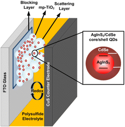 |
| | Fig. 1 Schematic diagram of an AgInS2/CdSe core/shell QDSSC. | |
2.1 Materials
Fluorine-doped tin oxide (FTO, 7 Ω per square) glass was purchased from Ruilong (Taiwan). TiO2 30 NR-D paste and TiO2 WER2-0 Titania Paste were obtained from GreatCell Solar. Silver nitrate (Ag(NO)3) and copper(II) sulfate pentahydrate (CuSO4·5H2O) were purchased from Honeywell Fluka. Sodium sulfide nonahydrate (Na2S·9H2O), selenium powder, and sodium thiosulfate anhydrous (Na2S2O3) were obtained from Thermo Fisher Scientific. Zinc acetate dihydrate (Zn(CH3COO)2·2H2O) and potassium chloride (KCl) were from JT Baker Chemical Company. Cadmium acetate (Cd(CH3COO)2·2H2O), indium chloride (In(Cl)3), and sodium borohydride (NBrH4) were from Alfa Aesar. Urea (CH4N2O) was from Sigma Aldrich. The sulfur powder was from Showa Chemical. All materials were used directly without any further purification.
2.2 Preparation of TiO2 electrodes
The TiO2 electrode was prepared using the following steps. First, a TiO2 blocking layer, 50–70 nm in thickness, was coated on the precleaned FTO glass by spin-coating 50 μl of a 0.247 M titanium(IV) isopropoxide solution. Then, a mesoporous TiO2 (mp-TiO2) layer with a thickness of 10–12 μm, particle size ∼30 nm, and 0.3 cm in diameter was coated on top of the blocking layer by doctor-blading TiO2 paste (Greatcell DSL 30NR-T), then heated at 120 °C for 5 min. Thirdly, a TiO2 scattering layer, particle size 350 nm, thickness ∼5 μm, and diameter 0.5 cm, was coated on top of the mp-TiO2 layer by doctor blading a prepared solution (Greatcell WER4-0). The prepared TiO2 electrode was finally annealed at 500 °C for 90 min.44
2.3 Preparation of AgInS2 core QDs
AgInS2 QDs were grown onto an mp-TiO2 electrode using a two-stage successive ionic layer adsorption and reaction (SILAR) method.45–48 First, binary Ag–S QDs seeds were grown onto an mp-TiO2 electrode. Second, binary In–S QD seeds were deposited on the Ag–S QD seeds. Post-annealing at an elevated temperature transformed the Ag–S/In–S double-layered structure to the AgInS2 phase. In detail, the mp-TiO2 electrode was first dipped into a 25 °C, 0.05 M Ag(NO)3 ethanol solution for 30 s, then rinsed using ethanol and dried on a hotplate at 40 °C. Then, the sample was immersed into a 25 °C, 0.1 M Na2S·9H2O methanol/DI water (1:1, v/v) solution for 120 s, rinsed with methanol, and dried on a hotplate at 40 °C. These two steps were denoted as one SILAR cycle of Ag–S. The number of cycles was fixed into two to obtain the suitable amount of Ag–S seeds. For the In–S seeds deposition, the Ag–S-coated TiO2 electrode was immersed into a 25 °C, 0.1 M In(Cl)3 ethanol solution for 120 s, rinsed with ethanol, and dried on the hotplate at 40 °C. Then, the sample was dipped into a 25 °C, 0.1 M Na2S·9H2O methanol/DI water (1:1, v/v) solution for 120 s and rinsed with methanol and dried on a hotplate at 40 °C. The two-dipping process was referred to as one SILAR cycle of In–S seeds. The number of cycles was fixed at seven to obtain the suitable amount of AgInS2 QDs. Finally, the sample was annealed under the nitrogen atmosphere at 300 °C for 30 min, yielding the AgInS2 core QDs.
2.4 Preparation of CdSe shell QDs
The CdSe shell was grown onto the AgInS2-coated mp-TiO2 electrode using the SILAR method. In detail, a Se precursor solution was prepared by dissolving 0.36 g of selenium powder into 125 ml of ethanol solution containing 0.3 g of NBrH4. The AgInS2-coated TiO2 electrode was dipped into a 0.1 M Cd(CH3COO)2·2H2O methanol solution for 60 s, rinsed with methanol, and dried on a hotplate at 40 °C. The sample was then immersed in the Se precursor solution for 90 s, rinsed using ethanol, and dried on a hotplate at 40 °C. This two-step dipping process was called one SILAR cycle of CdSe. The cycle was repeated six times to obtain the desired amount of CdSe shell QDs.
2.5 Preparation of a ZnSe passivation layer
The synthesized AgInS2/CdSe core/shell QDs were passivated with a ZnSe layer using the SILAR method to reduce carrier recombination. Briefly, the prepared sample was dipped into a 0.1 Zn(CH3COO)2·2H2O DI-water solution for 120 s, rinsed with DI-water, and dried on a hotplate at 40 °C. Then, the sample was immersed in the Se solution mentioned above for 90 s, rinsed with ethanol, and dried on a hotplate at 40 °C. This two-step process was repeated four times, forming a ZnSe passivation layer on the AgInS2/CdSe core/shell QDs.
2.6 Assembly of solar cells and characterization
The AgInS2/CdSe core/shell QDs were assembled into the liquid-junction QD-sensitized solar cell structure by sandwiching the prepared AgInS2/CdSe electrode with a CuS counter electrode using a parafilm spacer of thickness 190 μm. The CuS counter electrode was prepared using the chemical bath deposition method.47 In brief, three to six precleaned FTO glass was immersed horizontally in a 40 ml solution containing 1.564 g of CuSO4·5H2O, 3.968 g of Na2S2O3, and 0.969 g of CH4N2O, for 70 min on a hotplate at 55 °C, rinsed with DI-water and dried at 60 °C. The polysulfide electrolyte, consisting of 1 M Na2S, 2 M S, and 0.2 M KCl in methanol/water (7:3 by volume), was injected into the space between the TiO2 electrode and the CuS counter electrode before J–V measurements.
The photocurrent–voltage (J–V) characteristics were measured using a Keithley 2400 source meter under 100 mW cm−2 light illumination from a 150 W Xe lamp. A batch of three to six samples was measured parallel to ensure data consistency. A metal mask of the size 3 mm × 3 mm was used during measurements to avoid overestimated current densities. The X-ray diffractometer (XRD) patterns were obtained using a Bruker XRD D2 Phaser. Transmission electron microscopy (TEM) was conducted using JEOL JEM-2010. Energy dispersive spectroscopy (EDS) was analyzed using a JEOL JSM-6700F scanning electron microscope (SEM). Optical characteristics were obtained from a Hitachi U-2800A UV-vis spectrophotometer. External quantum efficiency (EQE) spectra were collected from an Acton monochromator with a 250 W tungsten halogen lamp source (without white-light biasing).
2.7 Electrochemical measurements
Cyclic voltammograms (CV) were retrieved from Bio-Logic SAS SP-150. The reference electrode employed in this study was an Ag/AgCl electrode, while the counter electrode utilized platinum (Pt). The working electrode was prepared through the following steps: (i) a mesoporous titanium dioxide (mp-TiO2) layer, possessing a thickness ranging from 18 to 20 μm, particle size of 30 nm, and dimensions of 1.2 × 1 cm, was deposited onto the blocking layer using the doctor-blading technique with TiO2 paste; (ii) the AgInS2 and CdSe quantum dots (QDs) were synthesized within the mp-TiO2 layer following established procedures. Electrochemical experiments were executed within a sample vial equipped with a specialized cap. The reference electrode was strategically positioned between the working electrode, connected to the equipment via an electric clamp, and the Pt counter electrode. The measurement comprised several cycles within a potential range spanning from −1.0 to 2.0 V, employing a scan rate of 100 mV s−1. A 0.1 M KCl solution served as the supporting electrolyte during the electrochemical analysis. In a setup where AgInS2 and CdSe QDs are grown on mp-TiO2 nanoparticles, the cyclic voltammetry (CV) signal predominantly reflects the redox reactions at the electrode surface. Despite TiO2 being present, the electrochemical behavior of AgInS2 and CdSe QDs dominates the observed signal. Utilizing the anodic and cathodic peaks of AgInS2 and CdSe QDs grown onto mp-TiO2 nanoparticles is a reasonable approach to estimating the position of the valence band (VB) and conduction band (CB) position. Therefore, in this study, the valence band level (EVB) and conduction band level (ECB) positions were estimated by analyzing oxidation and reduction peak potentials.49 After completing each round of experiments, the potentials were adjusted in reference to the normal hydrogen electrode (NHE) and the potential of the Ag/AgCl electrode. The electrochemical bandgap was calculated as the difference between these peak potentials.50
3 Results and discussion
3.1 Structural analysis
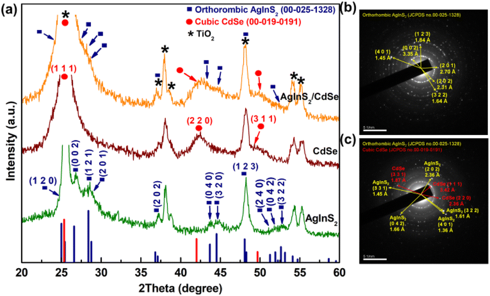
The crystalline structures of the synthesized QDs were analyzed using XRD. As depicted in Fig. 2(a), all peaks from AgInS2 QDs match correctly with the orthorhombic AgInS2 crystal structure (JCPDS No. 00-025-1328) without impurities; some peaks overlap with the TiO2 peaks (JCPDS No. 00-002-0387), namely the (1 2 0) peak at 24.99°, (2 0 2) at 37.12°, and (1 2 3) at 48.05°, while the AgInS2 peaks of (0 0 2), (1 2 1), (2 0 1), (0 4 0), (3 2 0), (2 4 0), (0 4 2), and (3 2 2) are well separated with the TiO2 background. The CdSe QDs show the cubic structure (JCPDS No. 00-019-0191), consisting of three prominent peaks: (1 1 1) at 25.35°, (2 2 0) at 42.01°, and (3 1 1) at 49.67°. In the XRD pattern of AgInS2/CdSe core/shell QDs, some AgInS2 peaks, such as (0 0 2) at 26.58°, (1 2 1) at 28.38°, (2 0 1) at 28.75°, (0 4 0) at 43.69°, and (3 2 0) at 44.53°, become less apparent due to partial overlap with the CdSe peaks of (1 1 1) at 25.35°, and (2 2 0) at 42.01°. The deconvoluted analysis (ESI Fig. S1†) shows that the patterns contain all corresponding peaks of AgInS2 and CdSe, indicating the successful formation of AgInS2 and CdSe crystal structures. The SAED peaks of AgInS2 QDs (Fig. 2(b)) and AgInS2/CdSe QDs (Fig. 2(c)) are in agreement with the XRD analysis.
 |
| | Fig. 2 (a) XRD pattern of AgInS2 QDs, CdSe QDs, and AgInS2/CdSe core/shell QDs, (b) selected area (electron) diffraction (SAED) of AgInS2 QDs, and (c) SAED of AgInS2/CdSe core/shell QDs. | |
In this study, lattice constants of the synthesized QDs were determined by analyzing the XRD peak shifts of AgInS2 and CdSe concerning the standard position within the XRD pattern of related materials. These measurements were compared with the lattice parameters of ideal single crystals of AgInS2 and CdSe obtained from a reputable XRD database. The findings, showcased in Table 1, present the calculated results of these comparisons.
Table 1 Lattice constant and volume of the cell of ideal single crystal AgInS2 (JCPDS No. 00-025-1328), synthesized AgInS2, ideal single crystal CdSe (JCPDS No. 00-019-0191), and synthesized CdSe
| Sample |
Lattice constant (Å) |
Volume of cell (pm3) |
|
a
|
b
|
c
|
| Ideal single crystal AgInS2 (JCPDS No. 00-025-1328) |
7.001 |
8.278 |
6.698 |
388.18 × 10⁶ |
| Synthesized AgInS2 QDs |
6.989 |
8.204 |
6.682 |
383.13 × 10⁶ |
| Ideal single crystal CdSe (JCPDS No. 00-019-0191) |
6.077 |
6.077 |
6.077 |
224.42 × 10⁶ |
| Synthesized CdSe QDs |
6.008 |
6.008 |
6.008 |
216.86 × 10⁶ |
Table 1 shows that the determined lattice constants of the synthesized QDs differ from the database references for ideal crystal structures of AgInS2 (JCPDS No. 00-025-1328) and CdSe (JCPDS No. 00-019-0191), implying that the synthesized QDs might undergo the lattice distortion phenomenon.51 Furthermore, Table 2 includes calculations of the strain resulting from varied d-spacings obtained using the Bragg equation and eqn (1) compared to the ideal d-spacings listed in the same XRD database.
| | 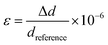 | (1) |
where
ε is the microstrain, Δ
d is the difference in
d-spacing, and
dreference is the reference
d-spacing.
Table 2 Calculated microstrain resulting from the difference between the measured d-spacing and the ideal single crystal d-spacing
| Sample |
Miller indices |
Measured d-spacing (Å) |
Ideal d-spacing (Å) |
Calculated microstrain (× 10−6) |
| AgInS2 |
002 |
3.341 |
3.350 |
−2.687 |
| 040 |
2.051 |
2.070 |
−9.178 |
| 320 |
2.026 |
2.033 |
−3.445 |
| CdSe |
220 |
2.124 |
2.149 |
−11.633 |
Table 2 reveals that all calculated microstrain values exhibit a negative sign, indicating compressive strain and suggesting compression or contraction within the crystal lattice. Specifically, CdSe QDs demonstrate a larger microstrain value than AgInS2 QDs. This difference can be attributed to the growth process utilized for CdSe in this study, which omitted the annealing step after SILAR. The absence of annealing can cause various effects, including incomplete relaxation of internal stresses, limited structural reorganization, and accumulation of defects, resulting in larger strain.
The preceding outcomes suggest that these distortions and strains emerged during the QD growth process on TiO2 using the SILAR method. Several contributing factors may have led to these lattice distortions and strains, such as (i) SILAR involves sequential adsorption of precursor ions or molecules followed by reaction or deposition, leading to nanoscale structure growth. Irregularities in nucleation, growth kinetics, or layer thickness variations contribute to lattice strain; (ii) interface mismatches between layers or substrate in SILAR-deposited materials introduce strain due to differences in lattice parameters or surface energies; (iii) epitaxial or quasi-epitaxial growth in SILAR may cause strain if deposited layers deviate from substrate orientation; (iv) surface defects, variations in layer quality, or surface states influence material strain; (v) the deposition process induces mechanical stress from factors like island growth or lattice mismatch, (vi) quantum dot boundary defects with differing orientations can cause lattice distortion. Identifying specific strain-inducing factors often necessitates detailed analysis using techniques such as transmission electron microscopy (TEM). The advanced characterization of the lattice mismatch using high-resolution transmission electron microscopy (HR-TEM) was carried out to enhance the analysis, as detailed in the subsequent explanation. While the above analysis requires careful consideration of instrumental effects influencing discrepancies between the synthesized QDs and the ideal single crystal of related materials, combining XRD pattern analysis with TEM findings enables the identification of defects in AgInS2 and CdSe QDs grown on TiO2 nanoparticle surfaces. Lattice distortion, strain, and lattice mismatch contribute to the formation and propagation of defects in the crystal lattice. These defects may account for unfavorable charge carrier recombination, a factor further detailed in the subsequent photovoltaic performance analysis.
3.2 Scanning electron microscopy (SEM) and energy dispersive spectroscopy (EDS) analysis
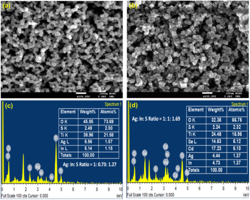
The surface morphology of TiO2/AgInS2 core and TiO2/AgInS2/CdSe core/shell QDs was analyzed using SEM, as depicted in Fig. 3(a) and (b). The TiO2/AgInS2 sample shows a porous structure. The AgInS2/CdSe QDs exhibit a slightly larger particle size. The elemental composition of the QDs was analyzed using SEM-EDS. As shown in Fig. 3(c), the atomic percentage of Ag, In, and S were 1.57%, 1.15%, and 2.00%, respectively, yielding an elemental ratio of 1:0.73:1.27, which can be approximated to a 1:1:2 ratio; this result is in good accordance with the XRD pattern. In the AgInS2/CdSe core/shell QDs (Fig. 3(d)), the Cd and Se atomic percentages were 5.10% and 6.12%, giving an approximate ratio of 1:1 for Cd:Se. Meanwhile, the atomic percentage of Ag, In, and S slightly changed to 1.37%, 1.37%, and 2.32%, respectively, maintaining the 1:1:2 ratio for Ag:In:S.
 |
| | Fig. 3 Top view of SEM pictures of (a) TiO2/AgInS2 and (b) TiO2/AgInS2/CdSe core/shell with a magnification of 100000 times; EDS spectra of (c) TiO2/AgInS2 and (d) TiO2/AgInS2/CdSe core/shell. | |
3.3 Transmission electron microscopy (TEM) analysis
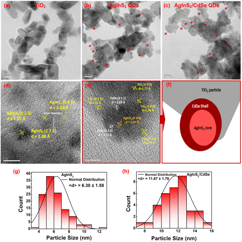
The morphology of the synthesized QDs was investigated using TEM, as shown in Fig. 4. The bare mp-TiO2 nanoparticles have a hexagonal shape with round edges and an average particle size of 30 nm (Fig. 4(a)). The AgInS2 QDs, denoted with red arrows in Fig. 4(b), were distributed randomly on TiO2 nanoparticles. The AgInS2 particle sizes were in the range of 4–12 nm with an average size of 6.3 nm (the normal distribution of particle sizes is depicted in Fig. 4(g)). Fig. 4(d) depicts the lattice fringes of three individual AgInS2 QDs with different planes. The d-spacings of the lattice fringes for the (1 2 3) plane were 0.185 nm and 0.188 nm for two individual QDs, showing reasonable consistency. The lattice fringes with the (0 4 0) plane have a d-spacing of 0.208 nm. These results agree with the orthorhombic AgInS2 crystal structure (JCPDS No. 00-025-1328). From Fig. 4(d), it is evident that two neighboring QDs possess different orientations, resulting in a calculated lattice mismatch of 9.26% and a detected grain boundary. The mismatch between their lattices leads to strain accumulation at the interface. This accumulated strain, aiming for relief, instigates the emergence of defects or irregularities near the boundary. Additionally, the lattice distortion caused by this mismatch induces defect formation to accommodate the strain. These accumulated defects may contribute to the development of specific structural anomalies near the boundary. These findings suggest the existence of such imperfections within the AgInS2 QDs grown on TiO2 nanoparticles. The subsequent section analyzing photovoltaic performance further explores how these imperfections impact the overall efficiency of the photovoltaic system.
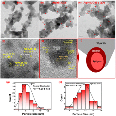 |
| | Fig. 4 TEM images of (a) mp-TiO2 nanoparticles, (b) AgInS2 QDs grown onto mp-TiO2 nanoparticles (the red arrows display the AgInS2 QDs), (c) AgInS2/CdSe QDs grown onto mp-TiO2 nanoparticles (the red arrows display the AgInS2/CdSe QDs), (d) lattice fringes of AgInS2 QDs, (e) lattice fringes of AgInS2/CdSe core/shell QDs (the red arrow indicates the diagram shown in (f)), (f) diagram that shows the boundary of the TiO2, AgInS2, and CdSe QD images shown in (e), (g) distribution of particle size of AgInS2, and (h) distribution of particle size of AgInS2/CdSe. | |
The formation of AgInS2/CdSe core/shell QDs enlarged the overall particle sizes, as given in Fig. 4(c); the AgInS2/CdSe core/shell QDs were distributed densely on the mp-TiO2; the particle sizes in the range of 7–15 nm with an average particle size of 11.7 nm (Fig. 4(h) depicts the normal distribution of the particle size). As illustrated in Fig. 4(e), the AgInS2/CdSe core/shell QD is grown onto mp-TiO2, which has three different planes: (2 0 0), (2 2 0), and (3 1 2). The CdSe QD with the plane of (3 1 1) is attached to the mp-TiO2 ((2 0 0) plane) and covers the AgInS2 core QD with the plane of (0 4 0), while the CdSe plane of (2 2 0) is adhered with another side of AgInS2 core QD ((0 4 0) plane). All the corresponding lattice fringes agree with the crystal structures of each material. Fig. 4(f) illustrates a schematic diagram that shows the boundary of the respective CdSe QD, AgInS2 QD, and a TiO2 nanoparticle shown in Fig. 4(e). As seen, the AgInS2 QD is surrounded by the CdSe QD. Meanwhile, the CdSe QD is attached to the TiO2 nanoparticle. The diagram further elucidates the formation of the core/shell QD structure. Based on the observations in Fig. 4(e), the CdSe shell manifests diverse orientations, resulting in a lattice mismatch of 13.27%. Notably, the calculated lattice mismatch between the CdSe shell and TiO2 nanoparticles varies significantly, ranging from 36.02% to 45.02%, depending on the nanoparticle orientation. However, the lattice mismatches between the AgInS2 core and the CdSe shell are comparatively lower at 6.64% and 7.65%. Essentially, the strain accumulation primarily responsible for inducing defects at the interface predominantly stems from the lattice mismatch between the CdSe shell and TiO2 nanoparticles. These results align with the XRD pattern analysis related to the strain analysis.
3.4 Optical spectra analysis
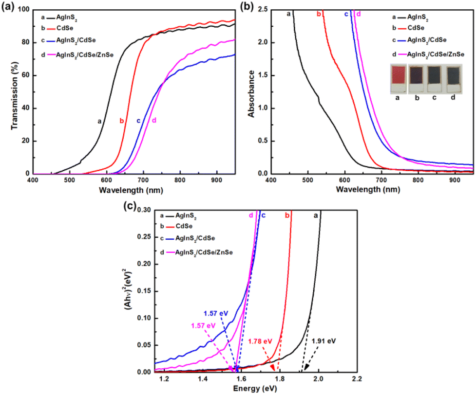
Fig. 5 compares the optical spectra of AgInS2, CdSe, and AgInS2/CdSe QDs. The transmission spectra T(λ) of each sample in Fig. 5(a) were measured as IQDs/ITiO2, where IQDs and ITiO2 are the light intensity passing through TiO2/QDs sample and TiO2 sample, respectively. The transmission spectra shifted to the longer wavelength region in the order of AgInS2, CdSe, and AgInS2/CdSe core/shell, indicating that the bandgap decreases with the order of AgInS2, CdSe, and AgInS2/CdSe core/shell. The addition of the ZnSe passivation layer appears to exert negligible influence on the optical spectra, as depicted in Fig. 5(a). Fig. 5(b) shows the absorbance spectra A(λ) = −log10T(λ). The AgInS2/CdSe core/shell had the largest absorbance value at a given wavelength, CdSe the second, and AgInS2 the smallest. For example, at λ = 700 nm, A = 0.504, 0.114, and 0.086 for AgInS2/CdSe, CdSe, and AgInS2, respectively. Fig. 5(c) shows the Tauc plots of the samples. The optical energy bandgap (Eg,op) was estimated by finding the intercept of the extrapolated line to the x-axis. The Tauc plots yielded the Eg of 1.91 eV (AgInS2), 1.78 eV (CdSe), and 1.57 eV (AgInS2/CdSe), respectively. The 1.91 eV of AgInS2 is consistent with the bandgap of 1.98 eV for orthorhombic AgInS2.37,38 The 1.78 eV of CdSe also agrees with the reported CdSe bandgap.52–54 Intriguingly, the core/shell QDs had an Eg of 1.57 eV, lower than the constituent core AgInS2 (1.91 eV) and CdSe shell (1.78 eV). Two possible explanations are: (i) the core/shell QDs were synthesized using a number of SILAR cycles larger than the core and shell. As reported by Robinovich and Hodes, the Eg of QD samples prepared by SILAR would decrease with an increasing number of SILAR cycles.55 The lower Eg of the core/shell QDs could be a consequence of the larger number of SILAR cycles used, and (ii) the type-II core/shell structure induces a narrow effective bandgap owing to the presence of the exciplex state. This will be explained in detail in the section on cyclic voltammetry below. The ZnSe passivation layer has minimal impact, with the energy bandgap remaining approximately consistent with that of the AgInS2/CdSe core–shell QDs at 1.57 eV.
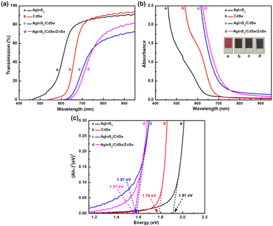 |
| | Fig. 5 Optical spectra of AgInS2, CdSe, AgInS2/CdSe: (a) transmission spectra T(λ), (b) absorbance A(λ), and (c) Tauc plot (Ahυ)2vs. hυ. | |
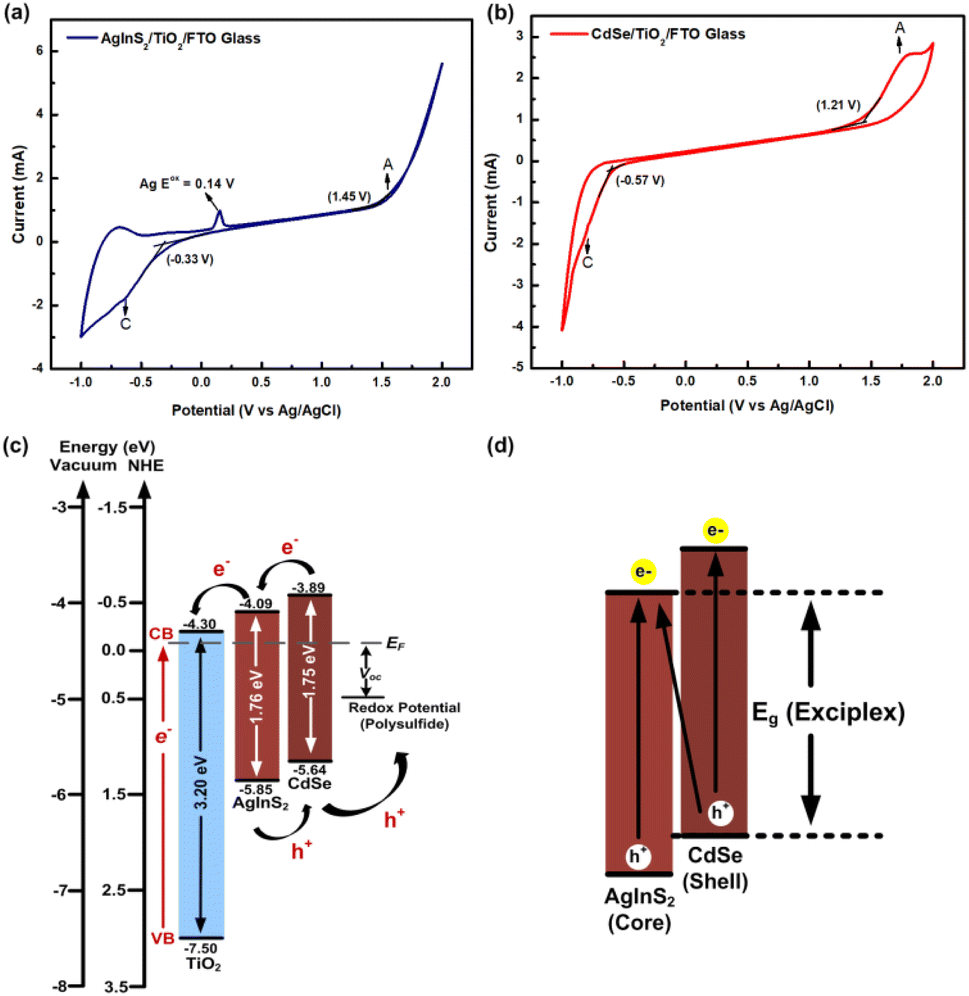
3.5 Cyclic voltammetry analysis
The determination of the core/shell type of AgInS2/CdSe QDs relies significantly on the positions of the valence band level (EVB) and conduction band level (ECB) of AgInS2 and CdSe QDs grown onto TiO2 nanoparticles. The estimation of band alignment was achieved through CV measurements, as exemplified in Fig. 6. In Fig. 6(a) and (b), during the potential scan from 0 V to a more positive value, an anodic peak (A) emerges, and conversely, upon reversing the cycle, a cathodic peak (C) is observed. These anodic and cathodic peaks are attributed to the electron transfer between the QDs and the working electrode through the EVB and ECB, respectively. Consequently, the EVB and ECB were calculated from the onset of anodic (A) and cathodic (C) peaks of the QDs. The onset of anodic peak (Eoxonset) was calculated by determining the intersection of two tangents drawn at the point where the oxidation current begins to rise and the background current in the cyclic voltammograms. Similarly, the onset of the cathodic peak (Eredonset) was computed by identifying the point where the reduction current starts to increase and determining the intersection of two tangents drawn at that position and the background current in the cyclic voltammograms; the numerical values enclosed in brackets within Fig. 6(a) and (b) indicate the onset potential. The energy levels were calculated using formulas (2) and (3).50| | | ECB = −e(Eredonset + 4.4) eV | (2) |
| | | EVB = −e(Eoxonset + 4.4) eV | (3) |
 |
| | Fig. 6 Cyclic voltammetry (CV) curves of (a) AgInS2 QDs, (b) CdSe QDs grown onto TiO2 nanoparticles; the letters A and C in the figures express the anodic and cathodic peak, respectively; the number in the bracket shows the onset potential, (c) band alignment of AgInS2 and CdSe QDs determined from CV curves, and (d) schematic diagram of AgInS2/CdSe type-II core/shell band alignment with an energy bandgap from exciplex state. | |
Based on Fig. 6(a), the AgInS2 QDs showed the oxidation peak of Ag at 0.14 V; the EVB and ECB of AgInS2 QDs are −5.85 eV and −4.09 eV, respectively, resulting in a bandgap (Eg,CV) of 1.76 eV. The bandgap derived from CV measurements may not invariably align with the optical bandgap, as it hinges on the specific semiconductor material under investigation. The observed peak shift in CV could potentially arise from trapping sites enabling numerous electrons and holes to engage in the reaction. This distinction underscores that the CV-derived bandgap might not be directly synonymous with the optical bandgap due to the influence of trapping mechanisms within the semiconductor material.56 The outcomes observed in this study align with prior research investigating the energy bandgap using CV. Mohan and Renuga documented the EVB and ECB of AgInS2 nanocrystals as −5.61 eV and −3.87 eV, respectively.57 Similarly, Jagadeeswararao et al. reported the EVB and ECB of AgInS2 nanocrystals as −6.0 eV and −3.94 eV.58 The CdSe QDs in Fig. 6(b) yielded respective EVB of −5.64 eV and ECB of −3.89 eV, resulting in an Eg,CV of 1.75 eV. These results are comparable with many other studies measuring the electrochemical bandgap of CdSe QDs. For instance, the reported values for the EVB and ECB of CdSe QDs were −5.86 eV and −3.66 eV,56 respectively. Additionally, another study documented the ECB of CdSe QDs as −3.71 eV.59 Furthermore, a range of values was observed for the EVB and ECB of CdSe QDs, varying in size from 1.9 nm to 3.4 nm. These values spanned from −5.68 eV and −2.83 eV to −3.26 eV and −5.47 eV, respectively.60 It is noteworthy to consider potential experimental uncertainties and methodological variations between measurement techniques when comparing these results. Considering this comparative analysis, the inferred EVB and ECB values in our study appear logically justifiable, potentially indicating a core–shell type configuration. Consequently, based on this analysis, it is evident that the EVB and ECB levels of CdSe QDs are higher compared to the corresponding levels of AgInS2 QDs, indicating the formation of a type-II core/shell structure, as depicted in Fig. 6(c). In this type-II core/shell QD structure, the electrons are confined to the core while the holes are confined to the shell, leading to effective charge separation.54 This structure produces an exciplex state, which offers an additional route (indirect interfacial transition) to improve spectral response, consequently lowering the effective bandgap (Eg (Exciplex)), as shown in Fig. 6(d).28
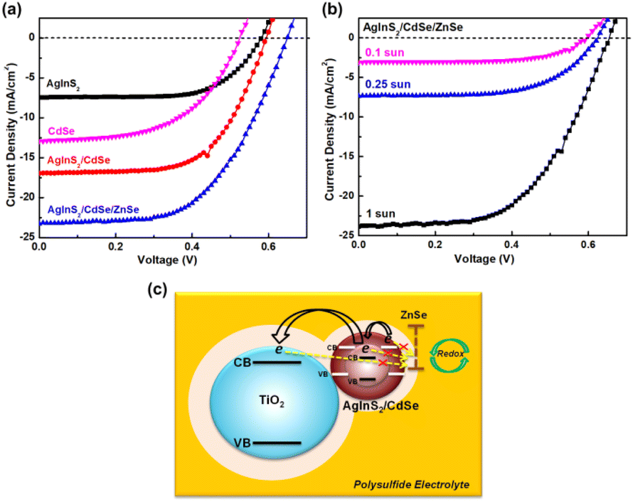
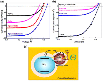
3.6 Photovoltaic performance
The photovoltaic characteristics of AgInS2/CdSe core/shell QDSSCs were measured under 1 sun (100 mW cm−2) light intensity. Single-layered AgInS2 core and CdSe shell QDSSCs were studied simultaneously for comparison. Table 3 lists the photovoltaic parameters, including the short-circuit current density (Jsc), open-circuit voltage (Voc), fill factor (FF), and power conversion efficiency (PCE). Fig. 7(a) depicts the J–V curves for each sample. The single-layered AgInS2 core QDSSC achieved an average PCE of 3.04% (Jsc = 7.72 mA cm−2, Voc = 0.66 V, FF = 60.0%). The PCE of 3.04% achieved in this work is slightly higher than the best PCE of 2.91% for AgInS2 QDSSCs reported recently.41 Building upon the theory mentioned in the literature,61 the maximum attainable Jsc for an ideal solar absorber material, with an absorption onset at a wavelength λ of 713 nm (as per EQE spectra), is estimated to be 20.4 mA cm−2. Nevertheless, the generated Jsc in this study amounts to only 7.72 mA cm−2. This outcome could be elucidated by considering the XRD pattern and TEM analysis, which suggest that the reduced Jsc observed in AgInS2 QDSSCs might stem from increased carrier recombination due to defects linked to imperfections within the AgInS2 QDs grown on TiO2. Meanwhile, the single-layered CdSe shell QDSSCs achieved an average PCE of 3.67% (Jsc = 12.9 mA cm−2, Voc = 0.52 V, FF = 55.1%). The low PCE observed in CdSe shell QDSSCs can also be ascribed to carrier recombination due to imperfections within the CdSe QDs cultivated on TiO2. Nevertheless, the AgInS2/CdSe core/shell QDSSCs (sample no.5) achieved an average PCE of 6.49% (Jsc = 16.95 mA cm−2, Voc = 0.59 V, FF = 64.9%), a significant increase that nearly doubles the PCEs of the single-layered core and shell QDSSCs. Higher Jsc is assigned to the extension of the light-absorption range (explained in the optical spectra) and the multiplication of electron injections from the core or the shell. However, the Voc decreases by 11%, which can be explained based on the standard diode eqn (4)| | 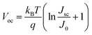 | (4) |
where T is the temperature, kB is the Boltzmann constant, q is the electron charge, and J0 is the saturation current density. The J0 depends on the recombination in the solar cells; therefore, based on eqn (4), lower Voc is ascribed to a higher amount of recombination in the cells. As mentioned in the XRD pattern and TEM analysis, the CdSe generated through the SILAR method without annealing harbors defects arising from lattice mismatches and crystal imperfections, subsequently functioning as recombination centers. The AgInS2/CdSe core/shell QDSSCs were then coated with a ZnSe passivation layer to suppress carrier recombination. The ZnSe-coated AgInS2/CdSe/ZnSe QDSSC (sample no. 7) yielded an average PCE of 8.39% (Jsc = 23.28 mA cm−2, Voc = 0.64 V, FF = 56.0%), a 29% improvement over that of the uncoated core/shell cell (sample no. 5). As depicted in Fig. 7(c), the presence of the ZnSe passivation layer effectively hinders the recombination of electrons originating from the conduction bands of CdSe, AgInS2, or TiO2 with Sn2− in the electrolyte. This preventive effect contributes to an enhancement in the overall performance of the solar cells. The PCE of 8.39% achieved here is higher than the best PCEs among all type-II core/shell QDSSCs reported to date, such as ZnTe/CdSe (7.17%) and Dy-doped CdTe/CdS (8.26%).31,34
Table 3 Photovoltaic performance of single-layered AgInS2, CdSe and core/shell AgInS2/CdSe QDSSCs
| No. |
Sample |
J
sc (mA cm−2) |
V
oc (V) |
FF (%) |
PCE (%) |
|
Average value from three cells.
Champion cell.
|
| 1 |
AgInS2a |
7.72 ± 0.75 |
0.66 ± 0.02 |
60.0 ± 0.3 |
3.04 ± 0.29 |
| 2 |
AgInS2b |
8.58 |
0.66 |
59.7 |
3.38 |
| 3 |
CdSea |
12.9 ± 1.18 |
0.52 ± 0.00 |
55.1 ± 6.4 |
3.67 ± 0.08 |
| 4 |
CdSeb |
11.55 |
0.52 |
62.42 |
3.75 |
| 5 |
AgInS2/CdSea |
16.95 ± 0.43 |
0.59 ± 0.02 |
64.9 ± 1.6 |
6.49 ± 0.04 |
| 6 |
AgInS2/CdSeb |
16.73 |
0.61 |
63.9 |
6.53 |
| 7 |
AgInS2/CdSe/ZnSea |
23.28 ± 1.09 |
0.64 ± 0.02 |
56.0 ± 0.7 |
8.39 ± 0.18 |
| 8 |
AgInS2/CdSe/ZnSeb |
23.85 |
0.65 |
55.2 |
8.57 |
 |
| | Fig. 7 (a) J–V curves of AgInS2, CdSe, AgInS2/CdSe core/shell, and AgInS2/CdSe core/shell/ZnSe under 1 sun, (b) J–V curves of AgInS2/CdSe core/shell/ZnSe under different sun intensities, and (c) schematic diagram of electron transfer from an AgInS2/CdSe core/shell QD into a TiO2 nanoparticle with a ZnSe passivation layer. | |
Semiconductor nanoparticles prepared by SILAR contain a large number of defects due to the low-temperature synthesis, as evident from the XRD pattern and TEM analysis. These defects act as recombination centers. When illuminated under 1 sun, representing a higher photon influx, there is an increased generation of electron–hole pairs. However, a substantial portion of these pairs undergo recombination. Consequently, scrutinizing the current–voltage (J–V) curves at low light intensities proves valuable in alleviating the adverse effects of recombination from these defects, thereby improving the overall performance. Fig. 7(b) shows the I–V curves of the best AgInS2/CdSe core/shell QDSSCs under various reduced sun intensities. Table 4 lists the photovoltaic parameters. The PCE enhanced from 8.57% (1 sun) to 11.15% (0.25 sun) and further to 11.75% (0.1 sun), a 36.5% improvement over the 1 sun data. The enhanced PCE arose from both Jsc and FF, Jsc boosted from 23.85 mA cm−2 (1 sun) to 3.07 mA cm−2 (0.1 sun), which could be normalized to 30.7 mA cm−2 (1 sun). In addition, the FF increased from 55.26% (1 sun) to 64.80 (0.1 sun). The enhanced Jsc and FF indicate improved photocarrier collection. The improvement can be explained in terms of the multiple trapping model for carrier recombination proposed by Tachiya and Seki.62 The model assumes carriers could be trapped and de-trapped repeatedly from trap surface sites. The theory predicts a sublinear Jscvs. light intensity I0 power law: Jsc ∝ I0α (α < 1). Analysis of the Jscvs. I0 data in Table 3 yielded α = 0.89 (ESI Fig. S2†), consistent with the multiple trapping model. Similar sublinear relations ne ∝ I00.6 and ne ∝ I00.45 have been reported in dye-sensitized solar cells,63,64 where ne is the electron density. In addition, the power laws of Jsc ∝ I00.72 and Jsc ∝ I00.52 have been reported in Pb5Sb8S17 and NaSbS2 QDSSCs, respectively.65,66 According to the multiple trapping model, Jsc decreases at a lower rate than that of the light intensity I0 because α < 1. For example, if α = 0.5 and the light intensity I0 decreases by four times, then Jsc decreases only by two times. The number of photocarriers is reduced under low light intensities, which reduces the photocarrier trapping/de-trapping activity and the occurrence of carrier recombination, leading to more efficient carrier collection and higher efficiency.
Table 4 Photovoltaic performance of AgInS2/CdSe/ZnSe core/shell QDSSCs under different sun intensities
| Sun intensity |
J
sc (mA cm−2) |
V
oc (V) |
FF (%) |
PCE (%) |
| 1 sun |
23.85 |
0.65 |
55.26 |
8.57 |
| 0.25 sun |
7.34 |
0.62 |
61.27 |
11.15 |
| 0.10 sun |
3.07 |
0.59 |
64.80 |
11.75 |
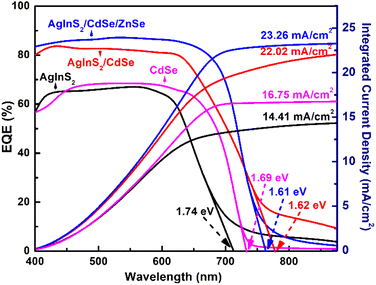
3.7 External quantum efficiency (EQE)
EQE is essential for evaluating the efficiency of photoelectron generation. Fig. 8 depicts the EQE spectra and EQE-deduced integrated current density of three QDSSCs: AgInS2, CdSe, and AgInS2/CdSe/ZnSe. The AgInS2 core QDSSCs covered the EQE spectra range of 350–700 nm with a nearly constant EQE value of ∼65% over the range of 350–600 nm. The EQE onset, corresponding to the bandgap Eg,pv, of the AgInS2 QDSSCs, was 712 nm (Eg,pv = 1.74 eV). The CdSe shell QDSSCs covered the spectra range of 350–720 nm with a nearly constant EQE value of ∼68% over the range of 400–650 nm. The EQE onset was 733 nm (Eg,pv = 1.69 eV). Moreover, the CdSe shell exhibited significantly higher EQE values than that of the AgInS2 core over the long-wavelength region of 600–700 nm. For the AgInS2/CdSe core/shell QDSSCs, the EQE spectra exhibited a slightly broader range of 350–725 nm with significantly higher EQE values of 80–84% over the spectral range of 350–625 nm. Meanwhile, the EQE onset decreased slightly to Eg,pv = 1.62 eV (765 nm). The addition of the ZnSe passivation layer improved the EQE response and reduced the bandgap tails, particularly evident beyond 800 nm, accompanied by substantially elevated EQE values ranging from 82% to 85% over the interval of 350–700 nm. Concurrently, the EQE onset is similar to the AgInS2/CdSe core/shell QDSSCs with Eg,pv = 1.61 eV (770 nm). Two notable results of the EQE spectra are: (a) the core/shell QDSSCs yielded higher EQE values (84%) than that of the core and shell (∼65%), (b) the core/shell QDSSCs exhibited slightly broader spectral range (up to 765 nm) compared to the core (710 nm) and CdSe shell (730 nm). Lastly, some weak EQE signals (EQE < 15%) appeared in the long-wavelength region of λ > 800 nm. These weak EQE signals are attributed to the localized states within the bandgap that arise from defects in QDs, similar to a semiconductor's Urbach tail.
 |
| | Fig. 8 EQE spectra of AgInS2, CdSe, and AgInS2/CdSe/ZnSe QDSSCs and their integrated current density. | |
The photocurrent generated by a solar cell was calculated by integrating the area under an EQE curve. The integrated Jscs were 14.41, 16.75, and 23.26 mA cm−2 for the AgInS2 core, CdSe shell, and AgInS2/CdSe core/shell, respectively, as shown in the right axis of Fig. 8. The integrated Jsc of 23.26 mA cm−2 for the AgInS2/CdSe core/shell is consistent with the Jsc of 23.28 mA cm−2 obtained from I–V measurements shown in Table 2.
The AgInS2/CdSe core/shell solar cell exhibited a distinctly higher PCE (8.39%, 1 sun) than that of both the single-layered AgInS2 core (3.04%) and the CdSe shell cells (3.67%). As Table 1 indicates, the improved PCE arises mainly from Jsc, which is 23.28 mA cm−2 for AgInS2/CdSe core/shell, compared to 7.72 mA cm−2 (AgInS2) and 12.9 mA cm−2 (CdSe). The significantly larger improvement in Jsc is attributed to five features of the core/shell structure: (1) spatial separation of electron and holes: in the AgInS2/CdSe core/shell QD, the photogenerated electrons are located in the CB of AgInS2 core while holes in the VB of CdSe shell. The spatially separated electrons and holes reduce the overlap of their wavefunctions and, hence, carrier recombination, (2) shell layer as an energy barrier for recombination: the CB of the CdSe shell is higher than the CB of AgInS2 core. The CdSe CB, acting as an energy barrier, prevents photoelectrons in the CB of AgInS2 from recombining with holes in the electrolyte, (3) cascade energy structure: the CB and VB of AgInS2/CdSe core/shell form a cascade energy structure, as shown in Fig. 6(c). Electrons can jump from the CB of the CdSe shell to the CB of the AgInS2 core, then into the CB of the TiO2 electron transport layer. Similarly, holes can jump from the VB of the AgInS2 core and then to the VB of CdSe. Cascade energy structures can facilitate the electron injection and collection in a solar cell, as has been shown in many types of solar cells such as Zn–Cu–In–S QDs67–70 and dye-sensitized solar cells,71 (4) broader absorption spectrum: the AgInS2/CdSe core/shell QD has an absorption onset of 765 nm (1.62 eV), which is slightly broader than the AgInS2 core (712 nm, 1.74 eV) and CdSe shell (733 nm, 1.69 eV), as revealed in the EQE spectra. According to the literature,61 the maximum Jsc for a perfect solar absorber material (i.e., EQE = 100%) with an absorption onset of wavelength λ is ∼24.0 mA cm−2 for λ = 765 nm, 21.0 mA cm−2 for λ = 733 nm and 19.5 mA cm−2 for λ = 712 nm. The broader absorption range of the core/shell can produce a Jsc 15% more than that of the core and shell, (5) the decrease in the effective bandgap resulting from the exciplex state represents a distinctive characteristic of the type-II core/shell structure. As illustrated in the band energy diagram shown in Fig. 6(d), the energy bandgap originating from the exciplex state is lower than that of both AgInS2 (1.76 eV) and CdSe (1.75 eV), thereby broadening the absorption spectrum of the QDs. In other words, the exciplex state may have the potential for an indirect interfacial transition. To summarize, the reduced carrier recombination through spatially separated carriers, improved electron injection through the cascade energy structure, better light harvesting through the broader absorption band, and a possible indirect interfacial transition lead to a Jsc in the core/shell cell twice larger than that of the core and shell.
4 Conclusions
We demonstrated type-II AgInS2/CdSe core/shell QDSSCs prepared on mesoporous TiO2 using SILAR. The AgInS2/CdSe core/shell QDSSCs achieve a PCE of 8.39% under 1 sun and 11.75% under 0.1 sun. The PCE and Jsc of the core/shell cells are nearly three times larger than those of the single-layered AgInS2 cells. The PCE of the AgInS2/CdSe cells ranks as one of the top efficiency among all type-II core/shell QDSSCs reported. The cascade energy structure and spatial separation of electron/hole are the primary reasons that lead to the improved performance in the AgInS2/CdSe core/shell structure.
Author contributions
Siti Utari Rahayu: conceptualization, data curation, formal analysis, investigation, methodology, validation, visualization, and writing – original draft. Yu-Rou Wang: data curation, investigation. Jen-Bin Shi: formal analysis. Ming-Way Lee: conceptualization, formal analysis, funding acquisition, methodology, project administration, resources, supervision, validation, and writing – review & editing.
Conflicts of interest
There are no conflicts to declare.
Acknowledgements
The authors are grateful for the financial support from the Ministry of Science and Technology (MOST) in Taiwan under grant no. MOST 111-2112-M-005-017. We are grateful to Prof. Ja-an Annie Ho and Dr Thirupatthi Murugan of the Department of Biochemical Science and Technology at National Taiwan University for their support and discussions on the CV measurements.
References
- S. Gorer and G. Hodes, J. Phys. Chem., 1994, 98, 5338–5346 CrossRef CAS.
- I. Moreels, K. Lambert, D. De Muynck, F. Vanhaecke, D. Poelman, J. C. Martins, G. Allan and Z. Hens, Chem. Mater., 2007, 19, 6101–6106 CrossRef CAS.
- R. D. Schaller and V. I. Klimov, Phys. Rev. Lett., 2004, 92, 186601 CrossRef CAS PubMed.
-
P. Sudhagar, E. J. Juárez-Pérez, Y. S. Kang and I. Mora-Seró, in Low-cost Nanomaterials, ed. Z. Lin and J. Wang, Springer London, London, 2014, pp. 89–136 Search PubMed.
- G. Larramona, C. Choné, A. Jacob, D. Sakakura, B. Delatouche, D. Péré, X. Cieren, M. Nagino and R. Bayón, Chem. Mater., 2006, 18, 1688–1696 CrossRef CAS.
- N. Guijarro, T. Lana-Villarreal, I. Mora-Seró, J. Bisquert and R. Gómez, J. Phys. Chem. C, 2009, 113, 4208–4214 CrossRef CAS.
- Y. Itzhaik, O. Niitsoo, M. Page and G. Hodes, J. Phys. Chem. C, 2009, 113, 4254–4256 CrossRef CAS.
- V. González-Pedro, C. Sima, G. Marzari, P. P. Boix, S. Giménez, Q. Shen, T. Dittrich and I. Mora-Seró, Phys. Chem. Chem. Phys., 2013, 15, 13835 RSC.
- A. Tubtimtae, K.-L. Wu, H.-Y. Tung, M.-W. Lee and G. J. Wang, Electrochem. Commun., 2010, 12, 1158–1160 CrossRef CAS.
- H. Zhang, K. Cheng, Y. M. Hou, Z. Fang, Z. X. Pan, W. J. Wu, J. L. Hua and X. H. Zhong, Chem. Commun., 2012, 48, 11235 RSC.
- M. Ye, X. Gao, X. Hong, Q. Liu, C. He, X. Liu and C. Lin, Sustainable Energy Fuels, 2017, 1, 1217–1231 RSC.
- D. Sharma, R. Jha and S. Kumar, Sol. Energy Mater. Sol. Cells, 2016, 155, 294–322 CrossRef CAS.
- W. Li, Z. Pan and X. Zhong, J. Mater. Chem. A, 2015, 3, 1649–1655 RSC.
- Z. Pan, I. Mora-Seró, Q. Shen, H. Zhang, Y. Li, K. Zhao, J. Wang, X. Zhong and J. Bisquert, J. Am. Chem. Soc., 2014, 136, 9203–9210 CrossRef CAS PubMed.
- Z. Ren, Z. Wang, R. Wang, Z. Pan, X. Gong and X. Zhong, Chem. Mater., 2016, 28, 2323–2330 CrossRef CAS.
- H. Song, Y. Lin, M. Zhou, H. Rao, Z. Pan and X. Zhong, Angew. Chem., Int. Ed., 2021, 60, 6137–6144 CrossRef CAS PubMed.
- J. Du, R. Singh, I. Fedin, A. S. Fuhr and V. I. Klimov, Nat. Energy, 2020, 5, 409–417 CrossRef CAS.
- Z. Ren, J. Wang, Z. Pan, K. Zhao, H. Zhang, Y. Li, Y. Zhao, I. Mora-Sero, J. Bisquert and X. Zhong, Chem. Mater., 2015, 27, 8398–8405 CrossRef CAS.
- Md. A. Hossain, J. R. Jennings, Z. Y. Koh and Q. Wang, ACS Nano, 2011, 5, 3172–3181 CrossRef CAS PubMed.
- Q. Wang, S. Li, J. Qiao, R. Jin, Y. Yu and S. Gao, Sol. Energy Mater. Sol. Cells, 2015, 132, 650–654 CrossRef CAS.
- J. H. Bang and P. V. Kamat, ACS Nano, 2009, 3, 1467–1476 CrossRef CAS PubMed.
- T.-L. Li, Y.-L. Lee and H. Teng, Energy Environ. Sci., 2012, 5, 5315–5324 RSC.
- J. Yang, J. Wang, K. Zhao, T. Izuishi, Y. Li, Q. Shen and X. Zhong, J. Phys. Chem. C, 2015, 119, 28800–28808 CrossRef CAS.
- D. C. J. Neo, C. Cheng, S. D. Stranks, S. M. Fairclough, J. S. Kim, A. I. Kirkland, J. M. Smith, H. J. Snaith, H. E. Assender and A. A. R. Watt, Chem. Mater., 2014, 26, 4004–4013 CrossRef CAS.
- L. Liu, H. Li, Z. Liu and Y.-H. Xie, J. Colloid Interface Sci., 2019, 546, 276–284 CrossRef CAS PubMed.
- Z. Pan, H. Zhang, K. Cheng, Y. Hou, J. Hua and X. Zhong, ACS Nano, 2012, 6, 3982–3991 CrossRef CAS PubMed.
- F. Huang, L. Zhang, Q. Zhang, J. Hou, H. Wang, H. Wang, S. Peng, J. Liu and G. Cao, ACS Appl. Mater. Interfaces, 2016, 8, 34482–34489 CrossRef CAS PubMed.
- J. Wang, I. Mora-Seró, Z. Pan, K. Zhao, H. Zhang, Y. Feng, G. Yang, X. Zhong and J. Bisquert, J. Am. Chem. Soc., 2013, 135, 15913–15922 CrossRef CAS PubMed.
- Z. Ning, H. Tian, C. Yuan, Y. Fu, H. Qin, L. Sun and H. Ågren, Chem. Commun., 2011, 47, 1536–1538 RSC.
- S. Kim, B. Fisher, H.-J. Eisler and M. Bawendi, J. Am. Chem. Soc., 2003, 125, 11466–11467 CrossRef CAS PubMed.
- S. Jiao, Q. Shen, I. Mora-Seró, J. Wang, Z. Pan, K. Zhao, Y. Kuga, X. Zhong and J. Bisquert, ACS Nano, 2015, 9, 908–915 CrossRef CAS PubMed.
- J. Bang, J. Park, J. H. Lee, N. Won, J. Nam, J. Lim, B. Y. Chang, H. J. Lee, B. Chon, J. Shin, J. B. Park, J. H. Choi, K. Cho, S. M. Park, T. Joo and S. Kim, Chem. Mater., 2010, 22, 233–240 CrossRef CAS.
- J. Luo, H. Wei, F. Li, Q. Huang, D. Li, Y. Luo and Q. Meng, Chem. Commun., 2014, 50, 3464 RSC.
- A. R. Amani-Ghadim, M. Mousavi and F. Bayat, J. Power Sources, 2022, 539, 231624 CrossRef CAS.
- M. A. Sunil and P. Kodali, AIP Conf. Proc., 2018, 1992(1), 040035 CrossRef.
- M. Calixto-Rodriguez, H. Martínez, M. E. Calixto, Y. Peña, D. Martínez-Escobar, A. Tiburcio-Silver and A. Sanchez-Juarez, Mater. Sci. Eng. B, 2010, 174, 253–256 CrossRef CAS.
- J. L. Shay, B. Tell, L. M. Schiavone, H. M. Kasper and F. Thiel, Phys. Rev. B: Condens. Matter Mater. Phys., 1974, 9, 1719–1723 CrossRef CAS.
- M. L. A. Aguilera, M. Ortega-López, V. M. S. Resendiz, J. A. Hernández and M. A. G. Trujillo, Mater. Sci. Eng. B, 2003, 102, 380–384 CrossRef.
- J. Liu, S. Chen, Q. Liu, Y. Zhu and Y. Lu, Comput. Mater. Sci., 2014, 91, 159–164 CrossRef CAS.
- W. Shockley and H. J. Queisser, J. Appl. Phys., 1961, 32, 510–519 CrossRef CAS.
- C. Cai, L. Zhai, Y. Ma, C. Zou, L. Zhang, Y. Yang and S. Huang, J. Power Sources, 2017, 341, 11–18 CrossRef CAS.
- H. M. Pathan, B. R. Sankapal, J. D. Desai and C. D. Lokhande, Mater. Chem. Phys., 2003, 78, 11–14 CrossRef.
- K. B. Chaudhari, N. M. Gosavi, N. G. Deshpande and S. R. Gosavi, J. Sci.: Adv. Mater. Devices, 2016, 1, 476–481 Search PubMed.
- P. Wang, S. M. Zakeeruddin, P. Comte, R. Charvet, R. Humphry-Baker and M. Grätzel, J. Phys. Chem. B, 2003, 107, 14336–14341 CrossRef CAS.
- N. M. Noer, S. U. Rahayu, K. Sebayang, H. A. Sianturi and M.-W. Lee, J. Phys.: Conf. Ser., 2020, 1542, 012041 CrossRef CAS.
- K. Sebayang, S. U. Rahayu, M.-W. Lee, S. Gea, H. Ginting and A. Warman, Rasayan J. Chem., 2021, 14, 88–93 CrossRef CAS.
- E. N. Chiristina, S. U. Rahayu, A. Tubtimtae, J.-B. Shi and M.-W. Lee, RSC Adv., 2022, 12, 31093–31101 RSC.
- S. U. Rahayu, Y.-L. Tai, P. Boon-On, Y.-R. Wang and M.-W. Lee, Opt. Mater., 2023, 145, 114416 CrossRef CAS.
- S. K. Haram, B. M. Quinn and A. J. Bard, J. Am. Chem. Soc., 2001, 123, 8860–8861 CrossRef CAS PubMed.
- L. Micaroni, F. C. Nart and I. A. Hümmelgen, J. Solid State Electrochem., 2002, 7, 55–59 CrossRef CAS.
- W. Qin, T. Nagase, Y. Umakoshi and J. A. Szpunar, Philos. Mag. Lett., 2008, 88, 169–179 CrossRef CAS.
- M. Kuno, Phys. Chem. Chem. Phys., 2008, 10, 620–639 RSC.
- M. Böhmler, Z. Wang, A. Myalitsin, A. Mews and A. Hartschuh, Angew. Chem., Int. Ed., 2011, 50, 11536–11538 CrossRef PubMed.
- L. Zhao, L. Hu and X. Fang, Adv. Funct. Mater., 2012, 22, 1551–1566 CrossRef CAS.
- E. Rabinovich and G. Hodes, J. Phys. Chem. C, 2013, 117, 1611–1620 CrossRef CAS.
- S. Lee, K. Lee, W. D. Kim, S. Lee, D. J. Shin and D. C. Lee, J. Phys. Chem. C, 2014, 118, 23627–23634 CrossRef CAS.
- C. Neela Mohan and V. Renuga, J. Alloys Compd., 2019, 787, 972–981 CrossRef CAS.
- M. Jagadeeswararao, A. Swarnkar, G. B. Markad and A. Nag, J. Phys. Chem. C, 2016, 120, 19461–19469 CrossRef CAS.
- X. Ma, A. Mews and T. Kipp, J. Phys. Chem. C, 2013, 117, 16698–16708 CrossRef CAS.
- S. N. Inamdar, P. P. Ingole and S. K. Haram, ChemPhysChem, 2008, 9, 2574–2579 CrossRef CAS PubMed.
- G. P. Smestad, F. C. Krebs, C. M. Lampert, C. G. Granqvist, K. L. Chopra, X. Mathew and H. Takakura, Sol. Energy Mater. Sol. Cells, 2008, 92, 371–373 CrossRef CAS.
- K. Seki, K. Marumoto and M. Tachiya, Appl. Phys. Express, 2013, 6, 051603 CrossRef.
- G. Schlichthörl, N. G. Park and A. J. Frank, J. Phys. Chem. B, 1999, 103, 782–791 CrossRef.
- G. Franco, J. Gehring, L. M. Peter, E. A. Ponomarev and I. Uhlendorf, J. Phys. Chem. B, 1999, 103, 692–698 CrossRef CAS.
- P. Boon-on, C.-R. Chiang, R. Rajendran, N. Suriyawong, J.-B. Shi and M.-W. Lee, J. Power Sources, 2021, 485, 229324 CrossRef CAS.
- W.-C. Sun, S. U. Rahayu and M.-W. Lee, IEEE J. Photovolt., 2018, 8, 1011–1016 Search PubMed.
- Z. Pan, L. Yue, H. Rao, J. Zhang, X. Zhong, Z. Zhu and A. K. -Y. Jen, Adv. Mater., 2019, 31, 1903696 CrossRef CAS PubMed.
- L. Yan, Q. Xue, M. Liu, Z. Zhu, J. Tian, Z. Li, Z. Chen, Z. Chen, H. Yan, H. Yip and Y. Cao, Adv. Mater., 2018, 30, 1802509 CrossRef PubMed.
- J. Ding, J. Duan, C. Guo and Q. Tang, J. Mater. Chem. A, 2018, 6, 21999–22004 RSC.
- P. Liang, C. Liao, C. Chueh, F. Zuo, S. T. Williams, X. Xin, J. Lin and A. K. -Y. Jen, Adv. Mater., 2014, 26, 3748–3754 CrossRef CAS PubMed.
- K. Kakiage, Y. Aoyama, T. Yano, K. Oya, J. Fujisawa and M. Hanaya, Chem. Commun., 2015, 51, 15894–15897 RSC.
|
| This journal is © The Royal Society of Chemistry 2024 |
Click here to see how this site uses Cookies. View our privacy policy here. 
 *a
*a