
Degradation analysis of inverted PM6 (PBDB-T-2F):Y7 (BTP-4CI) solar cells with PDINO and MoO3 as the ETL/HTL†
Angel
Sacramento
 *a,
José L.
Abad
a,
Magaly
Ramírez-Como
b,
Victor S.
Balderrama
c and
Magali
Estrada
a
*a,
José L.
Abad
a,
Magaly
Ramírez-Como
b,
Victor S.
Balderrama
c and
Magali
Estrada
a
aSolid State Electronics Section, Department of Electrical Engineering, Center for Research and Advanced Studies of National Polytechnic Institute, CINVESTAV-IPN, 07360 Mexico City, Mexico. E-mail: asacramentoo@cinvestav.mx
bSección de Estudios de Posgrado e Investigación, UPIITA, Instituto Politécnico Nacional, Mexico City 07340, Mexico
cCONACYT – Center for Engineering and Industrial Development (CIDESI), Microtechnology Division – DIEE and DTEyP, 76125 Santiago de Querétaro, Querétaro, Mexico
First published on 15th November 2023
Abstract
In this work, an analysis is presented of both the degradation and the photo-degradation of inverted organic solar cells (iOSCs), with the PM6 (PBDB-T-2F):Y7 (BTP-4Cl) blend without any additive as the active layer. PDINO and MoO3 are used as electron and hole transport layers (ETL/HTL), respectively. The maximum obtained power conversion efficiency (PCE) of the devices is 9.14%. The long-term operational stability and the photostability aging tests of the unencapsulated iOSCs under continuous exposure of AM 1.5G illumination conditions (100 mW cm−2) are performed under dark and nitrogen environments for 3552 h, and following the ISOS-L-1 protocols for 220 h. The times to reach 90%, 80%, and 50% of the initial PCE of the iOSCs (T90, T80, and T50) under dark and N2 conditions are 2363 h, 2918 h, and >3552 h, respectively, and 17 h, 31 h, and 220 h, respectively, under ISOS-L-1. The analysis showed that VOC is the least affected parameter by the degradation for both studies. The impedance spectroscopy (IS) measurements confirmed that the PDINO layer degradation was the main cause of degradation of the devices under dark and nitrogen environments, while the active layer showed the best stability. On the other hand, following the ISOS-L-1 protocols under continuous illumination, the IS results suggest that the performance degradation of iOSCs is mainly due to the photo-degradation of both the active and the PDINO layers, while the MoO3 layer showed the best stability.
Introduction
During the last few years, n-type organic, low-bandgap non-fullerene acceptors (NFAs) have been used to replace fullerene acceptors in bulk-heterojunction (BHJ)-based organic solar cells (OSCs), achieving efficiencies well above 10%. These NFAs present strong absorption in the near-infrared region and it is possible to tune their energy levels to the contacting donor polymers, for example, P3HT or PM6 (PBDB-T-2F).1–12 These small molecule acceptors, also called acceptor–donor–acceptor (A–D–A), contrarily to polymer acceptors, have definite chemical structures and molecular weights, with better reproducibility in device performance. The A–D–A structure, that is the alternating electron donating (D) with the electron accepting (A) unit, promotes intramolecular charge transfer (ICT), which results in lower bandgap values and wider absorption spectra.4 Both effects help in increasing the cell power conversion efficiency.Many new NFA materials have been synthesized and characterized, each with its advantages and disadvantages. Among them, a very interesting group is the so called “Y family”, to which Y6, also called the (BTP-4F) material, belongs. In Y6, 2,1,3-benzothiadiazole (BT) was employed as the central core and its main characteristics and development achieved can be found in the reported studies.7,9 Other modifications are being introduced into these new materials, such as by producing asymmetric molecules, and introducing A–DAD–A units as present in Y2 and Y1, which allow the PCE to be increased even more.
Y7, also known as BTP-4Cl, is also a highly conjugated organic semiconductor, composed of a fused thienothienopyrrolo-thienothienoindole (TTP-TTI) core base. The F atoms on the end units of Y6 are changed to Cl, so it is possible to say that Y7 is the chlorinated version of Y6. In Y7, the absorption range shows a redshift of about 20 nm in optical absorption spectra, which produced about 100 meV downshift in the LUMO level. A power conversion efficiency up to 15.7% with PM6 as the polymer donor has been achieved.7,10
In general, cell performance depends on many factors, some are related to the properties of materials used in the active blend, ETL and HTL, others to the structure of the cell, and others to the processes used for its fabrication. One of these factors is the relation between the morphology of the active layer and the cell performance since it influences charge transfer and transport mechanisms in general.1
With the synthesis of these new materials, this relation has also been studied. Upama et al. reported the effect of thermal annealing on the morphology of the NFA 3,9-bis(2-methylene-(3-(1,1-dicyanomethylene)-indanone))-5,5,11,11-tetrakis(4-hexylphenyl)-dithieno[2,3-d:2′,3′-d′]-s-indaceno[1,2-b:5,6-b′]dithiophene (ITIC). The effect of introducing additives, such as 1-chloronaphthalene (CN), on the morphology of the active layer has been studied.3,11 These authors also studied the effect of thermal annealing on the morphology of active layers prepared with PM6:Y7 as the donor polymer and NFA respectively. The effect on the layer morphology and cell performance of other additives can be found in ref. 12–15.
The effect of using different materials for the ETL and HTL, as well as standard or inverted structures, has also been reported for OSCs using different NFAs, including the ones belonging to the Y family.11,12,15–20
As already mentioned, cell performance depends on many factors which are under study by many authors. However, it is important to remark that, if it is very important to improve the cell performance parameters obtained right after fabrication, it is also very important to study the long-term operational stability of these electrical parameters, especially under continuous illumination stability, since it is considered one of the major challenging issues to be confronted.
In this work, we study the degradation process (under darkness, and under continuous illumination) observed in inverted organic solar cells (iOSCs) using the donor polymer PM6 and the NFA Y7 for the active blend layer. No additives were used during the preparation of the blend, with the goal only to concentrate on the effect of the selected materials for their degradation study on the organic solar cells. In these cells, we used PDINO as the ETL material, reported as a promising interlayer that provides a highly photostable inverted non-fullerene organic solar cell.12
We selected MoO3 as the HTL based on the reported information in the literature21–25 and in our previously reported work,19 where better stability of the iOSCs is observed, in comparison with other materials used as HTLs.
The degradation study of main cell parameters was done under two different degradation conditions: dark and nitrogen (N2) environments and, following the ISOS-L-1 protocols.26 In the first case, the devices were exposed to light only during the electrical characterization and immediately returned to the dark conditions in N2. This study was done for 3552 hours.
In the second case, a photostability aging test of the iOSCs under continuous exposure of AM 1.5G illumination conditions (100 mW cm−2) was performed, until 50% of their initial PCE values (T50) was achieved, which occurred after 220 h. During this photo-degradation test measurements, the devices were kept under continuous light exposure and measured every 10 min for the first 60 min. Afterwards, measurements were done every 30 min for the next 180 min. After that, measurements were done every 60 min until reaching the T80 photo-degradation time. Finally, measurements were done every 180 min until reaching T50. In this study, to highlight the effect produced mainly by the photo-degradation, devices were kept under a N2 environment, using a sealed sample holder. In this way, the possible reaction with H2O and O2 molecules present in the air environment was prevented.
Results and discussion
Electrical characterization – current density–voltage (J–V) measurements
The iOSC structure under study and the energy levels of the different layers in the structure are shown in Fig. 1a and b, respectively. The band energy and work functions were taken from ref. 27–31.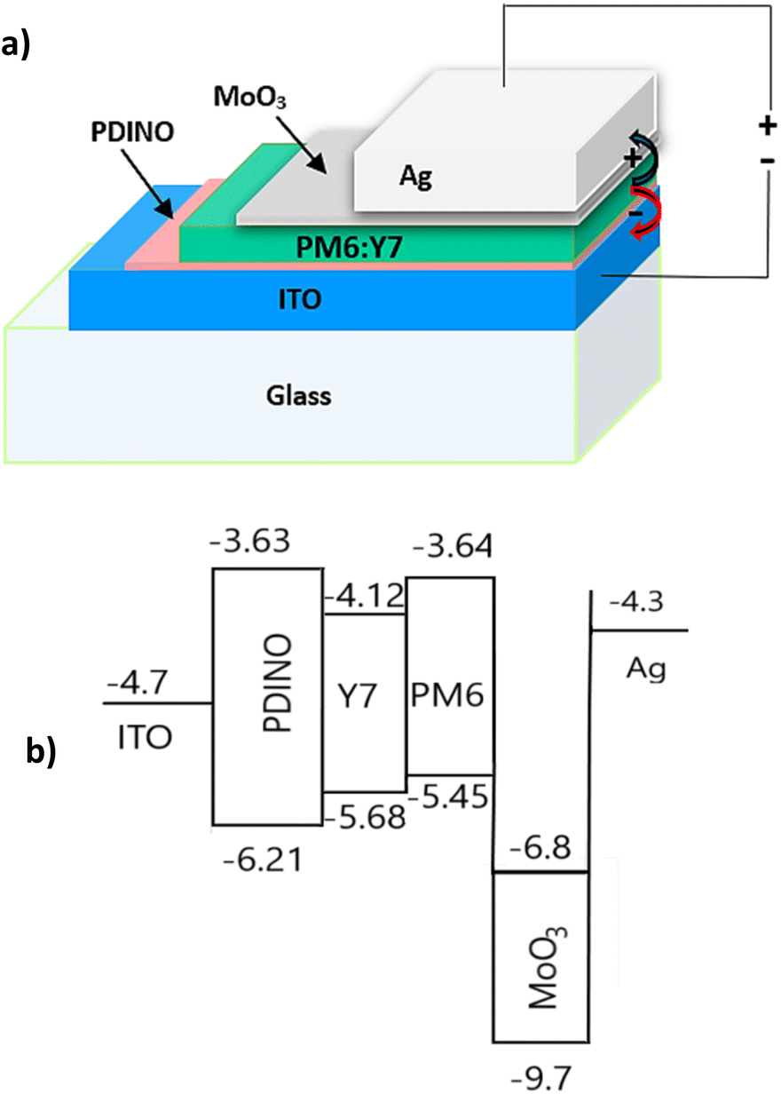 | ||
| Fig. 1 (a) Cell structure; (b) energy band diagram of the materials used in the iOSC under study. | ||
Table 1 shows a summary of the device performance parameters just after fabrication, such as open circuit voltage (VOC), short circuit current density (JSC), fill factor (FF), power conversion efficiency (PCE), and both series and shunt resistances (RS and RSH) of the iOSCs. The maximum PCE of the iOSCs was 9.14% and an average of 8.93 ± 0.16%. They also showed a JSC maximum of 22.5 mA cm−2 and an average of 21.14 ± 0.94 mA cm−2, a VOC maximum of 740 mV and an average of 726 ± 9.90, and a FF maximum of 60.51% and an average of 60 ± 0.95%. Similar results were obtained by Moustafa et al. in ref. 11 where the iOSCs were fabricated without additives using the same materials in the active layer (PM6:Y7). They also studied the effect of introducing 1-chloronaphthalene (CN), and the effect of thermal annealing on the morphology of the active layer.
| J SCavg [mA cm−2] | V OCavg [mV] | FFavg [%] | PCEavg [%] | PCEmax [%] | R Savg [Ω cm2] | R SHavg [Ω cm2] |
|---|---|---|---|---|---|---|
| 21.14 ± 0.94 | 726.00 ± 9.91 | 60.00 ± 0.95 | 8.93 ± 0.16 | 9.14 | 2.14 ± 0.16 | 202.50 ± 25.00 |
Degradation analysis of the iOSCs under darkness and continuous illumination
Fig. 2a shows the current density vs. voltage (J–V) characteristics of the best-performing iOSC after fabrication, under light (1.5G spectrum, 100 mW cm−2), for devices kept under dark and N2 environments. This figure also shows the experimental and modeled J–V curves at different times of degradation. Fig. 2b shows J–V curves under darkness for different times during 3552 h. The J–V curve named “fresh” was characterized immediately after the fabrication process at 0 h. Then, the devices were stored in the dark under a N2 environment at room temperature (RT) and a controlled relative humidity (RH) of 20–22%.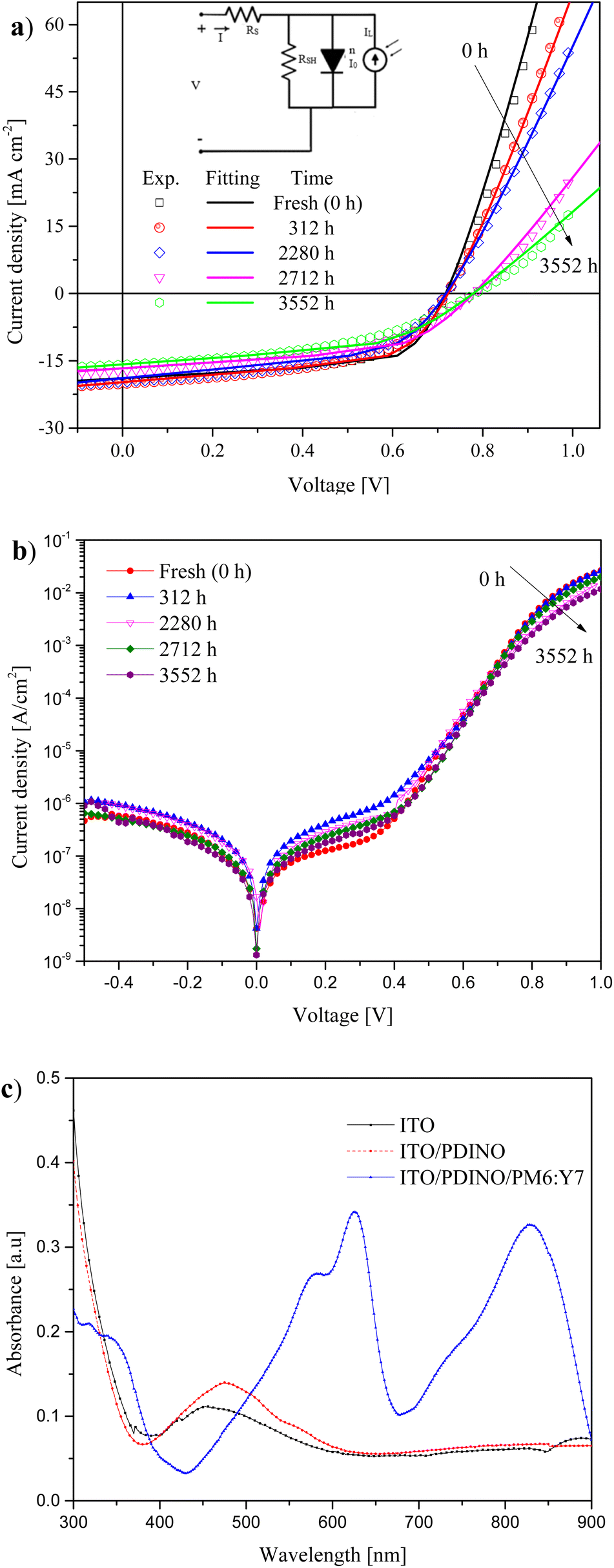 | ||
| Fig. 2 J–V characteristics of devices measured under (a) light (1 sun) and (b) darkness. (c) UV-vis optical characteristics of ITO, ITO/PDINO and ITO/PDINO/PM6:Y7. | ||
As can be observed in Fig. 2a, the J–V measurements were modeled using an equivalent circuit of one diode (inset in Fig. 2a).32 The extracted parameters from the fitting of the selected J–V curves are shown in Table 2. As reported in our previous studies,19,33,34 the ideality factor of the diode (n) represents the dominant transport mechanism in the device, where n = 1 (ideal diode) indicates that the diffusion mechanism is dominant in the device. However, a value of n = 2 indicates that recombination is the dominant mechanism, which is mainly caused by trap-assisted recombination.35,36 In our case, it is observed that n increased from 1.31 (fresh cell) to 1.46 after 3552 h. This suggests that the increasing trap density is minimal, and therefore the device degradation caused by trap-assisted recombination is small. On the other hand, saturation current density (J0) increased from 9.72 × 10⁻⁹ mA cm−2 to 1.87 × 10⁻⁸ mA cm−2 in the same period. The value of J0, related to the saturation current in OSCs, is associated with the number of charges capable of overcoming the energy barrier at the donor/acceptor interface in the active layer of the bulk heterojunction (BHJ) OSCs. J0 also represents the minority charge density near the interface of the BHJ. In this sense, if the device presents a greater J0, there is a greater recombination in the active layer.37–39 This slight increment in n and J0 is consistent with the great stability of VOC over time, observed in Fig. 3a. According to ref. 36–38, VOC is directly affected by n and inversely affected by J0.
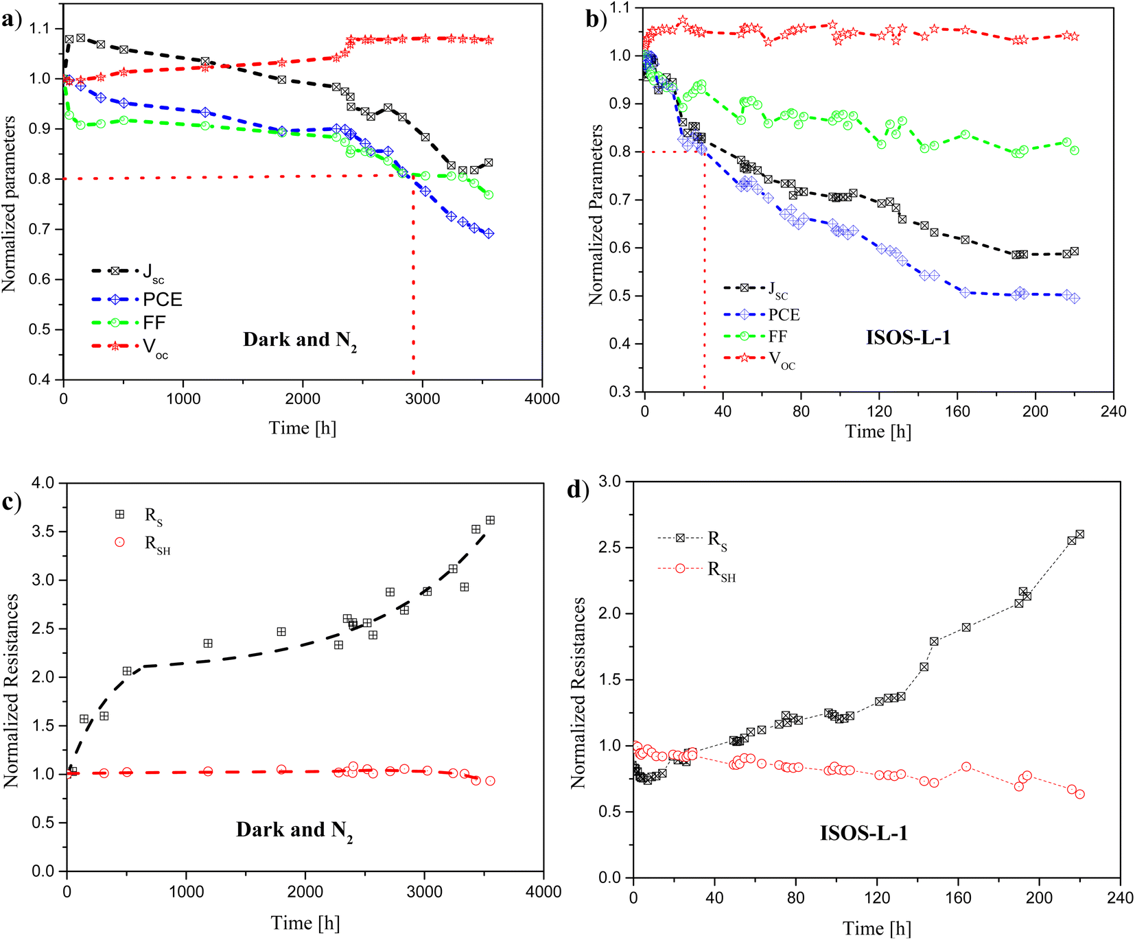 | ||
| Fig. 3 Normalized performance parameters over time: JSC, VOC, FF, and PCE of the iOSCs degraded under (a) dark and N2 environments, and (b) ISOS-L-1 protocols. Series resistance (RS) and shunt resistance (RSH) over time of the iOSCs degraded under (c) dark and N2 environments, and (d) ISOS-L-1 protocols. | ||
The absorbance measurements for the layers (ITO, ITO/PDINO and ITO/PDINO/PM6:Y7) are shown in Fig. 2c. In the UV-vis spectrum, it is observed that the absorbance of the ITO layer showed a peak centered at ∼460 nm.40 For the ITO/PDINO stack, the maximum of the spectrum red-shifted toward 480 nm, which is due to the absorption characteristics of the PDINO layer deposited on top of the ITO layer.41 After the deposition of the PM6:Y7 active layer, the absorption spectrum of the structure within the interval from 300 nm to 900 nm includes two new maximum peaks, located at 625 nm and 830 nm, respectively, which is consistent with the results reported in ref. 16.
The normalized performance parameters (VOC, JSC, FF, and PCE) are shown in Fig. 3a and b, for devices degraded under dark and N2 environments, and for devices photo-degraded following ISOS-L-1 protocols, respectively. As can be observed in Table 3, the times to reach 90%, 80%, and 50% of the initial PCE of the iOSCs (T90, T80, and T50, respectively) are 2363 h, 2918 h, and greater than 3552 h. This degradation analysis time is the longest reported for an inverted structure of OSCs using an ITO/PDINO/PM6:Y7 structure, degraded under similar environmental conditions. On the other hand, following the ISOS-L-1 protocols, the T90, T80, and T50 were 17 h, 31 h, and 220 h, respectively, where T80 is 3.6 times longer than that obtained in the recent reported work by Moustafa et al.12 using the same active layer and ETL, but V2O5 as the HTL. The photo-degradation analysis was done under the same illumination conditions. In our case, T80 was 11.6 times longer than that for iOSCs with the same active layer, but using ZnO as the ETL.12,42 This improvement in T80 is attributed to the use of MoO3 and PDINO18,43–45 instead of V2O5 and ZnO.
| Degradation conditions | T 90 [h] | T 80 [h] | T 50 [h] |
|---|---|---|---|
| Dark and N2 | 2363 | 2918 | >3552 |
| ISOS L-1 protocols | 17 | 31 | 220 |
It is important to remark that, during the first 300 min under continuous irradiation, the iOSCs demonstrated a highly photostable behavior, showing only a slight drop in PCE of 2%. In this sense, the devices exhibited an insignificant “burn in loss” degradation, which is commonly presented during the first operation minutes of the devices under light illumination. This phenomenon is associated with the intrinsic light-driven degradation due to the material properties, and the photochemical reaction of the ETL and HTL with the photoactive layer.19,46,47
The normalized PCE decays exponentially over time during the first 2400 h, and afterwards the decay ratio incremented. The JSC degradation presented an initial increase during the first hours of operation. Afterwards, it presented a similar behaviour to the PCE, suggesting that the behaviour of the PCE is given by the behaviour of the JSC. The slight increase in JSC can be attributed to the photochemical reactions in the active layer during the first measurements under illumination, resulting in an increment of the polymer conductivity, as reported in ref. 33 and 48. The JSC value reached 83% after 3552 h, see Fig. 3a.
The FF behaviour over time showed an exponential decay during the first hours of operation, and after 2280 h the decay ratio incremented. It is reported that RS can affect the FF, and therefore the behaviour of FF can be associated with the changes of RS over time observed in Fig. 3c.35
The VOC degradation behaviour was the most stable parameter. During the first 2500 h, it had a slight increase, keeping stable afterwards; similar behaviour is reported in ref. 19, 49 and 50. The VOC losses may arise from light-induced trap states/defects as described elsewhere.35,51 Therefore, the slight increase in VOC suggests that the trap density remains low, and therefore the device degradation caused by trap-assisted recombination is small. This agrees with the values of n and J0 shown in Table 2.
In general, compared to the other device performance parameters, VOC seems to be the least affected by the degradation in PM6:Y7-based iOSCs, while FF and JSC appear to suffer more by degradation, and consequently PCE. This suggests that the performance deterioration is probably associated with the charge extraction, which is correlated with the interlayer degradation of the device.
The values of the overall series resistance (RS) and the shunt resistance (RSH) were calculated from J–V measurements over time. Fig. 3c shows the normalized behaviour of RS over time. It is observed that RS increased exponentially as R0 + A0 × exp(R0 × t), until around 2100 h. Afterwards, it continues increasing at a faster rate in the form of R1 + A1 × exp((t − t0)/t1), where R0 and R1 are the relative initial resistances of the first and the second region, respectively. A0 and A1 are the degradation power factors of resistance, and t0 and t1 are the initial reference times of each region. Similar behaviour is reported in ref. 49 and 52. After 3552 h, the value of RS reached more than 3.5 times its initial value. RS mainly consists of the sum of the resistance due to the electrodes, the bulk active layer, and the interfacial contact resistance between the active layer and the electrodes,35 and it increases until 3336 h. After this, it started to decrease until 0.93 of the normalized initial value, decreasing from 202.5 Ω cm2 to 187.94 Ω cm2 after 3552 h.
On the other hand, the photo-degradation behaviour of the PCE, JSC and FF of iOSCs under continuous illumination presented an exponential decay over time (see Fig. 3b), showing that the behaviour of the PCE is given by the behaviour of the JSC. 49% of their initial PCE, and 59% of their initial JSC value were obtained after 220 h.
As can be observed in Fig. 3b, the VOC had a slight increase of 5% from the first operation hours under continuous light illumination of the iOSCs, after which it remained constant during 220 h. Since, according to ref. 12, 35 and 51, the VOC losses are due to the light-induced trap states/defects in the devices, we can conclude that our devices have lower photo-induced defects than those reported in ref. 12. One possibility for the reduction of states/defects in our devices can be attributed to using MoO3 instead of V2O5 as the HTL, which should avoid the photocatalytic reaction of the V2O5, contributing to the decomposition of the organic active layer.12,42
The morphology changes in the active layer, particularly the mixed region, cause degradation predominantly in the FF under illumination. Electron traps are formed due to rearrangement of polymers and diffusion-limited aggregation of NFAs to assemble small isolated acceptor domains under illumination. These electron traps cause losses mainly in FF and JSC.53 In our case, the devices reached 80% of FF after 220 h.
The reduction behaviour over time of JSC (Fig. 3b) can be attributed to the increment in RS, which can be related to a phase separation of the acceptor and donor domains, as well as to the photo-degradation of the organic layers, conducive to the formation of an isolation layer between the metallic contact and the active layer. The increase in RS reduces the collection of charge carriers, and the mobility. The value of RS after 220 h was nearly 3 times its initial value, as can be observed in Fig. 3d.19,48,54,55
Fig. 3d shows the normalized behaviour of RSH over time, which reached 63% of its initial value after 220 h. The reduction in RSH also affects the FF (see Fig. 3b).19
Impedance spectroscopy analysis
Impedance spectroscopy (IS) measurements were done to study the transport degradation processes taking place in the cell. A first analysis of IS was done on devices under dark and N2 environments. The measurements were carried out under dark conditions by applying a small AC excitation signal (50 mV) to the cell structure. The frequency in the IS measurements was swept from 1 kHz to 2 MHz. The data were collected at different time intervals to obtain the impedance spectrum at different times elapsed, to study the degradation issues related to the different interfaces present in the device. The first measurement was done right after fabrication. Samples were kept under dark and N2 conditions.The experimental data have been fitted by an equivalent electrical model using three resistor/capacitor (3 RC) circuits in series, as shown in Fig. 4a (inset). R1 is associated with the series resistance of the ITO layer; L with external measurement cables, C1 & R2 with the resistance and geometrical capacitance of PDINO, C2 & R3 with the active layer (PM6:Y7), and C3 & R4 with the MoO3 layer. In the ESI,† the fits of the IS measurements over time using the 2 RC and the 3 RC models are included, and the fitting parameters for both models are also presented (Tables S1 and S2†), showing a better adjustment with the 3 RC model, Fig. S4–S6.† The geometrical capacitance value of each layer was calculated according to Cg = εlayerε0A/Ln, where ε0 is the vacuum dielectric permittivity, A is the device area, εlayer is the relative dielectric permittivity of the corresponding layer, and Ln is the layer thickness. The calculated initial values for each layer are shown in Table 4.11,56–59
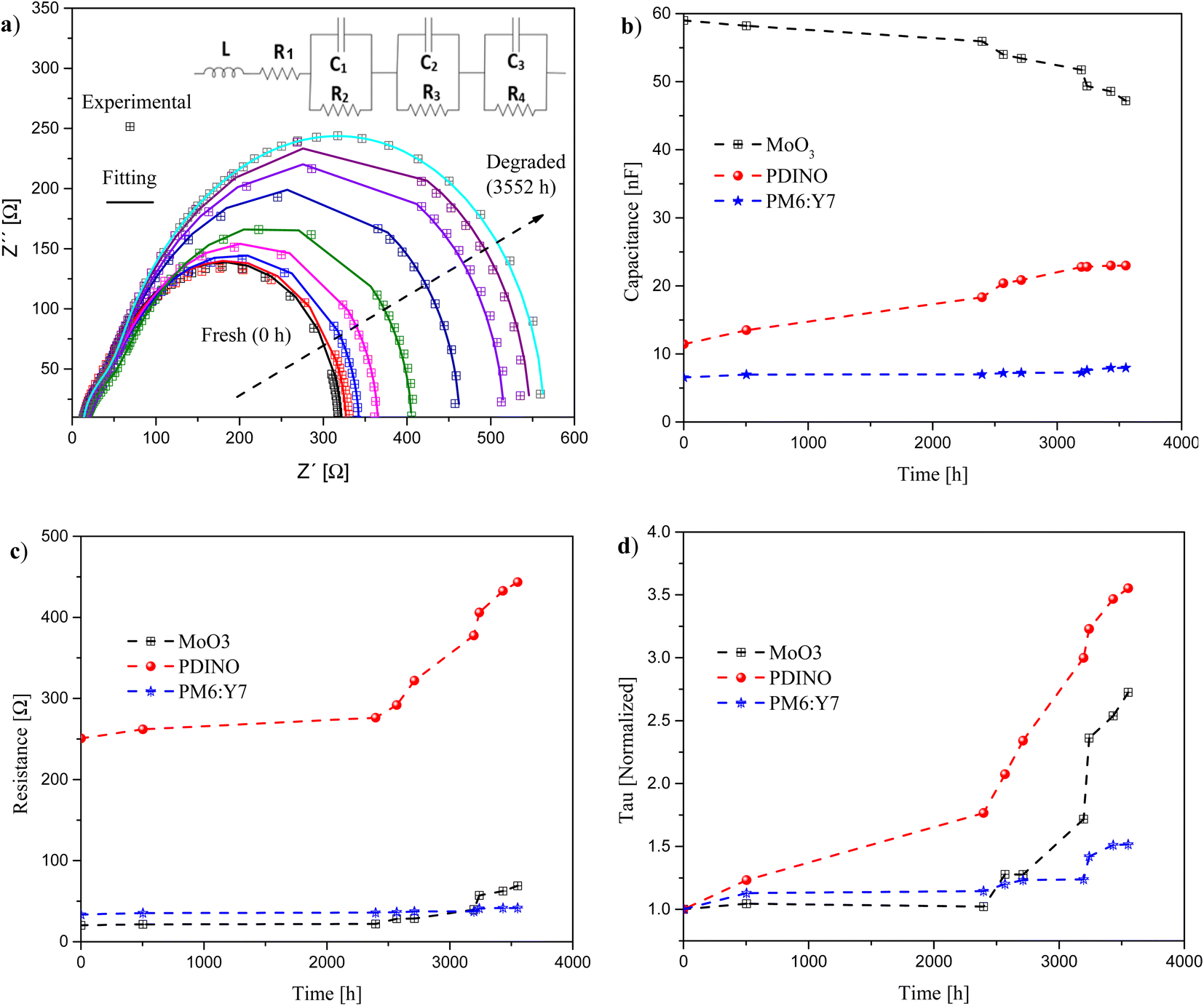 | ||
| Fig. 4 (a) Experimental (symbols) and fitting (lines) impedance spectra (IS) response over time for iOSCs measured under dark conditions at 0.78 V. (b) Capacitance, (c) resistance, and (d) Tau data extracted from the fitting of IS measurements. | ||
| Layer | L n (nm) | ε layer | Capacitance (nF) |
|---|---|---|---|
| PDINO | 41 | 5.00 | 9.72 |
| PM6:Y7 | 100 | 3.50 | 3.98 |
| MoO3 | 7.50 | 5.70 | 60.60 |
Fig. 4 shows the IS behaviour as the cell degrades. Fig. 4a shows Nyquist plots (experimental and fitting) for different degradation times, while Fig. 4b and c show the evolution of the extracted values over time of the capacitance and resistance associated with each layer, respectively. Finally, Fig. 4d shows the normalized behaviour of the time constant over time (Tau = R × C), using the extracted values for each layer.
As expected, the Nyquist plot diameter increases with degradation time (Fig. 4a), suggesting an increase in the overall resistance of the device.60
After 3552 h, the capacitance over time for the PDINO and active layer increased from 11.44 nF to 22.98 nF, and from 6.54 nF to 7.99 nF, respectively, see Fig. 4b. This increase of the capacitance over time suggests an increase of the charge accumulation in the layer, which can be associated with a worsening of charge carrier extraction, leading to the device degradation.61,62 This behaviour can possibly be attributed to deterioration of the interfaces which causes the accumulation of electrons at the PDINO/active layer, and/or at the ITO/PDINO interfaces.63 In this sense, the capacitance of the PDINO layer showed an increase of 100% of its initial value, while the active layer showed an increase of only 22%, suggesting that the degradation of the PDINO layer is the one determining the overall cell degradation. On the other hand, in the same figure, the capacitance of MoO3 shows a decrease from 59 nF to 47.2 nF, in the same period. This trend, together with the increase of the respective layer resistance, Fig. 4c, indicates that the film is losing gradually its conductivity, worsening the device behaviour.61 This behaviour of MoO3 capacitance over time agrees well with the results obtained in our previously reported work.19
It is important to notice that all resistances show an increase with time. But a lower increment is presented for the resistance of the active layer, showing an increment from 33.4 Ω to 41.6 Ω, while the PDINO and MoO3 resistance increased from 250.7 Ω to 443.4 Ω, and from 20.23 Ω to 68.91 Ω, respectively, as can be observed in Fig. 4c.
After calculating the Tau values over time for each layer, as expected, the greatest variation of Tau over time was observed for the PDINO layer, with an increment of 3.5 in the normalized value of Tau, followed by the MoO3 layer with an increment of 2.5. Finally, the Tau of the active layer showed the smallest ratio of increment of 1.5. From the above analysis, we can conclude that the layer that suffered the greatest degradation over time was the PDINO, followed by the MoO3 layer. It is important to mention that the PM6:Y7 mixture in the active layer showed a great stability, although contacting layers degraded significantly, and the active layer maintained its good initial characteristics throughout time.
It is important to mention that the strongest variation of all analysed layer parameters started approximately at the same elapsed time, around 2400 h, where performance parameters started to degrade more rapidly. The analysis after IS measurements confirmed that in the OSC using an ITO/PDINO/PM6:Y7 structure, the PDINO layer determines the overall cell degradation, while the active PM6:Y7 layer was the most stable over time.
A second analysis of IS measurements was done for devices under continuous irradiation (100 mW cm−2), following the ISOS-L-1 protocols to gain a better comprehension of the photo-degradation effects over each layer of the iOSC (Fig. 5). The measurements were done under similar conditions as for the devices under darkness. In this case, the devices were under illumination during each measurement. The experimental data were fitted using the same equivalent electrical model, consisting of three resistor/capacitor (3 RC) circuits in series, as shown in Fig. 4a (inset). This analysis also provides information regarding which layer plays the most important role in the behaviour of the device, in this case, under continuous illumination conditions.
 | ||
| Fig. 5 (a) Experimental (symbols) and fitting (lines) impedance spectra (IS) response over time for iOSCs measured under continuous irradiation (100 mW cm−2) at 0.78 V. (b) Capacitance, (c) resistance, and (d) Tau data extracted from the fitting of IS measurements. | ||
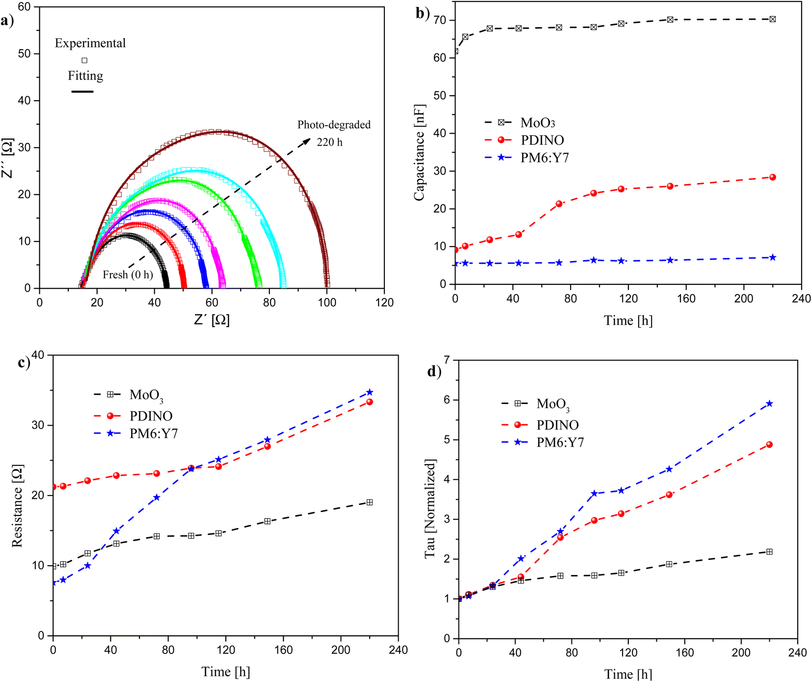
Fig. 5a shows typical Nyquist plots (experimental and fitting) that were obtained for the fresh and photo-degraded iOSCs over time. Again, all plots exhibited a semicircle shape, the arc diameter of which increases over time for the photo-degraded devices. This behaviour is related to the increase of the resistance of the devices due to the continuous light exposure.12
Fig. 5b and c show the evolution of the extracted values over time of the capacitance and resistance associated with each layer, respectively. To further determine which layer is more affected by the photo-degradation under illumination, we calculate the time constant (Tau = R × C) for each layer over time, as shown in Fig. 5d.
After 220 h under continuous illumination of the iOSCs, the capacitance values over time for the PDINO, active layer and MoO3 increased from 9.14 nF to 28.40 nF, from 5.50 nF to 7.11 nF, and from 61.81 nF to 70.30 nF, respectively, see Fig. 5b. The resistance values over time for the same materials increased from 21.22 Ω to 33.34 Ω, from 7.59 Ω to 34.70 Ω, and from 9.90 Ω to 19.00 Ω, respectively, see Fig. 5c.
A higher increment of the capacitance, 3 times its initial value, was observed for the PDINO layer. The capacitance of the active layer increased by 29%, while that of the MoO3 layer increased only by 14%. As can be observed in Fig. 5c, all resistances of the layers increased with time. The lowest increment of resistance is presented for the PDINO layer of 57%, followed by the MoO3 layer with an increment of 92%. The highest increment was presented by the active layer, showing 4.57 times its initial value.
From the Tau values over time, as expected, the greatest variation was observed for the active layer, with an increment of its normalized value up to 5.90 times. The normalized value of the Tau for the PDINO layer increased less, up to 4.88 times. The normalized value of Tau of the MoO3 layer showed the smallest ratio of increment of 2.18 times. These results indicate that the performance degradation of iOSCs under AM 1.5G illumination was mainly due to the photo-degradation of the organic layers, that is, the active and PDINO layers. Such degradation has been related to photochemical reactions inside and between organic layers, activated by the continuous exposure to light, when the device is in operation.64–66 In contrast the MoO3 inorganic layer showed the best stability under continuous illumination.
Experimental section
Materials
ITO-coated glass substrates with a nominal sheet resistance of 10 Ω per square and 220 nm of thickness were purchased from PsiOTec Ltd. PM6, Y7, and MoO3 were purchased from Sigma-Aldrich. PDINO was obtained from 1-material. Silver wire, with 99.99% purity, was obtained from Testbourne Ltd.Device fabrication
ITO coated glass substrates were cleaned in acetone, methanol, and isopropyl alcohol for 10 min in each one, after which they were exposed for 30 min under UV light.PDINO is diluted in methanol at a rate of 1.5 mg ml−1 and left shaking for 3 hours at 1000 rpm, after which it is spin coated at 3000 rpm for 30 s onto the ITO substrate.
The active blend of PM6:Y7 is prepared at a 1![[thin space (1/6-em)]](https://www.rsc.org/images/entities/char_2009.gif) :1 wt% dilution in CB, and left shaking at 1000 rpm, for 3 hours at 80 °C. Afterwards, the PM6:Y7 dilution is spin coated at 1500 rpm for 40 s onto the ITO substrate already covered by the PDINO layer.
:1 wt% dilution in CB, and left shaking at 1000 rpm, for 3 hours at 80 °C. Afterwards, the PM6:Y7 dilution is spin coated at 1500 rpm for 40 s onto the ITO substrate already covered by the PDINO layer.
The samples are annealed during 60 min at 90 °C, after which MoO3 is deposited by vacuum evaporation, followed by the deposition of Ag also by vacuum evaporation.
Device characterization
The current density–voltage (J–V) measurements of the unencapsulated iOSCs under light and darkness were performed at room temperature using a Keithley 2400 source-measure unit and a solar simulator (Abet Technologies model 11000 class Type A, Xenon arc). The light intensity of the AM 1.5G spectra was calibrated using an NREL certified monocrystalline silicon photodiode at 100 mW cm−2.
Film thicknesses of the deposited materials were measured using a Gaertner Scientific L2W16S633 ellipsometer.
The study was carried out on devices under dark and N2 environments and, following the ISOS-L-1 protocols.26
Impedance spectroscopy characterization was performed near VOC (0.78 V DC), superimposing an AC signal of 50 mV amplitude in the frequency range of 1 kHz to 2 MHz, to study the transport degradation processes taking place in the cell. The equivalent circuit consisted of three RC elements in series, each associated with one of the layers (ETL, active layer and HTL) present in the iOSC.
Conclusions
Inverted organic solar cells were fabricated using the PM6 (PBDB-T-2F):Y7 (BTP-4Cl) blend without any additive as the active layer, and PDINO and MoO3 as the ETL and HTL, respectively. The maximum obtained PCE for these devices was 9.14%, consistent with data previously reported by other research groups. A degradation analysis of these devices, for 3552 h, was performed for devices under dark and N2 environments, which as far as we know, is the longest performed for an inverted structure of OSCs using the above indicated materials. In addition, a photo-degradation aging test of the iOSCs under continuous exposure of AM 1.5G illumination conditions was performed following the ISOS-L-1 protocols.The performance parameters over time obtained from the illuminated J–V curves were analyzed. The T90, T80, and T50, observed for these devices under dark and N2 environments were 2363 h, 2918 h, and >3552 h, respectively, and following ISOS-L-1 protocols were 17 h, 31 h, and 220 h, respectively.
The analysis of the degradation of the device performance parameters under dark and N2 environments and, following the ISOS-L-1 protocols, showed that, in both studies, VOC seems to be the least affected. On the other hand, FF and JSC, and consequently the PCE, were more affected by degradation. The analysis also indicates that the main cause of degradation seems to be associated with problems with the charge extraction, caused by the degradation of a device layer, or at its contact with the nearby ones.
The IS measurements further indicated that the PDINO layer is the one determining the overall cell degradation, while the active layer showed the highest stability during the elapsed 3552 h for cells degraded under dark and N2 environments. The small increment observed in J0 and n is reflected in the slight variation and good stability observed in the VOC. This behaviour also suggests that the trap density remains low, and therefore the device degradation caused by trap-assisted recombination is small.
Under constant AM 1.5G illumination, following the ISOS-L-1 protocols, the IS results suggest that the performance degradation of the iOSCs is mainly due to the photo-degradation of the organic layers, that is the active and the PDINO layers, for which the normalized value in Tau increased up to 5.90, and 4.88 times, respectively. This work also confirms the higher stability observed for the iOSC, when a MoO3 layer is used as the HTL, which in this analysis showed the smallest ratio of increment in Tau of around 2.
Conflicts of interest
The authors declare no conflicts of interest.Acknowledgements
Ángel Sacramento and Magaly Ramírez acknowledge Consejo Nacional de Humanidades, Ciencias y Tecnologías (CONAHCYT) for supporting Postdoctoral Scholarships, under grants BPPA-20220711103224986-2580943 and BPPA-20220624083033039-2364083, respectively. Victor Balderrama specially acknowledges CONAHCyT for the support by “Investigadores por México CONAHCyT” through Project 2 and Project Number 299061, “Laboratorio Nacional SEDEAM CONAHCYT”. The authors also acknowledge Ing. D. Nápoles, Ing. G. Alvarez, Ing. I. Vitales, Ing. L. E. Santos and Ing. B. Ruan for their assistance in measurements and other laboratory activities during this work.References
- C. J. Brabec, M. Heeney, I. McCulloch and J. Nelson, Chem. Soc. Rev., 2011, 40, 1185–1199 RSC.
- Y. Cui, H. Yao, L. Hong, T. Zhang, Y. Tang, B. Lin, K. Xian, B. Gao, C. An, P. Bi, W. Ma and J. Hou, Natl. Sci., 2020, 7, 1239–1246 CAS.
- J. Lv, H. Tang, J. Huang, C. Yan, K. Liu, Q. Yang, D. Hu, R. Singh, J. Lee, S. Lu, G. Li and Z. Kan, Energy Environ. Sci., 2021, 14, 3044–3052 RSC.
- Y. Tong, Z. Xiao, X. Du, C. Zuo, Y. Li, M. Lv, Y. Yuan, C. Yi, F. Hao, Y. Hua, T. Lei, Q. Lin, K. Sun, D. Zhao, C. Duan, X. shao, W. Li, H. Yip, Z. Xiao, B. Zhang, Q. Bian, Y. Cheng, S. Liu, M. Cheng, Z. Jin, S. Yang and L. Ding, Sci. China: Chem., 2020, 63, 758–765 CrossRef CAS.
- M. B. Upama, N. K. Elumalai, M. A. Mahmud, M. Wright, D. Wang, C. Xu and A. Uddin, Sol. Energy Mater. Sol. Cells, 2018, 176, 109–118 CrossRef CAS.
- M. B. Upama, M. A. Mahmud, G. Conibeer and A. Uddin, Sol. RRL, 2020, 4, 1900342 CrossRef CAS.
- C. Yang, S. Zhang, J. Ren, M. Gao, P. Bi, L. Ye and J. Hou, Energy Environ. Sci., 2020, 13, 2864–2869 RSC.
- J. Yuan, Y. Zhang, L. Zhou, G. Zhang, H. L. Yip, T. K. Lau, X. Lu, C. Zhu, H. Peng, P. A. Johnson, M. Leclerc, Y. Cao, J. Ulanski, Y. Li and Y. Zou, Joule, 2019, 3, 1140–1151 CrossRef CAS.
- G. Zhang, X. K. Chen, J. Xiao, P. C. Y. Chow, M. Ren, G. Kupgan, X. Jiao, C. C. S. Chan, X. Du, R. Xia, Z. Chen, J. Yuan, Y. Zhang, S. Zhang, Y. Liu, Y. Zou, H. Yan, K. S. Wong, V. Coropceanu, N. Li, C. J. BRabec, J. L. Bredas, H. L. Yip and Y. Cao, Nat. Commun., 2020, 11, 3943 CrossRef CAS PubMed.
- S. Zhong, B. K. Yap, Z. Zhong and L. Ying, Crystals, 2022, 12, 168 CrossRef CAS.
- E. Moustafa, A. A. A. Torimtubun, J. Pallarés and L. F. Marsal, Sol. RRL, 2022, 6, 2100480 CrossRef CAS.
- E. Moustafa, M. Méndez, J. Pallarés and L. F. Marsal, Sol. Energy Mater. Sol. Cells, 2022, 248, 111985 CrossRef CAS.
- Y. Cui, H. Yao, J. Zhang, K. Xian, T. Zhang, L. Hong, Y. Wang, Y. Xu, K. Ma, C. An. C. He, Z. Wei, F. Gao and J. Hou, Adv. Mater., 2020, 32, 1908205 CrossRef CAS PubMed.
- A. Karki, J. Vollbrecht, A. J. Gillett, S. S. Xiao, Y. Yang, Z. Peng, N. Schopp, A. L. Dixon, S. Yoon, M. Schrock, H. Ade, G. N. M. Reddy, R. H. Friend and T. Q. Nguyen, Energy Environ. Sci., 2020, 13, 3679–3692 RSC.
- S. Bao, H. Yang, H. Fan, J. Zhang, Z. Wei and C. Cui, Adv. Mater., 2021, 33, 2105301 CrossRef CAS PubMed.
- E. Moustafa, M. Méndez, J. G. Sánchez, J. Pallarés, E. Palomares and L. F. Marsal, Adv. Energy Mater., 2023, 13, 2203241 CrossRef CAS.
- y. Chen, T. Liu, L. K. Ma, W. Xue, R. Ma, J. Zhang, C. Ma, H. K. Kim, H. Yu, F. Bai, K. S. Wong, W. Ma, H. Yan and Y. Zou, J. Mater. Chem. A, 2021, 9, 7481–7490 RSC.
- M. Ramírez-Como, E. Moustafa, A. A. A. Torimtubun, J. G. Sánchez, J. Pallarés and L. F. Marsal, in IEEE Latin American Electron Devices Conference (LAEDC), IEEE, Cancun, Mexico, 2022 Search PubMed.
- A. Sacramento, M. Ramírez-Como, V. S. Balderrama, J. G. Sánchez, J. Pallarés, L. F. Marsal and M. Estrada, J. Mater. Chem. C, 2021, 9, 6518–6527 RSC.
- M. Ramírez-Como, V. S. Balderrama, J. G. Sánchez, A. Sacramento, M. Estrada, J. Pallarés and L. F. Marsal, IEEE J. Electron Devices Soc., 2022, 10, 435–442 Search PubMed.
- Y. M. Sung, C. T. Chang, C. Tsao, H. Lin, H. Cha, P. Jiang, T. Liu, K. Chang, Y. Huang and J. Tsay, Nanoscale, 2023, 15, 3375–3386 RSC.
- H. Pan, L. Zuo, W. Fu, C. Fan, B. Andreasen, X. Jiang, K. Norman, F. C. Krebs and H. Chen, Org. Electron., 2013, 14, 797–803 CrossRef CAS.
- Y. Kanai, T. Matsushima and H. Murata, Thin Solid Films, 2009, 518, 537–540 CrossRef CAS.
- N. K. Elumalai, A. Saha, C. Vijila, R. Jose, Z. Jie and S. Ramakrishna, Phys. Chem. Chem. Phys., 2013, 15, 6831–6841 RSC.
- M. Y. Ameen, S. Pradhan, M. R. Suresh and V. S. Reddy, Opt. Mater., 2015, 39, 134–139 CrossRef.
- M. O. Reese, S. A. Gevorgyan, M. Jørgensen, E. Bundgaard, S. R. Kurtz, D. S. Ginley, A. Elschner, M. O. Reese, S. A. Gevorgyan, M. Jørgensen, E. Bundgaard, S. R. Kurtz, D. S. Ginley, D. C. Olson, M. T. Lloyd, P. Morvillo, E. A. Katz, A. Elschner, O. Haillant, T. R. Currier, V. Shrotriya, M. Hermenau, M. Riede, K. R. Kirov, G. Trimmel, T. Rath, O. Inganäs, F. Zhang, M. Andersson, K. Tvingstedt, M. Lira-Cantu, D. Laird, C. McGuiness, S. Gowrisanker, M. Pannone, M. Xiao, J. Hauch, R. Steim, D. M. DeLongchamp, R. Rösch, H. Hoppe, N. Espinosa, A. Urbina, G. Yaman-Uzunoglu, J.-B. Bonekamp, A. J. J. M. vanBreemen, C. Girotto, E. Voroshazi and F. C. Krebs, Sol. Energy Mater. Sol. Cells, 2011, 95, 1253–1267 CrossRef CAS.
- Y. Cui, H. Yao, J. Zhang, T. Zhang, Y. Wang, L. Hong, K. Xian, B. Xu, S. Zhang, J. Peng, Z. Wei, F. Gao and J. Hou, Nat. Commun., 2019, 10, 2515 CrossRef PubMed.
- J. Yao, B. Qui, Z. G. Zhang, L. Xue, R. Wang, C. Zhang, S. Chen, Q. Zhou, C. Sun, C. Yang, M. Xiao, L. Meng and Y. Li, Nat. Commun., 2020, 11, 2726 CrossRef CAS PubMed.
- K. Wang, C. Liu, T. Meng, C. Yi and X. Gong, Chem. Soc. Rev., 2016, 45, 2937–2975 RSC.
- J. Wu, J. Lee, Y. C. Chin, H. Yao, H. Cha, J. Luke, J. Hou, J. S. Kim and J. R. Durrant, Energy Environ. Sci., 2020, 13, 2422–2430 RSC.
- F. Tang, J. Wu, Z. Lin and X. Peng, ACS Appl. Mater. Interfaces, 2022, 14, 16487–16496 CrossRef CAS.
- F. J. García-Sánchez, B. Romero, D. C. Lugo-Muñoz, G. Del Pozo, B. Arredondo, J. J. Liou and A. Ortiz-Conde, Facta Univ., Ser.:Electron. Energetics, 2017, 30, 327–350 CrossRef.
- A. Sacramento, V. S. Balderrama, M. Ramírez-Como, L. F. Marsal and M. Estrada, Sol. Energy, 2020, 198, 419–426 CrossRef CAS.
- A. Sacramento, M. Ramirez-Como, V. S. Balderrama, S. I. Garduno, M. Estrada and L. F. Marsal, IEEE J. Electron Devices Soc., 2020, 8, 413–420 CAS.
- B. Qi and J. Wang, J. Mater. Chem., 2012, 22, 24315–24325 RSC.
- N. K. Elumalai and A. Uddin, Energy Environ. Sci., 2016, 9, 391–410 RSC.
- C. Waldauf, M. C. Scharber, P. Schilinsky, J. A. Hauch and C. J. Brabec, J. Appl. Phys., 2006, 99, 104503 CrossRef.
- C. Li, Z. Song, D. Zhao, C. Xiao, B. Subedi, N. Shrestha, M. M. Junda, C. Wang, C. S. Jiang, M. Al-Jassim, R. J. Ellingson, N. J. Podraza, K. Zhu and Y. Yan, Adv. Energy Mater., 2019, 9, 1803135 CrossRef.
- Z. He, C. Zhong, X. Huang, W. Y. Wong, H. Wu, L. Chen, S. Su and Y. Cao, Adv. Mater., 2011, 23, 4636–4643 CrossRef CAS PubMed.
- N. Biyikli, I. Kimukin, B. Butun, O. Aytur and E. Ozbay, IEEE J. Sel. Top. Quantum Electron., 2004, 10, 759–765 CrossRef CAS.
- Z. G. Zhang, B. Qi, Z. Jin, D. Chi, Z. Qi, Y. Li and J. Wang, Energy Environ. Sci., 2014, 7, 1966–1973 RSC.
- M. Cui, D. Li, X. Du, N. Li, Q. Rong, N. Li, L. Shui, G. Zhou, X. Wang, C. J. Brabec and L. Nian, Adv. Mater., 2020, 32, 2002973 CrossRef CAS.
- T. Kong, R. Wang, D. Zheng and J. Yu, Front. Chem., 2021, 9, 703561 CrossRef CAS.
- W. Wang, Z. Lin, X. Li, C. Zhang, T. Yang and Y. Liang, ACS Appl. Mater. Interfaces, 2022, 14, 18736–18743 CrossRef CAS.
- J. Yao, B. Qiu, Z. Zhang, L. Xue, R. Wang, C. Zhang, S. Chen, Q. Zhou, C. Sun, C. Yang, M. Xiao, L. Meng and Y. Li, Nat. Commun., 2020, 11, 2726 CrossRef CAS PubMed.
- L. Duan, X. Meng, Y. Zhang, H. Yi, K. Jin, F. Haque, C. Xu, Z. Xiao, L. Ding and A. Uddin, Mater. Chem. Front., 2019, 3, 1085–1096 RSC.
- A. Manor, E. A. Katz, T. Tromholt and F. C. Krebs, Adv. Energy Mater., 2011, 1, 836–843 CrossRef CAS.
- V. S. Balderrama, F. Avila-Herrera, J. G. Sánchez, J. Pallares, O. Vigil-Galán, L. F. Marsal and M. Estrada, IEEE J. Photovolt., 2016, 6, 491–497 Search PubMed.
- A. A. A. Torimtubun, M. Méndez, J. G. Sánchez, J. P. E. Palomares and L. F. Marsal, Sustainable Energy Fuels, 2021, 5, 6498–6508 RSC.
- V. S. Balderrama, M. Estrada, P. L. Han, P. Granero, J. Pallarés, J. F. Borrull and L. F. Marsal, Sol. Energy Mater. Sol. Cells, 2014, 125, 155–163 CrossRef CAS.
- N. Gasparini, S. H. K. Paleti, J. Bertrandie, G. Cai, G. Zhang, A. Wadsworth, X. Lu, H. L. Yip, I. McCulloch and D. Baran, ACS Energy Lett., 2020, 5, 1371–1379 CrossRef CAS.
- V. Singh, Curr. Appl. Phys., 2017, 17(11), 1450–1454 CrossRef.
- M. B. Upama, M. Wright, M. A. Mahmud, N. K. Alumalai, A. M. Soufiani, D. Wang, C. Xu and A. Uddin, Nanoscale, 2017, 9, 18788–18797 RSC.
- N. Grossiord, J. M. Kroon, R. Andriessen and P. W. M. Blom, Org. Electron., 2012, 13, 432–456 CrossRef CAS.
- X. Wang, C. X. Zhao, G. Xu, Z. K. Chen and F. Zhu, Sol. Energy Mater. Sol. Cells, 2012, 104, 1–6 CrossRef CAS.
- T. A. A. A. Torimtubun, J. G. Sánchez, J. Pallarés and L. F. Marsal, Sustainable Energy Fuels, 2020, 4, 3378–3387 RSC.
- R. C. I. MacKenzie, V. S. Balderrama, S. Schmeisser, R. Stoof, S. Greedy, J. Pallare`s, L. F. Marsal, A. Chanaewa and E. von Hauff, Adv. Energy Mater., 2016, 6, 1501742 CrossRef.
- S. Torabi, F. Jahani, I. V. Severen, C. Kanimoszhi, S. Patil, R. W. A. Havenith, R. C. Chiechi, L. Lutsen, D. J. M. Vanderzande, T. J. Cleij, J. C. Hummelen and L. J. A. Koster, Adv. Funct. Mater., 2015, 25, 150–157 CrossRef CAS.
- G. Garcia-Belmonte, A. Munar, E. M. Barea, J. Bisquert, I. Ugarte and R. Pacios, Org. Electron., 2008, 9, 847–851 CrossRef CAS.
- E. Von Hauff, J. Phys. Chem. C, 2019, 123, 11329–11346 CrossRef CAS.
- G. del Pozo, B. Arredondo, B. Romero, G. Susanna and F. Brunetti, Sol. Energy, 2017, 144, 105–110 CrossRef CAS.
- S. K. Gupta, L. S. Pali and A. Garg, Sol. Energy, 2019, 178, 133–141 CrossRef CAS.
- B. Arredondo, B. Romero, M. J. Beliatis, G. Del Pozo, D. Martín-Martín, J. C. Blakesley, G. Dibb, F. C. Krebs, S. A. Gevorgyan and F. A. Castro, Sol. Energy Mater. Sol. Cells, 2018, 176, 397–404 CrossRef CAS.
- J. Razzell-Hollis, J. Wade, W. C. Tsoi, Y. Soon, J. Durrant and J. S. Kim, J. Mater. Chem. A, 2014, 2, 20189–20195 RSC.
- T. Liu, Q. C. Burlingame, M. R. Ivancevic, X. Liu, J. Hu, B. P. Rand and Y. L. Loo, Adv. Energy Mater., 2023, 13, 2300046 CrossRef CAS.
- H. Bin, J. Wang, J. Li, M. M. Wienk and R. A. J. Janssen, Adv. Mater., 2021, 33, 2008429 CrossRef CAS PubMed.
Footnote |
| † Electronic supplementary information (ESI) available. See DOI: https://doi.org/10.1039/d3se00977g |
| This journal is © The Royal Society of Chemistry 2024 |