
Powerful drying and doping strategies for enhancing the thermoelectric performance of tellurium nanostructures prepared via green hydrothermal synthesis†
In Ho
Kim
and
Yong Jin
Jeong
 *
*
Department of Materials Science and Engineering, Korea National University of Transportation, Chungju 27469, Republic of Korea. E-mail: yjjeong@ut.ac.kr; Tel: +82-43-841-5383
First published on 21st November 2023
Abstract
Tellurium (Te), a well-known p-type semiconductor with a narrow bandgap, is used as a thermoelectric material in various polycrystalline forms such as Bi–Te, Pb–Te, and Sn–Te compounds. In particular, Te nanostructures have gained significant interest in various fields such as piezoelectrics, gas sensors, and energy conversion application; therefore, efforts have been made recently to enhance the thermoelectric performance of the Te family by using nanostructures engineered through various methods. This requires controlling the nanoscale properties of materials and suggesting effective doping strategies to enhance their electrical conductivity and Seebeck properties. Herein, we report an effective drying and solution-based doping approach to enhance the thermoelectric properties of Te nanostructures prepared via green hydrothermal synthesis. The freeze-drying process can form a three-dimensional porous structure of the Te nanostructured film, leading to an effective diffusion of the dopant solution and thereby improving the doping efficiency. Consequently, the effective doping of In under optimized conditions improves the electrical conductivity and power factor of Te nanostructures, demonstrating that the combination of freeze-drying and sequential solution-based doping is a promising approach for improving thermoelectric performance. This study contributes significantly to the development of solution-based doping of Te-based nanostructures for functional thermoelectric power applications.
1. Introduction
As the demand for electricity increases, the consumption of fossil fuel-based energy sources has led to excessive waste heat generation, thereby triggering climate change issues. In response, alternative energy systems, such as new energy sources including wind, hydropower, solar, nuclear, and fuel cells, are being developed and introduced to solve the waste heat problem. Thermoelectricity, with its unique ability to convert heat into electricity, has been extensively studied for its potential in energy harvesting and is emerging as a promising approach to sustainable energy solutions for automotive, aerospace, and electronic chips.1,2 Atomistic material design and process development are essential to increase the efficiency of thermoelectric power generation; hence, significant efforts have been made to improve the performance of typical thermoelectric materials such as tellurium (Te).3,4 Te-based chalcogen compounds have been predominantly used as excellent thermoelectric materials in compounds such as Bi2Te3,5 PbTe,6 Sb2Te3,7 and Ag2Te.8 Furthermore, Te nanostructures are also p-type semiconductors with a narrow band gap of 0.35 eV (ref. 9) that can be actively applied to energy and electronic devices.10–12 The natural abundance of pure Te in the earth's crust is low (around 0.02 ppm), similar to that of platinum (Pt),13 so utilizing Te requires a process to reduce Te compounds that exist in the ionically bound state, often utilizing techniques such as solution-based reducing synthesis.14 Employing nanostructures is a strategy for advancing thermoelectric material development, aiming to increase the Seebeck coefficient (α) and to decrease the lattice thermal conductivity.15,16 Te has a hexagonal crystal structure and grows helically along the c-axis,17–19 which is conducive to the formation of one-dimensional (1D) nanostructures such as wires, needles, and rods without the need for surfactants or pH adjustment.20 In other words, Te is a relatively easy material to induce crystal growth, allowing nanostructures to be developed under mild conditions without toxic chemicals such as hydrazine; this is ideal for implementing green energy conversion materials.Solution-phase doping is an effective method to further increase the thermoelectric properties of Te nanostructures from green chemistry.21 The doping methods include (1) adding dopants during the reduction of Te precursors to obtain doped Te nanostructures (i.e., solution mixing) and (2) doping through diffusion of dopants by dropping dopant solutions after the formation of Te nanostructures (i.e., sequential process).22 In solution mixing, dopants can affect the crystal growth of Te nanostructures, determining the thermoelectric properties through a combination of their doping effect and structural changes. Meanwhile, in the sequential process, doping can be performed after obtaining good-quality Te nanostructures that are effective for thermoelectric applications. Thus, the thermoelectric properties can be further improved by the effective doping of dopants while maintaining the already formed good-quality Te nanostructures. For this sequential doping process, one major consideration is that the dopant should sufficiently diffuse into the nanostructured film to ensure a uniform and effective doping. Along with the development of Te-based thermoelectric materials, the process strategy for the Te nanostructure fabrication, the selection of optimal dopant candidates, and the doping conditions for Te nanostructures need to be carefully considered to enhance the doping efficiency and thermoelectric performance.
In this paper, we propose a freeze-drying and sequential doping process to achieve an optimized thermoelectric material for Te nanostructures prepared through a green reduction method. Instead of using hydrazine hydrate to reduce the Te precursor during hydrothermal synthesis, eco- and bio-friendly glucose was used as a stabilizer and reducing agent to determine its suitability for the green synthesis of Te nanostructures. Solution-phase doping through a sequential process was adopted to improve the performance of dried Te nanostructure samples, and the doping properties of Te nanostructures prepared using two drying methods, freeze-drying and vacuum drying, were compared. In the sequential doping process using indium (In) dopants, the Te samples prepared by freeze-drying could establish a 3D porous structure of Te nanostructured films with sufficient interfaces to promote effective dopant diffusion, thereby improving the doping efficiency and thermoelectric performance.23 Furthermore, the In doping efficiency as a function of Te nanostructure processing conditions was studied, suggesting a strategy to optimize the doping process of Te nanostructures prepared by green chemistry.
2. Experimental section
Preparation of Te nanostructures from hydrothermal synthesis and drying methods
Approximately 140 mg sodium tellurite (Aldrich Co.) and 4 g D-(+)-glucose (Alfa Aesar Co.) were mixed in 80 ml deionized water (DIW). This mixture was placed in a 100 ml Teflon-lined stainless-steel autoclave and stirred at room temperature until complete dissolution of the substances was achieved. After completely sealing the autoclave, Te nanostructures were obtained by heating in ovens at the given temperature for 12 h. After the heating process was completed, the autoclave was allowed to cool gradually in ambient air. Once the solution had fully cooled, it was placed in 50 ml conical tubes with 40 ml in each tube and then vacuum filtered for the fabrication of films with consistent thickness. For vacuum filtration, the polyvinylidene fluoride (PVDF) membrane filter with a diameter of 47 mm and a pore size of 0.2 μm was cleansed using pure ethanol (EtOH) and acetone. Subsequently, the well-dispersed Te nanostructure solution (40 ml) was fabricated into films by pouring it onto the membrane filter installed in the vacuum filtration apparatus. Then, the films were washed using DIW and EtOH, followed by drying via (1) vacuum drying and (2) freeze drying approaches, as illustrated in Fig. 1a. For vacuum drying, the Te nanostructured films were stored in a vacuum oven at 60 °C for 12 h without any additional pretreatment immediately after filtration. In contrast, freeze drying involved a pre-treatment process in which the films were initially subjected to 24 h of freezing at −50 °C in a freezer. After pre-treatment, a 12 h freeze drying process was performed under conditions of −80 °C and 5 mTorr pressure, as previously set in the freeze dryer. | ||
| Fig. 1 Experimental schematics showing (a) the drying procedure of the as-synthesized Te and (b) In doping procedure of the prepared Te nanostructure film. (c) Reduction mechanism of sodium tellurite with the glucose. | ||
Solution-phase doping of In to Te nanostructured films
First, 0.036 M indium(III) chloride (Aldrich Co.) in ethylene glycol (Aldrich Co.) (10 ml) was placed in a vial, and the solution was stirred with a magnetic bar at room temperature. After stirring for 1 h to completely dissolve the In precursor, a transparent solution was obtained. Following the procedure outlined in Fig. 1b, a 1 ml syringe with a 0.2 μm polytetrafluoroethylene (PTFE) syringe filter was used to uniformly drop the precursor solution across the dried Te nanostructured films. For a sufficient reaction between the precursor and Te nanostructures, the samples were stored at room temperature for 1 h. The fabricated In-doped Te films were washed with EtOH and dried at 60 °C for 12 h in a vacuum oven.Characterization of Te samples
To compare the thermoelectric properties of the Te samples fabricated using several production processes, a probe station with a home-built measurement system (Keithley 2636B/2182A/2700) was used to determine S of the samples. The sample preparation process for the thermoelectric measurements is shown in Fig. S1.† The electrical conductivity (σ) was determined from the sheet resistance (using a four-probe method) and thickness of the sample. Finally, the power factor (PF) was calculated using α and σ. To analyze the material characteristics, the morphology, elemental composition, and crystal structure of the prepared Te samples were investigated using scanning electron microscopy (SEM, Thermo Scientific Co. Prisma E), energy-dispersive X-ray spectroscopy (EDS), and high-resolution X-ray diffraction (XRD, Bruker Co. D8 Advance). A surface composition analysis was performed using X-ray photoelectron spectroscopy (XPS; Thermo Scientific Co. K-Alpha+). For XPS analysis, a survey scan was conducted, followed by narrow scans of O, Te, and In. EDS and XPS analyses were used to determine the presence and mechanism of doping in the doped samples, with a particular focus on In doping.3. Results and discussion
Owing to its significant toxicity to humans and the environment, hydrazine, which was traditionally used as a reducing agent, is not environmentally suitable for producing thermoelectric materials used in alternative energy sources.24,25 Instead, the glucose system has been confirmed to readily form nanostructures during the synthesis process without requiring additional surfactants.20 Fig. S2† presents the results of SEM analysis performed after synthesizing using glucose and hydrazine hydrate under the same synthesis conditions. As observed in the SEM images, nanostructure synthesis occurred sufficiently with glucose alone, without requiring other chemicals. Glucose serves as a reducing agent, effectively reducing sodium tellurite to generate Te nuclei, while concurrently acting as a surfactant and reducing the free energy of Te, following the mechanism shown in Fig. 1c. Te nuclei adsorbed on the surfactant in the solution play the role of crystal seeds, simultaneously adsorbing the surrounding Te atoms and gradually undergoing natural c-axis growth owing to the anisotropic growth characteristics of Te.20 The research involved not only optimizing the green synthesis conditions of Te nanostructures but also enhancing the thermoelectric performance through an optimal drying process and solution-phase doping. The sequential doping efficiency and thermoelectric performance of Te nanostructured films can be improved by constructing vertical 3D structures with sufficient interfaces and boundaries to facilitate effective dopant diffusion. A freeze-drying process approach was used to build 3D porous structures of Te nanostructured films.23Fig. 2a and b show the SEM images of Te nanostructured films prepared by hydrothermal synthesis and vacuum filtration according to the drying conditions. Despite synthesis temperatures being near 100 °C, hydrothermal synthesis was utilized to prevent solvent evaporation and minimize heat loss. The Te nanostructure film synthesized at 100 °C was dried by vacuum drying and freeze-drying, and no change was observed in the 1D wire-like morphology with the change in the drying conditions. The Te nanostructure samples synthesized at 80 °C and 120 °C also showed no change in the nanostructure morphology with drying conditions. High-resolution XRD (λ = 1.54 Å) analysis of the Te nanostructure samples was further performed to confirm the crystal growth phase according to the drying conditions. No difference was observed in the Te nanostructure crystal phase between vacuum drying and freeze-drying; pattern signals corresponding to a typical hexagonal lattice structure of Te were observed that conformed to JCPDS 36-1452 (Fig. 2c). | ||
| Fig. 2 SEM images of Te nanostructures from (a) vacuum-drying and (b) freeze-drying methods. (c) XRD pattern spectra of the Te nanostructures from two drying methods. Plots showing (d) α and σ and (e) power factor of Te nanostructure films depending on the drying and doping conditions. (f) Schematic illustration showing the mechanism of formation of Te nanostructure films in the two drying methods. | ||
Although negligible differences existed in the morphology and crystalline phase of the Te nanostructures depending on the drying conditions, the thermoelectric performance analysis showed differences in the performance depending on the drying conditions, as presented in Table 1 and Fig. 2d and e. Prior to doping, the freeze-dried samples exhibited relatively low σ values compared to the vacuum-dried samples, resulting in a power factor approximately 25% less than that of the vacuum-dried samples. The low σ of the freeze-dried samples might be because of the empty space between the nanowires, as shown in Fig. 2f. During freeze-drying, the H2O present as ice sublimated, leaving voids, resulting in lower density between the nanowires.23 However, in the case of vacuum-drying, moisture in the liquid state acted in the opposite direction during drying,26 causing the structures to become denser and resulting in a smoother connection between the nanowires as compared with the freeze-dried samples. This resulted in better vacuum-dried samples with a more compact structure. However, after the In-doping process, the thermoelectric performances of both samples were reversed. The In doping of the freeze-dried samples showed a considerably greater improvement in σ performance, resulting in an average power factor (PF), calculated using PF = σα2, of 51.81 μW mK−2 that was 58% higher than that of the vacuum-dried and In-doped samples. This significant increase in the performance of the freeze-dried Te samples could probably be attributed to the ease of solution penetration into the voids between the structures after freeze-drying and to more efficient doping than in the case of vacuum drying. In short, the freeze-dried samples showed a greater improvement in performance than the vacuum-dried samples when comparing the performance before and after doping, suggesting that the freeze-drying conditions were more optimized for sequential doping via the solution route.
| Drying condition | Avg. σ (S cm−1) | Avg. α (μV K−1) | Avg. PF (μW mK−2) |
|---|---|---|---|
| Vacuum | 2.53 | 322.69 | 24.83 |
| Vacuum drying and doping | 2.87 | 337.36 | 32.69 |
| Freeze | 1.52 | 349.52 | 18.54 |
| Freeze drying and doping | 5.84 | 297.84 | 51.81 |
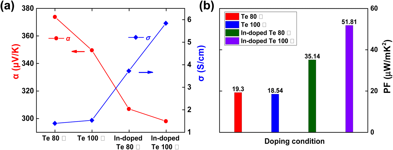
Having determined a suitable freeze-drying condition for the solution-phase doping process, we investigated the difference in post-sequential doping performance depending on the Te nanostructures prepared at different synthesis temperatures. Fig. 3 shows the SEM/EDS measurement images before and after In doping of Te for each synthesis temperature (80 °C/100 °C). Irrespective of the synthesis temperature, no significant change was observed in the nanostructure morphology before and after sequential doping (Fig. 3a–d), and the EDS mapping analysis revealed that In was present in the Te nanostructure after sequential doping (Fig. 3e–h and S3†). The thermoelectric performance of Te before and after In doping was analyzed for each synthesis temperature (80 °C/100 °C). In the case of 120 °C (Fig. S4†), although no differences existed in the XRD and SEM analysis results, a lower thermoelectric performance was measured as compared with 80 °C/100 °C. Therefore, this temperature was determined to be unsuitable as an optimal synthesis temperature. As noted from Fig. 4a and Table 2, the σ values of the samples synthesized at 80 °C and 100 °C were 1.38 S cm−1 and 1.52 S cm−1, respectively. However, α for the sample synthesized at 80 °C was 373.78 μV K−1 that was higher than that of the sample synthesized at 100 °C. After sequential doping with In, both samples showed an increase in σ owing to the increase in carrier concentration, with a corresponding decrease in α.27 The PF also exhibited an increase of approximately 2–3 times for both samples after In doping (Fig. 4b). Notably, the thermoelectric performance of the sample synthesized at 100 °C increased considerably more after doping than that of the sample synthesized at 80 °C. The PF of the sample synthesized at 100 °C increased approximately 2.8 times from 18.54 μV mK−2 to 51.81 μV mK−2 and that of the sample synthesized at 80 °C increased approximately 1.8 times from 19.30 μV mK−2 to 35.14 μV mK−2. The Hall effect measurement (Table S1†) also supported that the charge carrier concentration and the mobility of the Te sample synthesized at 100 °C were improved by solution-state doping with In. These results confirmed that the Te nanostructure synthesized at 100 °C was optimized for sequential doping. We also measured the thermoelectric performance of the samples after doubling (1) the dopant concentration and (2) the doping process time, respectively. Fig. S5† includes thermoelectric performances of pristine Te (without performing In doping), In-doped Te sample with 0.036 M dopant concentration, In-doped Te sample with 0.072 M dopant concentration (2 times higher doping concentration), and In-doped Te sample with 0.036 M for 2 h (2 times longer doping process). The σ increased with increasing indium doping concentration, while the α decreased slightly. The calculated PF increased when the doping concentration was doubled; however, the viscosity of the dopant solution appeared to increase when the concentration was doubled, which could be a limitation for a uniform doping process (not shown). Meanwhile, it could be found that the thermoelectric performance with increasing reaction time did not show a significant trend in the direction of improvement, indicating that the doping process for 1 hour was sufficient to fully dope the freeze-dried Te sample.
 | ||
| Fig. 3 SEM images of Te nanostructures at (a) 80 °C and (b) 100 °C. SEM images of the In-doped Te nanostructure at (c) 80 °C and (d) 100 °C. EDS mapping images of (e) Te and (f) In in the In-doped Te nanostructure at 80 °C. EDS mapping images of (g) Te and (h) In in the In-doped Te nanostructure at 100 °C. | ||
 | ||
| Fig. 4 (a) α and σ and (b) power factor of Te nanostructure films depending on the synthesis temperature and doping conditions. | ||
| Temperature (°C) | Avg. σ (S cm−1) | Avg. α (μV K−1) | Avg. PF (μW mK−2) |
|---|---|---|---|
| Te 80 °C | 1.38 | 373.78 | 19.30 |
| Te 100 °C | 1.52 | 349.52 | 18.54 |
| In-doped Te 80 °C | 3.72 | 306.78 | 35.14 |
| In-doped Te 100 °C | 5.84 | 297.84 | 51.81 |
Furthermore, we prepared an as-assembled prototype TEG with the optimized Te nanostructure samples and measured the output voltage generation depending on the temperature differences (ΔT), as shown in Fig. S6.† The output voltage was monotonically increased with increasing ΔT, showing 4.85 mV at ΔT = 4 K for the 4-leg sample. The slope of the fitted line between the output voltage and ΔT was calculated to be 1212.6 μV K−1 for the 4-leg sample, similar to 4 times the average α value of the In-doped Te 100 °C.
To identify the reasons for Te nanostructures synthesized at 100 °C acquiring superior thermoelectric performance with the doping process to those synthesized at 80 °C, the crystal structure of each sample was investigated using XRD (Fig. 5a). The XRD patterns of the as-synthesized sample included Te crystalline peaks (JCPDS 36-1452);28 however, the Te nanostructures synthesized at 80 °C also included TeO2 crystalline peaks (JCPDS 78-1713).29 This result implied that the Te nanostructure sample synthesized at 80 °C comprised two phases where certain TeO2 crystals existed independently of the Te crystals. Presumably, at low temperature synthesis conditions, such as 80 °C, the glucose-based green chemistry did not fully reduce the Te precursor; therefore, certain Te4+ ions existed as oxides. The XRD patterns of the In-doped samples did not differ from those of the undoped samples, indicating that the addition of In was atomically doped without creating another crystalline phase. The information on the chemical bonding was obtained using XPS. As shown in Fig. 5b, all the hydrothermally synthesized samples showed Te-related signals (Te 4d, Te 4s, Te 3d, Te 3p, and Te 3s). C 1s signals also appeared owing to the presence of residual glucose or small carbonaceous molecules adsorbed on the surface of the Te nanostructures.30,31Fig. 5c shows the XPS results for the Te 3d signals of the samples. In the Te 3d spectra, oxide (TeO2) signals were observed under both synthesis conditions. Inferring from the results that the pattern corresponding to TeO2 was not present in the XRD for the sample synthesized at 100 °C, the small signal of TeO2 detected indicated that the oxide was only formed on the surface of the Te nanostructures. In the XPS spectra, as shown in Fig. 5d, an In signal was detected for each doped sample.
 | ||
| Fig. 5 (a) XRD pattern spectra of Te nanostructures depending on the synthesis temperature and doping conditions. Comparative XPS spectra showing (b) the wide scope, (c) the Te 3d peak, and (d) In 3d peak of the nanostructures depending on the synthesis temperature and doping conditions. (e) Schematic showing the mechanism of In doping. | ||
Based on the XRD and XPS results, the In doping mechanism of the Te nanostructured samples was deduced, as shown in Fig. 5e. When solution-phase sequential doping was performed, the TeO2 phase formed around the surface of Te nanowires encountered ethylene glycol and released Te4+ ions from the oxide, and In3+ ions present in the dopant solution took their place, thereby generating holes owing to charge compensation and increasing σ. However, the samples synthesized at 80 °C appeared to be relatively unresponsive to doping because a separate TeO2 phase was grown (as confirmed by XRD patterns) rather than the Te surface-limited oxide. Low-temperature hydrothermal synthesis conditions did not allow sufficient reduction during synthesis, producing a separate secondary-phase product from the TeO3− state precursor to TeO2,20 where TeO2 remained chemically stable. This independent and stable TeO2 was not prone to In substitution, and even if it were, it would not contribute to the increased conductivity.
4. Conclusion
In summary, the optimal drying and doping strategies for Te nanostructures prepared using green synthesis methods were studied to enhance their thermoelectric performance. Solution-phase doping of Te nanostructured films prepared under different drying conditions was performed. The freeze-drying approach was observed to be more effective for In doping because the formation of 3D porous structures in the freeze-dried Te sample facilitated the penetration of the dopant solution and enabled efficient In doping. To determine the optimal synthesis temperature for solution-phase doping, the samples synthesized at temperatures of 80 °C and 100 °C were observed to have no obvious effect on the nanostructure morphology; however, the samples synthesized at 100 °C showed better In doping effect and thermoelectric performance. The XRD and XPS results revealed that the TeO2 present on the surface of Te nanostructures synthesized at 100 °C was doped with In3+ resulting in an effective doping, whereas the sample synthesized at 80 °C had a lower doping efficiency owing to the presence of an independent TeO2 phase. Collectively, this study confirms the feasibility of effective thermoelectric performance enhancement through solution-phase In doping of Te nanostructures, that can be combined with a freeze-drying process to further enhance the potential of solution-phase doping in the fabricated films.Author contributions
In Ho Kim: formal analysis, investigation, data curation. Yong Jin Jeong: investigation, writing – original draft, review & editing, supervision.Conflicts of interest
The authors declare that they have no known competing financial interests or personal relationships that could have appeared to influence the work reported in this paper.Acknowledgements
This work was supported by a Korea Basic Science Institute (National Research Facilities and Equipment Center) grant funded by the Ministry of Education (Grant No. 2019R1A6C1010047). This work was also supported by a National Research Foundation of Korea (NRF) grant funded by the Korean government (MSIT) (2022R1F1A1064314). This work was also supported by the Korea Institute for Advancement of Technology (KIAT) grant funded by the Korean Government (MOTIE) (P00008500, The Competency Development Program for Industry Specialist).References
- Q. Jiang, J. Yang, P. Hing and H. Ye, Mater. Adv., 2020, 1, 1038–1054 RSC.
- L. Yang, Z. G. Chen, M. S. Dargusch and J. Zou, Adv. Energy Mater., 2017, 8, 1701797 CrossRef.
- Y. Shi, C. Sturm and H. Kleinke, J. Solid State Chem., 2019, 270, 273–279 CrossRef CAS.
- K. B. Masood, P. Kumar, R. A. Singh and J. Singh, J. Phys. Commun., 2018, 2, 062001 CrossRef.
- M. Scheele, N. Oeschler, K. Meier, A. Kornowski, C. Klinke and H. Weller, Adv. Funct. Mater., 2009, 19, 3476–3483 CrossRef CAS.
- Y. Gelbstein, Z. Dashevsky and M. Dariel, Phys. B, 2005, 363, 196–205 CrossRef CAS.
- B. Xu, J. Zhang, G. Yu, S. Ma, Y. Wang and Y. Wang, J. Appl. Phys., 2018, 124, 165104 CrossRef.
- S. Y. Tee, D. Ponsford, C. L. Lay, X. Wang, X. Wang, D. C. J. Neo, T. Wu, W. Thitsartarn, J. C. C. Yeo, G. Guan, T. C. Lee and M. Y. Han, Adv. Sci., 2022, 9, e2204624 CrossRef PubMed.
- A. Das and B. K. Banik, Phys. Sci. Rev., 2022, 7, 507–538 Search PubMed.
- K. C. See, J. P. Feser, C. E. Chen, A. Majumdar, J. J. Urban and R. A. Segalman, Nano Lett., 2010, 10, 4664–4667 CrossRef CAS PubMed.
- M. Han, Z. Zhou, Y. Li, Q. Chen and M. Chen, ChemElectroChem, 2021, 8, 4412–4426 CrossRef CAS.
- M. B. Erande and D. J. Late, Adv. Device Mater., 2016, 2, 8–14 CrossRef CAS.
- Z. He, Y. Yang, J.-W. Liu and S.-H. Yu, Chem. Soc. Rev., 2017, 46, 2732–2753 RSC.
- Q. Zhu, S. Wang, X. Wang, A. Suwardi, M. H. Chua, X. Y. D. Soo and J. Xu, Nano-Micro Lett., 2021, 13, 119 CrossRef CAS PubMed.
- L. Yang, Z. G. Chen, M. S. Dargusch and J. Zou, Adv. Energy Mater., 2018, 8, 1701797 CrossRef.
- R. Chen, J. Lee, W. Lee and D. Li, Chem. Rev., 2019, 119, 9260–9302 CrossRef CAS PubMed.
- F. Liang and H. Qian, Mater. Chem. Phys., 2009, 113, 523–526 CrossRef CAS.
- W. Wang, C. Li, X. Li, Y. Jia, F. Jiang, C. Liu, R. Tan and J. Xu, Thin Solid Films, 2018, 654, 23–29 CrossRef CAS.
- H. Park, W. Son, S. H. Lee, S. Kim, J. J. Lee, W. Cho, H. H. Choi and J. H. Kim, CrystEngComm, 2015, 17, 1092–1097 RSC.
- Y. Liu, Q. Jiang, J. Zhang, W. Ding, J. Xu, P. Liu, G. Nie, H. Mao and F. Jiang, Mater. Adv., 2020, 1, 1125–1133 RSC.
- X. Zeng, L. Ren, J. Xie, D. Mao, M. Wang, X. Zeng, G. Du, R. Sun, J. B. Xu and C. P. Wong, ACS Appl. Mater. Interfaces, 2019, 11, 37892–37900 CrossRef CAS PubMed.
- E. H. Suh, M. K. Jeong, K. Lee, W. Jeong, Y. J. Jeong, I. H. Jung and J. Jang, Adv. Funct. Mater., 2022, 32, 2207886 CrossRef CAS.
- J. Li, Q. Shi, J. A. Röhr, H. Wu, B. Wu, Y. Guo, Q. Zhang, C. Hou, Y. Li and H. Wang, Adv. Funct. Mater., 2020, 30, 2002508 CrossRef CAS.
- S. Garrod, M. E. Bollard, A. W. Nicholls, S. C. Connor, J. Connelly, J. K. Nicholson and E. Holmes, Chem. Res. Toxicol., 2005, 18, 115–122 Search PubMed.
- T. Siciliano, M. Di Giulio, M. Tepore, E. Filippo, G. Micocci and A. Tepore, Sens. Actuators, B, 2009, 137, 644–648 CrossRef CAS.
- L. Wu, T. Orikasa, Y. Ogawa and A. Tagawa, J. Food Eng., 2007, 83, 422–429 CrossRef.
- A. Shakouri, Annu. Rev. Mater. Res., 2011, 41, 399–431 CrossRef CAS.
- M. S. Kim, X. H. Ma, K. H. Cho, S. Y. Jeon, K. Hur and Y. M. Sung, Adv. Mater., 2018, 30, 1702701 CrossRef PubMed.
- M. R. Guascito, D. Chirizzi, C. Malitesta, T. Siciliano and A. Tepore, Talanta, 2013, 115, 863–869 CrossRef CAS PubMed.
- O. Akhavan, E. Ghaderi, S. Aghayee, Y. Fereydooni and A. Talebi, J. Mater. Chem., 2012, 22, 13773–13781 RSC.
- D. Fang, F. He, J. Xie and L. Xue, J. Wuhan Univ. Technol.-Materials Sci. Ed., 2020, 35, 711–718 CrossRef CAS.
Footnote |
| † Electronic supplementary information (ESI) available. See DOI: https://doi.org/10.1039/d3se01248d |
| This journal is © The Royal Society of Chemistry 2024 |