
 Open Access Article
 This Open Access Article is licensed under a Creative Commons Attribution-Non Commercial 3.0 Unported Licence
Wide-field imaging of active site distribution on semiconducting transition metal dichalcogenide nanosheets in electrocatalytic and photoelectrocatalytic processes†
Lisi
Wen
abc,
Houkai
Chen
abc and
Rui
Hao
 *abc
*abc
aDepartment of Chemistry, Southern University of Science and Technology, 518055 Shenzhen, China. E-mail: haor@sustech.edu.cn
bResearch Center for Chemical Biology and Omics Analysis, Southern University of Science and Technology, 518055 Shenzhen, China
cShenzhen Key Laboratory of Functional Proteomics, Southern University of Science and Technology, 518055 Shenzhen, China
First published on 20th September 2024
Abstract
Semiconducting transition metal dichalcogenide (TMD) nanosheets are promising materials for electrocatalysis and photoelectrocatalysis. However, the existing analytical approaches are inadequate at comprehensively describing the operation of narrow-bandgap semiconductors in these two processes. Furthermore, the distribution of the reactive sites on the electrode surface and the dynamic movement of carriers within these semiconductors during the reactions remain ambiguous. To plug these knowledge gaps, an in situ widefield imaging technique was devised in this study to investigate the electron distribution in different types of TMDs; notably, the method permits high-spatiotemporal-resolution analyses of electron-induced metal-ion reduction reactions in both electrocatalysis and photoelectrocatalysis. The findings revealed a unique complementary distribution of the active sites on WSe2 nanosheets during the two different cathodic processes. Our facile imaging approach can provide insightful information on the heterogeneous structure–property relationship at the electrochemical interfaces, facilitating the rational design of high-performance electrocatalytic/photoelectrocatalytic materials.
Introduction
Two-dimensional (2D) nanosheets of transition metal dichalcogenides (TMDs) such as WSe2 and MoS2 exhibit noteworthy electrocatalytic and photoelectrocatalytic activities in various important reactions such as water splitting,1 N2 reduction,2 CO2 reduction.3 Notably, the catalytic performance of these 2D materials at electrochemical interfaces relies heavily on their local atomic structures, e.g., defect sites, edges, and corners;4–6 however, these units can serve as detrimental recombination centers7 or beneficial catalytic sites.8 Therefore, these active sites must be investigated using in situ characterization techniques to comprehensively understand the dynamic structure–activity relationship of catalysts during catalytic reactions,9–11 thereby improving catalytic performance.12In terms of monitoring heterogeneous catalytic reactions at electrochemical interfaces at high spatiotemporal resolution, several analytical approaches have been developed to dynamically explore the heterogeneous interfacial structure–property relationship.13,14 For instance, scanning probe techniques—including scanning electrochemical cell microscopy (SECCM),15 scanning electrochemical microscopy (SECM),16 and scanning photocurrent microscopy (SPCM)17—permit direct localized (photo)electrochemical measurements at high spatial resolution; however, they are somewhat ineffective at monitoring highly dynamic processes and providing a global overview of the processes. Nevertheless, optics-based electrochemical imaging methods—such as total internal reflection fluorescence microscopy (TIRFM),18–20 electroluminescence microscopy (ECLM),21–24 surface plasmon resonance microscopy (SPRM),25,26 dark-field microscopy (DFM),27,28 and interference reflection microscopy (IRM)29—can viably provide global information on dynamic processes at high spatiotemporal resolution owing to their widefield imaging mechanism. Recently, simple trans-illumination30 and epi-illumination31 imaging modes have been used to monitor electrochemical interfacial phenomena in operando by leveraging the absorption/reflection-related differences among various materials and metals.32
In particular, methods for characterizing heterogeneous photoelectrocatalytic properties are mainly rooted in two approaches: Scanning Photocurrent Microscopy (SPCM)33 and molecular reaction imaging.34 SPCM can determine spatially resolved photocurrents by scanning a diffraction-limited focused laser spot across the sample surface. However, owing to carrier diffusion and a deviation from the operating condition (widefield excitation), the obtained information might not entirely reflect the intrinsic heterogeneous structure–property relationship. In contrast, the widefield-imaging-based molecular reaction imaging method uses chromogenic or fluorogenic molecules to localize different types of active sites, and the imaging mechanism is compatible with both widefield excitation and point excitation. For instance, iodide oxidation reaction into the photocurrent microscope to map surface reactions induced by photogenerated holes in conjunction with bright-field imaging mode.35–37
Recently, a super-resolution single-molecule reaction labeling approach based on fluorogenic reaction of resorufin based molecules was established for nanometer-level determination of electrons (obtained via reduction of weakly fluorescent resazurin) or holes (generating via oxidation of nonfluorescent dihydroresorufin) for the wide-bandgap semiconductors TiO2 and BiVO4 under widefield laser illumination. This method was employed by Chen and co-workers to map the surface reactions induced by photogenerated holes or electrons.38,39 Additionally, Fang and co-workers spatially resolved the heterogeneous dynamics of photocatalytic processes at individual defects in 2D layered InSe using single-molecule-labeling based on 3-aminophenyl fluorescein (APF), a very weakly fluorescent reactant molecule can be oxidized to a highly fluorescent product molecule fluorescein.40 Notably, these labeling techniques can also be used to map the active sites in electrocatalytic processes.
However, despite the advantages of the super-resolution single-molecule-labeling method, the high-power laser excitation of single dye molecules (resorufin: Exmax = 571 nm, 2.17 eV; fluorescein: Exmax = 491 nm, 2.52 eV) might interfere with the operation of narrow-bandgap photoelectrocatalytic materials such as MoS2 (bandgap = ∼1.3 eV). Therefore, a facile widefield imaging method for mapping heterogeneous electron distribution in narrow-bandgap photoelectrocatalytic materials remains lacking. Moreover, given that TMD materials typically exhibit activity in both electrocatalysis and photoelectrocatalysis, studies have rarely been conducted to map the distribution of their active sites and elucidate the spatiotemporal relationship for the two processes.
In this study, a simple in situ widefield imaging method was developed to map heterogeneous electron transfer dynamics for different types of 2D semiconductors under electrocatalytic and photoelectrocatalytic conditions. Simple low-illumination-power imaging of an interfacial metal reduction reaction in trans and epi modes, which cause minimal disturbance to the photoelectrocatalytic process, aided in implementing the reporting mechanism. Cu(NH3)42+ was employed as a reaction labelling molecule to map the electron distribution of electrons in both processes at high spatiotemporal resolution. The low-power widefield imaging strategy reported herein is fully compatible with the widefield excitation of photoelectrocatalytic processes, which are considerably more similar to the working conditions than those of laser-scanning methods.
The results indicated that the electron-transfer-associated active sites on n-type MoS2 and p-type WSe2 responded differently to electrocatalytic and photoelectrocatalytic conditions. For the n-type semiconductor, the electrocatalytic effect was significant but the photoelectrocatalytic effect was not obvious. For the p-type semiconductors, the photoelectrocatalytic effect shifted the onset potential forward by 680 mV and generated more active sites on the surface, promoting the catalytic reaction. Moreover, electron transfer in the WSe2-drived photoelectrocatalytic and electrocatalytic processes displayed a unique complementary pattern, suggesting intrinsic differences between the processes.
Result and discussion
(Photo)electrodeposition on n-type MoS2
Distributions of electrons and holes cannot be directly observed by regular optical microscopy. Therefore, the reduction of Cu(NH3)42+ to metallic Cu, which can be detected optically in a straightforward manner owing to its strong scattering properties, was targeted in this study to probe the electron distribution (see ESI† for detailed information on the reduction reaction). The experimental setup constructed in this study (Fig. 1) was designed to accommodate a three-electrode electrochemical cell. The working electrode, comprising modified indium tin oxide (ITO) decorated with nanosheets of n-type MoS2 or p-type WSe2 (Fig. S1†), was mounted on the stage of an inverted fluorescence microscope, whereas Pt wire and a Hg/HgO electrode were used as the counter electrode and reference electrode, respectively. This setup was biased towards negative potentials, allowing in situ observation of the reduction behavior of Cu on the nanosheets. All potentials were measured against the Hg/HgO reference electrode and converted to those versus the reversible hydrogen electrode (RHE) as following41 (Fig. S2†):| ERHE = Eappl + 0.0592 × pH + EHg/HgOθ | (1) |
 | ||
| Fig. 1 Schematic of the electrochemical and optical system designed in this study for molecular reaction imaging. (i) Electrodeposition (ED) with electricity. (ii) Photoelectrodeposition (PED) using electricity and 640 nm widefield laser irradiation. WE, working electrode; RE, reference electrode; CE, counter electrode. | ||
Additionally, an optical system was designed for molecular reaction imaging in two different modes (Fig. 1): electrochemical deposition (ED) and photoelectrochemical deposition (PED). In the ED experiments, the processes were observed in epi mode. In the PED studies, considering the bandgaps of MoS2 and WSe2 (∼1.30 eV and 1.25 eV, respectively), 640 nm laser irradiation was employed to excite electrons from the valence band to the conduction band and yield photogenerated charge carriers while the processes were being monitored in epi mode. Using a sensitive sCMOS camera, the power of the illumination out of the objective was maintained at a sufficiently low level (1 μW; 3.5 mW cm−2) that it was insufficient to excite the material to produce photogenerated charge carriers in the experiments.
The ITO electrode coated with n-type MoS2 nanosheets, which were mechanically exfoliated from their crystal forms using low-residue Nitto tape, was investigated using bright-field transmission and reflection images (see Fig. 2a and c for representative images and Fig. S3† for additional images). The mechanical exfoliation resulted in nanosheets with different shapes and thicknesses (Fig. S4 and S5†). In the bright-field transmission images, regions with thicker and thinner nanosheets exhibited lower and higher transmission intensities, respectively, because the thicker MoS2 nanosheets absorbed more light and exhibited lower transmittance.17 Furthermore, the reflection intensities of nanosheets with different thicknesses varied in the reflection images. A combined analysis of the transmission and reflection images revealed that regions with high transmission intensity also exhibited high reflection intensity, that is, the thinner region of the nanosheets showed a higher reflection intensity (Fig. S6†).
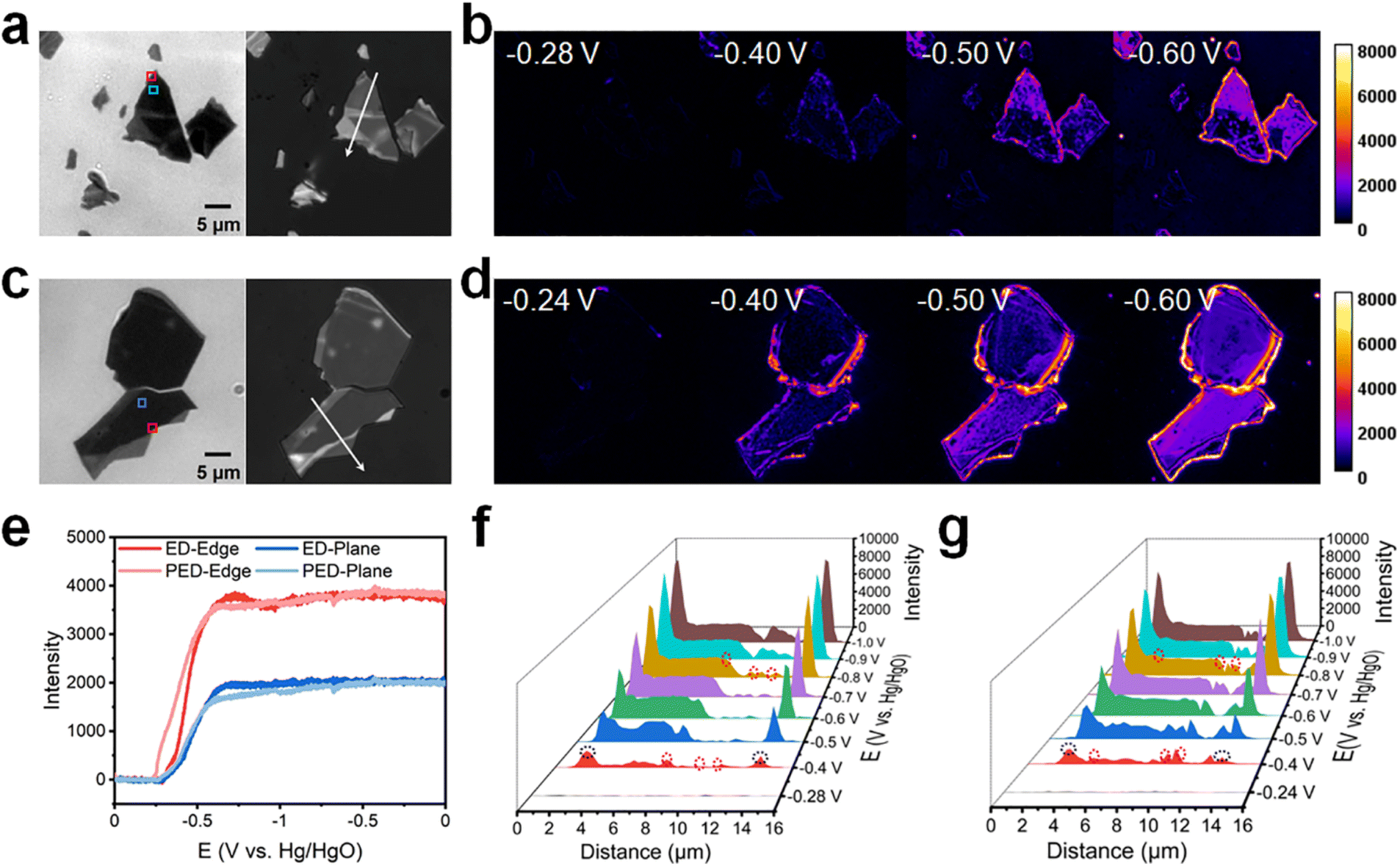 | ||
| Fig. 2 Molecular reaction imaging of (photo)electrodeposition on n-type MoS2 nanosheets in 1 M [Cu(NH3)4]SO4·xH2O (pH = 9.7). (a and c) Bright-field transmission images (left) and reflection images (right) of the MoS2 nanosheets that underwent (a) ED and (c) PED. (b) ED of MoS2 nanosheets in epi mode. (d) PED of MoS2 nanosheets in epi mode and widefield 640 nm laser irradiation to stimulate MoS2 to generate carriers. (e) Reflection intensity–potential curves of the rectangular areas marked in (a) and (c), with the red and blue boxes representing an edge and plane, respectively. (f and g) Reflection intensity profiles acquired along the white arrows in (a) and (c), respectively, at different potential (E) values. Black and red circles in (f) and (g) represent the positions of the perimeter edges and interior steps, respectively. | ||
The heterogeneity induced by mechanical exfoliation underpinned the operation of our single-nanosheet molecular reaction imaging method, which was developed to investigate the reactivity of “hot spots” for electron reduction on nanosheets via ED and PED. Cyclic voltammetry (CV) experiments were conducted to examine the Cu reduction behavior on the surface of the nanosheets in situ. To the end, the potential was swept from 0 to −1 V at 20 mV s−1 (Fig. S7†). No significant differences were observed in the CV curve shape and current in the presence or absence of laser irradiation, presumably owing to the small number of nanosheets and the limited laser irradiation range. Also, because the nanosheets are mechanically exfoliated, the obtained samples have different thicknesses (Fig. S8a†). The reflection intensity of the nanometer-thick samples could vary significantly. The reflection of the thinner regions is normally higher (area 1 in Fig. S8c,† ∼8300), and that of the thicker regions is normally lower (area 2 in Fig. S8c,† ∼5300). At the end of the reaction, we obtained the same reflection intensity (∼7400) in the deposited Cu region (Fig. S8b†). Therefore, in the process of Cu deposition, the high-intensity regions became dimmer after Cu deposition, whereas the low-intensity region brightened (Fig. S8c†).
To clearly observe the Cu deposition on the surface of the nanosheets, a “difference” operation was performed to subtract background data. Molecular reaction imaging was conducted for ED on the ITO electrode coated with n-type MoS2 nanosheets in a 1 M [Cu(NH3)4]SO4·xH2O electrolyte in epi mode (Fig. 2b). Notably, multilayer MoS2 exhibits a narrow bandgap (Eg = 1.30 eV) and thereby shows activity from the IR to UV regions.42 Furthermore, the ITO electrode is optically transparent and does not absorb photons in the visible region. Therefore, 640 nm laser irradiation was employed in this study to activate the n-type MoS2 to produce photogenerated carriers. Molecular reaction imaging was also conducted for PED on the ITO electrode coated with n-type MoS2 nanosheets in a 1 M [Cu(NH3)4]SO4·xH2O electrolyte (Fig. 2d).
Intensity–potential curves were acquired for the different regions on the surface of MoS2 during ED and PED (Fig. 2e; data extracted from Fig. 2b and d). During ED and PED, metallic Cu began to deposit at approximately −0.28 V and −0.24 V, respectively, with the difference in the onset potentials of Cu deposition being only 40 mV. Moreover, the intensity tended to stabilize at approximately −0.65 V, indicating that Cu further extended outward after being sufficiently deposited. During deposition, the intensity changes at the edges were more significant than those on the planes.
Subsequently, the Cu deposition sites were investigated to further understand the manner in which surface heterogeneity affected Cu deposition. Reflection intensity profiles corresponding to ED were acquired (Fig. 2f) along the white arrow in Fig. 2a. Initially, no deposition occurred on the nanosheets at −0.28 V. However, Cu began to nucleate as the voltage became more negative. At −0.4 V, significant deposition was observed at the perimeter edges (1.9 and 14.1 μm; black dashed circles in Fig. S6a† and 2f), with minimal deposition occurring at the interior steps (7.7, 9.3, and 10.9 μm; red dashed circles in Fig. S6a† and 2f). On the plane, the Cu nucleation sites were concentrated in the thicker regions. As the voltage became more negative, Cu grew at the nucleation sites and extended outward.
Reflection intensity profiles corresponding to PED (Fig. 2g) were acquired along the white arrow in Fig. 2c. Initially, no deposition was observed on the nanosheets at −0.24 V. However, Cu began to nucleate as the voltage became more negative. At −0.4 V, significant deposition occurred at the perimeter edges (1.9 and 13.3 μm; black dashed circles in Fig. S6b† and 2g), with minimal deposition observed at the interior steps (4.5, 9.3, and 10.7 μm; red dashed circles in Fig. S6b† and 2g). Overall, the experimental results showed that illumination had no obvious effect on n-type MoS2.
In n-type semiconductors, the concentration of electrons is higher than that of holes; therefore, the Fermi level is near the conduction band.43,44 Under illumination, the concentration of the photogenerated holes is significantly higher than the original equilibrium concentration; furthermore, the quasi-Fermi level of holes deviates more significantly from the original Fermi level, whereas that of electrons is generally near the original Fermi level.45 For the Cu deposition reaction, electrons are the charge carriers of interest. When a negative potential is applied, the holes produced under illumination pass through the external circuit to the counter electrode, whereas the electrons concentrate on the surface and participate in the surface reaction.46 Because electrons are the majority carriers in n-type semiconductors, the electron concentration does not change significantly under illumination; therefore, the onset potential of Cu deposition does not show a significant positive shift. Additionally, when Cu is deposited on the surface of MoS2, it tends to nucleate at the perimeter edges and interior steps first and then nucleate at a more negative voltage on the thicker plane. This action mechanism is consistent with that reported previously.37,40,47
(Photo)electrodeposition on p-type WSe2
To gain deeper insights into the effects of surface heterogeneity on the Cu deposition, further studies were conducted using p-type WSe2 nanosheets, which were prepared in the same manner as MoS2 (mechanical exfoliation from crystals using low-residue Nitto tape; see Fig. S3† for additional images). The transmission and reflection intensities of p-type WSe2 showed a correlation (Fig. S9†), indicating that regions with high transmission intensity also exhibited high reflection intensity. Moreover, the variation in the reflection intensity was more pronounced than that in the transmission intensity, enabling a better distinction between edges and planes.Subsequently, molecular reaction imaging was conducted for ED and PED on the p-type WSe2 nanosheets in epi mode (Fig. 3b and d). Owing to the narrow bandgap of multilayer WSe2 (Eg = 1.25 eV),48 640 nm laser irradiation was employed to activate p-type WSe2 to produce photogenerated carriers. In the CV experiments, the potential was swept from 0.4 to −0.6 V at 20 mV s−1 (Fig. S10†). Furthermore, intensity–potential curves were acquired for different regions on the surface of WSe2 during ED and PED (Fig. 3e; data extracted from Fig. 3b and d).
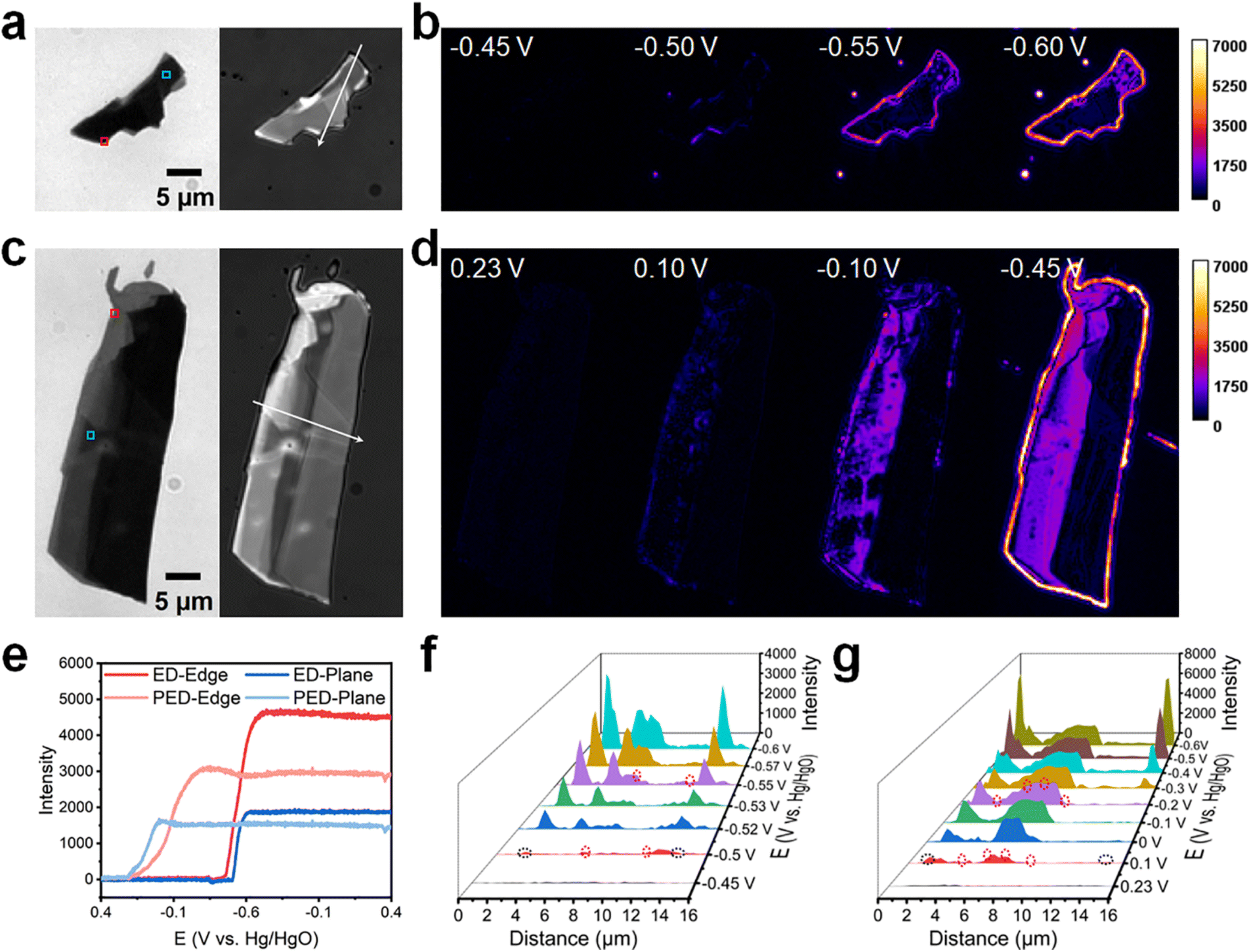 | ||
| Fig. 3 Molecular reaction imaging of (photo)electrodeposition on p-type WSe2 nanosheets in 1 M [Cu(NH3)4]SO4·xH2O (pH = 9.7). (a and c) Bright-field transmission images (left) and reflection images (right) of the WSe2 nanosheets that underwent (a) ED and (c) PED. (b) Electrodeposition of WSe2 nanosheets in epi mode. (d) Photoelectrodeposition of WSe2 nanosheets in epi mode and widefield 640 nm laser irradiation for stimulating WSe2 to generate carriers. (e) Reflection intensity–potential curves of the rectangular areas marked in (a) and (c), with the red and blue boxes representing an edge and plane, respectively. (f and g) Reflection intensity profiles acquired along the white arrows in (a) and (c), respectively, at different E values; black and red circles represent positions of the perimeter edges and interior steps, respectively. | ||
In ED, metallic Cu began to deposit at approximately −0.45 V, a more negative value than that observed for n-type MoS2. Additionally, deposition at the edge occurred 50 mV earlier than that on the plane. The intensity changed rapidly but did not stabilize at the vertex potential of −0.6 V; however, it settled at approximately −0.56 V upon sweep reversal at −0.6 V. In PED, metallic Cu began to deposit at ∼0.23 V; therefore, the difference in the onset potentials of Cu deposition was 680 mV. Moreover, the intensity at the plane and edge tended to stabilize within 250 mV and 550 mV, respectively. In the presence of laser irradiation, the growth rate of Cu on the plane exceeded that at the edge. Notably, the intensity change at the edge during deposition was more significant than that on the plane, similar to that of MoS2.
To directly observe Cu deposition on the sample surface, reflection intensity profiles were acquired along the white arrows shown in Fig. 3a and c for ED and PED (Fig. 3f and g). In ED, no deposition was initially observed on the nanosheets at −0.45 V. However, Cu nucleation began as the voltage became more negative. At −0.5 V, moderate deposition occurred at the perimeter edges (1.6 and 13.3 μm; black dashed circles in Fig. S9a† and 3f) and interior steps (6.9 and 11.5 μm; red dashed circles in Fig. S9a† and 3f). Concurrently, Cu began to deposit on the plane, with nucleation sites concentrated in the thicker regions. In PED, significant deposition occurred at 0.1 V at the perimeter edges (1.3 and 15.2 μm; black dashed circles in Fig. S9b† and 3g) and interior steps (3.7, 5.9, 7.1 and 8.7 μm; red dashed circles in Fig. S9b† and 3g). The intensity changed significantly faster on the plane than at the edge. At 0 V, the intensity in the 4.8–8.8 μm region appeared to be higher than that in the 1–2 μm zone. Moreover, the intensity in the 4.8–8.8 μm region showed no significant change after −0.1 V, whereas that in the 1–2 μm zone increased until −0.6 V. Cu growth ceased once the deposition site on the plane was covered, whereas deposition continued on the deposited metallic Cu at the perimeter edge, enabling a relatively high-resolution assessment of electron distribution (∼0.35 μm; Fig. S11†).
Furthermore, electron transfer on the WSe2 surface was investigated using a focused laser spot at a wavelength of 640 nm, and the laser spot diameter was 0.64 μm. To the end, bright-field transmission and reflection images of WSe2 were acquired (Fig. 4a; see Fig. 4a(iii) for the image of the focused laser spot); moreover, the Cu deposition on the nanosheets was analyzed when the focused laser spot was aimed at different sample locations (white crosses in Fig. 4b). In these experiments, a linear sweep voltammetric (LSV) potential was applied from 0.4 V to −0.1 V at 5 mV s−1 and the focused laser density was set at 10 kW cm−2. Under these conditions, neither electricity nor laser irradiation enabled Cu deposition on the surface of WSe2. Nevertheless, Cu was preferentially deposited at an active site near the focused laser spot, indicating limited transport possibly because of electron capture by defects or electron consumption by recombination with holes during transport.9
 | ||
| Fig. 4 Molecular reaction imaging of PED on p-type WSe2 nanosheets with focused laser irradiation in 1 M [Cu(NH3)4]SO4·xH2O (pH = 9.7). (a) Bright field transmission (i) and reflection images (ii) of the WSe2 nanosheets, with an image of the focused laser spot (iii). (b) PED of WSe2 nanosheets in epi mode and 640 nm focused laser irradiation for stimulating WSe2 to generate carriers. White dashed lines represent the nanosheet contour and interior steps. White crosses represent the laser-targeted locations. Orange circles represent certain deposition locations away from the laser location-targeted areas. | ||
However, a few electrons traveled to locations far from the laser-targeted areas (orange circles in Fig. 4b). Photogenerated electrons moved tens of microns in a manner parallel to the layers from the carrier generating sites to the reactive hot spots; this distance is smaller than that reported by Samber and co-workers (45 μm).37 Additionally, the onset potential of Cu deposition fluctuated with changes in the laser spot positioning. When the laser spot was aimed at a location (such as the white cross in Fig. 4b(iii)), Cu precipitation occurred at ∼0.36 V; however, when it was directed at other sites (such as the white cross in Fig. 4b(v)), Cu started to deposit minimally at ∼0.05 V, suggesting the uneven distribution of WSe2 surface-active sites. Focused laser spots can induce high local catalytic activity owing to localized carrier injection;49 however, this deviates from the actual working conditions and can therefore only guide studies on material modification. In contrast, widefield laser irradiation is more suitable for evaluating the overall nanosheet activity in operando.
For p-type semiconductors, in which the hole concentration surpasses the electron concentration, the Fermi level is close to the valence band.43,44 In the absence of light, electrons cannot readily transition to the conduction band, hindering further redox reactions on the surface. Consequently, the onset potential of p-type WSe2 during ED is more negative than that of n-type MoS2. However, under illumination, the concentration of the photogenerated electrons significantly exceeds the original equilibrium concentration, causing a substantial deviation of the quasi-Fermi level of electrons from the original Fermi level. Furthermore, the quasi-Fermi level of holes typically remains near the original Fermi level.45
As mentioned earlier, electrons serve as charge carriers during Cu deposition reaction. When a negative potential is applied, the holes produced under illumination traverse the external circuit to the counter electrode, while electrons accumulate on the surface and participate in surface reactions.46 Because electrons are the minority carriers in p-type semiconductors, their concentration varies significantly under illumination, leading to the noteworthy positive shift (680 mV) in the onset potential of Cu deposition observed in this study. The incident photons under laser action facilitate the formation of new active sites on the surface of WSe2 owing to the incident photon, thereby generating additional electrons for Cu reduction, leading to a higher growth rate of Cu on the plane than that at the perimeter edge.50
Subsequently, the effects of laser density were investigated (Fig. 5) by varying the illumination density from 0 to 0.25 kW cm−2, and conducting molecular reaction imaging of the Cu reduction reaction. According to the results, the onset potential (Eon) of Cu deposition on n-type MoS2 (red curve in Fig. 5) increased slightly with increasing laser density, shifting from −0.30 V at 0 kW cm−2 to −0.26 V at 0.25 kW cm−2 (see Fig. S12† for detailed molecular reaction imaging data acquired at different laser densities). However, the Eon value of Cu deposited on p-type WSe2 (black curve) shifted positively with increasing laser density, transitioning from −0.43 V at 0 kW cm−2 to 0.23 V at 0.1 kW cm−2. Notably, Eon experienced only a slight positive shift when the laser power exceeded 0.1 kW cm−2 (from 0.23 V at 0.1 kW cm−2 to 0.27 V at 0.25 kW cm−2; see Fig. S13† for detailed molecular reaction imaging data obtained at different laser densities). The significant effect of the laser density stemmed from its ability to regulate the electron density.51 As the light intensity increased, the carrier concentration saturated, resulting in no notable shift in Eon with a further increase in the light intensity.52
 | ||
| Fig. 5 Influence of laser density on onset potential (Eon) of Cu deposition on two different nanosheets. | ||
When a semiconductor is subjected to laser irradiation, the photogenerated carriers influence band bending at the semiconductor-solution interface, consequently affecting the open-circuit potential (Voc).53 Therefore, the response of Voc to light intensity was examined (Fig. S14†). Notably, the Voc of n-type MoS2 exhibited insignificant changes with respect to the light intensity, whereas that of p-type WSe2 showed a positive shift. Additionally, the Voc of the ITO substrate in the electrolyte remained unchanged as the light intensity was varied. Specifically, the Voc of p-type WSe2 underwent a positive shift from 0.39 V at 0 kW cm−2 to 0.54 V at 0.1 kW cm−2. However, this shift was minimal when the laser density exceeded 0.1 kW cm−2 (from 0.54 V at 0.1 kW cm−2 to 0.58 V at 0.25 kW cm−2). Importantly, when the laser was deactivated, Voc rapidly returned to ∼0.38 V. Conversely, for n-type MoS2, Voc only experienced a 10 mV change after laser irradiation. These results agree with the changes observed in Eon with varying light intensity.
Active site mapping via chemical deposition
To further investigate the influence of illumination on the semiconductor surface, HAuCl4 was used as an oxidant to characterize the redox-active sites of the semiconductor. HAuCl4 has been extensively used as a molecular probe to map chemically active sites.54–56 The Fermi levels of MoS2 and WSe2 are reportedly 4.6–4.9 eV below the vacuum level.57 Moreover, at 0 pH and 1 atm hydrogen pressure, ERHE has been estimated to be 4.43–4.47 eV below the vacuum level.58 Additionally, the reduction potential of AuCl4− (AuCl4− + 3e− = Au0 + 4Cl−) is +1.002 V vs. the standard hydrogen electrode (SHE) potential. Thus, electrons in the nanosheets may spontaneously shift to HAuCl4 to reduce it to metallic Au0 particles while oxidizing themselves to soluble species in the aqueous solution, as expressed below.59| 6AuCl4− + MoS2 + 12H2O = 6Au0 + MoO42− + 2SO42− + 24Cl− + 24H+ | (2) |
| 6AuCl4− + WSe2 + 12H2O = 6Au0 + WO42− + 2SeO42− + 24Cl− + 24H+ | (3) |
In the present study, the same nanosheet was used for ED, PED and chemical deposition. To eliminate the influence of light on the surface of the nanosheets, ED was first performed, followed by the complete dissolution of the deposited metallic Cu in accordance with reaction (S4),† which was evidently achieved within ∼5 min (Fig. S15†). Subsequently, PED was performed on the same nanosheet and the deposited metallic Cu was dissolved using the method described above. Finally, the redox sites on the nanosheets were characterized by chemical deposition. In this study, chemical reduction of HAuCl4 was monitored in trans-illumination mode to obtain a better contrast. The “difference” operation was conducted to subtract background data, thus permitting relatively unimpeded observation of the deposition sites.
Molecular reaction imaging was performed for ED, PED, and chemical deposition on the same n-type MoS2 nanosheet (Fig. 6), and the corresponding bright-field transmission and reflection images of the MoS2 nanosheets were acquired (Fig. S16a†). The results revealed that no significant differences in the distribution of the Cu deposition sites under dark and laser illumination conditions. The nucleation sites were primarily concentrated at the perimeter edges and interior steps and evenly distributed on the plane (Fig. 6d and e). As time progressed, the deposited Cu nanoparticles grew at the nucleation sites, and the coverage area of Cu on the semiconductor surface increased. However, in the chemical deposition experiments (Fig. 6c and f), Au particles were deposited only at the perimeter edge of the nanosheet, indicating that the redox sites on the surface of MoS2 existed only at the perimeter edge. Cu deposition on the surface during ED and PED was likely influenced by the electrocatalytic activation of certain low-activity sites on the surface, whereas the laser irradiation did not have a significant catalytic effect on n-type MoS2.
 | ||
| Fig. 6 Molecular reaction imaging of n-type MoS2 nanosheets. (a) ED at a constant potential of −0.4 V. (b) PED at a constant potential of −0.4 V and laser density of 0.25 kW cm−2. (c) Chemical deposition in the absence of electricity and laser irradiation. (d–f) Reflection intensity profiles acquired at different durations along the white arrows shown in (a–c). Purple curve in (d) represents the reflection intensity of the primary reflection image shown in Fig. S16.† Black and red circles/dashed lines represent positions of the perimeter edges and interior steps, respectively. Scale bar: 1 μm. | ||
Molecular reaction imaging was also performed for ED, PED, and chemical deposition on the same p-type WSe2 nanosheet (Fig. 7), and the corresponding bright-field transmission and reflection images were acquired (Fig. S16b†). The Cu electrodeposited on WSe2 at a constant potential of −0.6 V mainly concentrated at the perimeter edges and interior steps in a linear manner (dashed white lines in Fig. 7a). Because the deposition potential of Cu shifted significantly in the presence of laser irradiation, PED was conducted at −0.1 V (Fig. 7b). The results indicated that the nucleation sites of Cu were mainly located in the plane, with a few nucleation sites present at the perimeter edge, thereby exhibiting a point-like distribution. After dissolving metallic Cu, chemical deposition was performed on the same nanosheet (Fig. 7c). Au particles were deposited not only at the perimeter edge and the interior step of the nanosheet but also on the plane of the nanosheet, suggesting that the active sites of the electrocatalytic and photoelectrocatalytic redox reactions were combined.
 | ||
| Fig. 7 Molecular reaction imaging of p-type WSe2 nanosheets. (a) ED at a constant potential of −0.6 V. (b) PED at a constant potential of −0.1 V and laser density of 0.25 kW cm−2. (c) Chemical deposition in the absence of electricity and laser irradiation. White dashed lines represent interior steps. (d–f) Reflection intensity profiles acquired at different durations along the white arrows shown in (a–c). Purple curve in (d) denotes the reflection intensity of the primary reflection image shown in Fig. S16.† Black and red circles/dashed lines represent positions of the perimeter edges and interior steps, respectively. Blue spots/dashed lines denote positions of the plane. Scale bar: 1 μm. | ||
The obtained reflection intensity profiles suggested that the peak intensities corresponding to the ED and PED were always complementary (Fig. 7d and e). Additionally, chemical deposition presumably occurred at the active sites of ED and PED (Fig. 7f). For example, at the interior steps (2.4, 4.2, and 8.7 μm; red dashed lines in Fig. 7d–f), the highest and lowest intensities were observed during ED and PED, respectively. Conversely, at the plane (3.7, 6.8 μm; blue dashed lines in Fig. 7d–f), an intensity change was observed during PED but not during ED. Furthermore, at the aforementioned locations, significant intensity changes occurred during chemical deposition. This was probably due to the laser laser-irradiation-induced generation of more new active sites on the surface of WSe2, resulting in a higher more charge for Cu reduction. Consequently, the distribution of Cu nanoparticles on the surface of the semiconductors differed from each other.50
Conclusion
An optical imaging strategy was developed to visualize the dynamic distribution of electron-transferring active sites on narrow-bandgap semiconductors in situ in different catalytic processes using metal deposition as the reporting mechanism. In this approach, n-type MoS2 and p-type WSe2 showed different responses in electrocatalytic and photoelectrocatalytic processes. For n-type MoS2, a high electron concentration diminished the difference between scenarios with and without illumination. For p-type WSe2, in which electrons were the minority carriers, the limited activation sites concentrated at the steps and edges in the electrocatalytic process. In the presence of light, the photogenerated electrons significantly shifted the reaction onset potential in a positive direction, producing more active sites with a uniform distribution on the WSe2 plane. Thus, an interesting complementary pattern was discovered for different processes. This simple, versatile analytical approach opens a new path for comprehensively clarifying the heterogeneous structure–property relationships of various electrocatalytic and photoelectrocatalytic materials, which could further aid the rational design of high-performance catalytic devices.Data availability
The experimental procedures and data are provided in the ESI.†Author contributions
R. H. conceived and supervised the project. L. W. and H. C. performed the experiments. L. W. and R. H. wrote the manuscript.Conflicts of interest
There are no conflicts to declare.Acknowledgements
We gratefully acknowledge financial support from the National Natural Science Foundation of China (22074059 and 22374064) and the Shenzhen Innovation of Science and Technology Commission (ZDSYS20230626090803004).References
- G. Li, D. Zhang, Q. Qiao, Y. Yu, D. Peterson, A. Zafar, R. Kumar, S. Curtarolo, F. Hunte, S. Shannon, Y. Zhu, W. Yang and L. Cao, All the catalytic active sites of MoS2 for hydrogen evolution, J. Am. Chem. Soc., 2016, 138, 16632–16638 CrossRef CAS PubMed.
- X. Li, T. Li, Y. Ma, Q. Wei, W. Qiu, H. Guo, X. Shi, P. Zhang, A. M. Asiri, L. Chen, B. Tang and X. Sun, Boosted electrocatalytic N2 reduction to NH3 by defect-rich MoS2 nanoflower, Adv. Energy Mater., 2018, 8, 1801357 CrossRef.
- J. Hu, L. Yu, J. Deng, Y. Wang, K. Cheng, C. Ma, Q. Zhang, W. Wen, S. Yu, Y. Pan, J. Yang, H. Ma, F. Qi, Y. Wang, Y. Zheng, M. Chen, R. Huang, S. Zhang, Z. Zhao, J. Mao, X. Meng, Q. Ji, G. Hou, X. Han, X. Bao, Y. Wang and D. Deng, Sulfur vacancy-rich MoS2 as a catalyst for the hydrogenation of CO2 to methanol, Nat. Catal., 2021, 4, 242–250 CrossRef CAS.
- B. M. Weckhuysen, Chemical imaging of spatial heterogeneities in catalytic solids at different length and time scales, Angew. Chem., Int. Ed., 2009, 48, 4910–4943 CrossRef CAS.
- J. W. Hill and C. M. Hill, Directly mapping photoelectrochemical behavior within individual transition metal dichalcogenide nanosheets, Nano Lett., 2019, 19, 5710–5716 Search PubMed.
- S. Sarkar, X. Wang, M. Hesari, P. Chen and M. V. Mirkin, Scanning electrochemical and photoelectrochemical microscopy on finder grids: toward correlative multitechnique imaging of surfaces, Anal. Chem., 2021, 93, 5377–5382 Search PubMed.
- X. Yu, N. Guijarro, M. Johnson and K. Sivula, Defect mitigation of solution-processed 2D WSe2 nanoflakes for solar-to-hydrogen conversion, Nano Lett., 2018, 18, 215–222 CrossRef CAS PubMed.
- Y. Sun, X. Zhang, B. Mao and M. Cao, Controllable selenium vacancy engineering in basal planes of mechanically exfoliated WSe2 monolayer nanosheets for efficient electrocatalytic hydrogen evolution, Chem. Commun., 2016, 52, 14266–14269 RSC.
- Z. Nilsson, M. Van Erdewyk, L. Wang and J. B. Sambur, Molecular reaction imaging of single-entity photoelectrodes, ACS Energy Lett., 2020, 5, 1474–1486 CrossRef CAS.
- R. Xie, J. Gao, S. Wang, H. Li and W. Wang, Optically imaging in situ effects of electrochemical cycling on single nanoparticle electrocatalysis, Anal. Chem., 2024, 96, 2455–2463 Search PubMed.
- C. Jing, F. J. Rawson, H. Zhou, X. Shi, W. Li, D. Li and Y. Long, New insights into electrocatalysis based on plasmon resonance for the real-time monitoring of catalytic events on single gold nanorods, Anal. Chem., 2014, 86, 5513–5518 Search PubMed.
- C. L. Bentley, J. Edmondson, G. N. Meloni, D. Perry, V. Shkirskiy and P. R. Unwin, Nanoscale electrochemical mapping, Anal. Chem., 2019, 91, 84–108 CrossRef CAS.
- M. Saqib, Y. Fan, R. Hao and B. Zhang, Optical imaging of nanoscale electrochemical interfaces in energy applications, Nano Energy, 2021, 90, 106539 CrossRef CAS.
- L. Jean-François, H. Wang, W. Wang and F. Kanoufi, Emerging optical microscopy techniques for electrochemistry, Annu. Rev. Anal. Chem., 2021, 15, 57–82 Search PubMed.
- C. L. Tolbert and C. M. Hill, Electrochemically probing exciton transport in monolayers of two-dimensional semiconductors, Faraday Discuss., 2022, 233, 163–174 Search PubMed.
- M. Ju, R. Cai, J. Ren, J. Chen, L. Qi, X. Long and S. Yang, Conductive polymer intercalation tunes charge transfer and sorption–desorption properties of LDH enabling efficient alkaline water oxidation, ACS Appl. Mater. Interfaces, 2021, 13, 37063–37070 Search PubMed.
- M. V. Erdewyk and J. B. Sambur, Single nanoflake photoelectrochemistry reveals intrananoflake doping heterogeneity that explains ensemble-level photoelectrochemical behavior, ACS Appl. Mater. Interfaces, 2022, 14, 22737–22746 CrossRef CAS.
- R. Hao, Y. Fan, M. D. Howard, J. C. Vaughan and B. Zhang, Imaging nanobubble nucleation and hydrogen spillover during electrocatalytic water splitting, Proc. Natl. Acad. Sci. U. S. A., 2018, 115, 5878–5883 Search PubMed.
- R. Hao, Y. Fan, T. J. Anderson and B. Zhang, Imaging single nanobubbles of H2 and O2 during the overall water electrolysis with single-molecule fluorescence microscopy, Anal. Chem., 2020, 92, 3682–3688 CrossRef CAS.
- W. Wang, J. Chen, Z. Lou, S. Kim, M. Fujitsuka, H. Yu and T. Majima, Single-molecule and -particle probing crystal edge/corner as highly efficient photocatalytic sites on a single TiO2 particle, Proc. Natl. Acad. Sci. U. S. A., 2019, 116, 18827–18833 CrossRef CAS.
- X. Zhao, Y. Li, Y. Cui, M. Saqib, X. Zhang, R. Hao and Z. Zheng, Spatiotemporally and chemically resolved imaging of electrocatalytic oxygen evolution on single nanoplates of cobalt-layered hydroxide, J. Am. Chem. Soc., 2023, 145, 20897–20906 CrossRef CAS.
- M. Chen, W. Zhao, M. Zhu, X. Li, C. Xu, H. Chen and J. Xu, Spatiotemporal imaging of electrocatalytic activity on single 2D gold nanoplates via electrogenerated chemiluminescence microscopy, Chem. Sci., 2019, 10, 4141–4147 RSC.
- C. Ma, W. Wu, L. Li, S. Wu, J. Zhang, Z. Chen and J. Zhu, Dynamically imaging collision electrochemistry of single electrochemiluminescence nano-emitters, Chem. Sci., 2018, 9, 6167–6175 RSC.
- Y. Chen, D. Zhao, J. Fu, X. Gou, D. Jiang, H. Dong and J. J. Zhu, In situ imaging facet-induced spatial heterogeneity of electrocatalytic reaction activity at the subparticle level via electrochemiluminescence microscopy, Anal. Chem., 2019, 91, 6829–6835 CrossRef CAS PubMed.
- Y. Wang, Y. Jiang and W. Wang, Determining the subnanometer thickness of the water-depletion layer at the interface between water and the hydrophobic substrate, Anal. Chem., 2019, 91, 11696–11702 CrossRef CAS.
- Y. Wang, X. Shan, H. Wang, S. Wang and N. Tao, Plasmonic imaging of surface electrochemical reactions of single gold nanowires, J. Am. Chem. Soc., 2017, 139, 1376–1379 CrossRef CAS PubMed.
- S. Hu, J. Yi, Y. Zhang, K. Lin, B. Liu, L. Chen, C. Zhan, Z. Lei, J. Sun, C. Zong, J. Li and B. Ren, Observing atomic layer electrodeposition on single nanocrystals surface by dark field spectroscopy, Nat. Commun., 2020, 11, 2518 CrossRef CAS.
- S. Xu, X. Yu, Z. Chen, Y. Zeng, L. Guo, L. Li, F. Luo, J. Wang, B. Qiu and Z. Lin, Real-time visualization of the single-nanoparticle electrocatalytic hydrogen generation process and activity under dark field microscopy, Anal. Chem., 2020, 92, 9016–9023 CrossRef CAS.
- X. Zhao, H. Chen, Y. Cui, X. Zhang and R. Hao, Dual-mode imaging of dynamic interaction between bubbles and single nanoplates during the electrocatalytic hydrogen evolution process, Small, 2024, 20, 2400273 CrossRef CAS.
- R. C. Evans, Z. Nilsson, B. Balch, L. Wang, J. R. Neilson, C. R. Weinberger and J. B. Sambur, Quantifying capacitive-like and battery-like charge storage contributions using single-nanoparticle electro-optical imaging, ChemElectroChem, 2020, 7, 753–760 CrossRef CAS.
- S. Redor, L. Godeffroy, G. Rousse, A. M. Abakumov, B. Li, F. Kanoufi and J.-M. Tarascon, Electrochromic corundum-like compound based on the reversible (de)insertion of lithium: Li2Ni2W2O9, J. Am. Chem. Soc., 2023, 145, 12823–12836 CrossRef CAS PubMed.
- J. Mao, G. Li, D. Xu and R. Hao, Direct imaging of dynamic heterogeneous lithium–gold interaction at the electrochemical interface during the charging/discharging processes, Chem. Sci., 2024, 15, 3192–3202 RSC.
- M. D. Kelzenberg, D. B. Turner-Evans, B. M. Kayes, M. A. Filler, M. C. Putnam, N. S. Lewis and H. A. Atwater, Photovoltaic measurements in single-nanowire silicon solar cells, Nano Lett., 2008, 8, 710–714 Search PubMed.
- R. Li, F. Zhang, D. Wang, J. Yang, M. Li, J. Zhu, X. Zhou, H. Han and C. Li, Spatial separation of photogenerated electrons and holes among {010} and {110} crystal facets of BiVO4, Nat. Commun., 2013, 4, 1432 Search PubMed.
- A. E. Isenberg, M. A. Todt, L. Wang and J. B. Sambur, Role of photogenerated iodine on the energy-conversion properties of MoSe2 nanoflake liquid junction photovoltaics, ACS Appl. Mater. Interfaces, 2018, 10, 27780–27786 CrossRef CAS.
- M. A. Todt, A. E. Isenberg, S. U. Nanayakkara, E. M. Miller and J. B. Sambur, Single-nanoflake photo-electrochemistry reveals champion and spectator flakes in exfoliated MoSe2 films, J. Phys. Chem. C, 2018, 122, 6539–6545 CrossRef CAS.
- M. V. Erdewyk and J. B. Sambur, Molecular reaction imaging of a surface recombination process explains performance variation among smooth MoS2 photoelectrodes, J. Electrochem. Soc., 2022, 169, 096519 CrossRef.
- J. B. Sambur, T. Chen, E. Choudhary, G. Chen, E. J. Nissen, E. M. Thomas, N. Zou and P. Chen, Sub-particle reaction and photocurrent mapping to optimize catalyst-modified photoanodes, Nature, 2016, 530, 77–80 CrossRef CAS.
- X. Mao and P. Chen, Inter-facet junction effects on particulate photoelectrodes, Nat. Mater., 2022, 21, 331–337 CrossRef CAS.
- T. Huang, B. Dong, S. L. Filbrun, A. A. Okmi, X. Cheng, M. Yang, N. Mansour, S. Lei and N. Fang, Single-molecule photocatalytic dynamics at individual defects in two-dimensional layered materials, Sci. Adv., 2021, 7, eabj4452 CrossRef CAS.
- K. Kawashima, R. A. Márquez, Y. J. Son, C. Guo, R. R. Vaidyula, L. A. Smith, C. E. Chukwuneke and C. B. Mullins, Accurate potentials of Hg/HgO electrodes: practical parameters for reporting alkaline water electrolysis overpotentials, ACS Catal., 2023, 13, 1893–1898 CrossRef CAS.
- C.-P. Lu, G. Li, J. Mao, L. Wang and E. Y. Andrei, Bandgap, mid-gap states, and gating effects in MoS2, Nano Lett., 2014, 14, 4628–4633 CrossRef CAS PubMed.
- D. de Cogan, in Solid State Devices: A Quantum Physics Approach, ed. D. de Cogan, Macmillan Education UK, London, 1987, pp. 77–92, DOI:10.1007/978-1-349-18658-7_5.
- M. Evstigneev, in Introduction to Semiconductor Physics and Devices, ed. M. Evstigneev, Springer International Publishing, Cham, 2022, pp. 151–170, DOI:10.1007/978-3-031-08458-4_6.
- M. Z. Rahman, T. Edvinsson and J. Gascon, Hole utilization in solar hydrogen production, Nat. Rev. Chem, 2022, 6, 243–258 CrossRef PubMed.
- C. Cheng, W. Zhang, X. Chen, S. Peng and Y. Li, Strategies for improving photoelectrochemical water splitting performance of Si-based electrodes, Energy Sci. Eng., 2022, 10, 1526–1543 CrossRef CAS.
- R. J. Castro and C. R. Cabrera, Photoelelctrochemistry and surface studies of copper interaction with rough surfaces of p-MoSe2, J. Electrochem. Soc., 1992, 139, 3385–3390 CrossRef CAS.
- Q. Cheng, J. Pang, D. Sun, J. Wang, S. Zhang, F. Liu, Y. Chen, R. Yang, N. Liang, X. Lu, Y. Ji, J. Wang, C. Zhang, Y. Sang, H. Liu and W. Zhou, WSe2 2D p-type semiconductor-based electronic devices for information technology: Design, preparation, and applications, InfoMat, 2020, 2, 656–697 CrossRef CAS.
- D. V. Esposito, J. B. Baxter, J. John, N. S. Lewis, T. P. Moffat, T. Ogitsu, G. D. O'Neil, T. A. Pham, A. A. Talin, J. M. Velazquez and B. C. Wood, Methods of photoelectrode characterization with high spatial and temporal resolution, Energy Environ. Sci., 2015, 8, 2863–2885 RSC.
- M. V. d. L. Tinoco, M. B. Costa, L. H. Mascaro and J. F. de Brito, Photoelectrodeposition of Pt nanoparticles on Sb2Se3 photocathodes for enhanced water splitting, Electrochim. Acta, 2021, 382, 138290 CrossRef CAS.
- J. Yu, H. Saada, R. Abdallah, G. Loget and N. Sojic, Luminescence amplification at BiVO4 photoanodes by photoinduced electrochemiluminescence, Angew. Chem., Int. Ed., 2020, 59, 15157–15160 CrossRef CAS.
- R. Chen, D. Zhang, Z. Wang, D. Li, L. Zhang, X. Wang, F. Fan and C. Li, Linking the photoinduced surface potential difference to interfacial charge transfer in photoelectrocatalytic water oxidation, J. Am. Chem. Soc., 2023, 145, 4667–4674 CrossRef CAS PubMed.
- S. Solak, P. W. M. Blom and G. A. H. Wetzelaer, Effect of non-ohmic contacts on the light-intensity dependence of the open-circuit voltage in organic solar cells, Appl. Phys. Lett., 2016, 109, 053302 CrossRef.
- Z. Wang, A. Sim, J. J. Urban and B. Mi, Removal and recovery of heavy metal ions by two-dimensional MoS2 nanosheets: performance and mechanisms, Environ. Sci. Technol., 2018, 52, 9741–9748 CrossRef CAS.
- Y. Yuan, W. Zhan, F. Jia, S. Song and A. López-Valdivieso, The reduction mechanism of HAuCl4 on the surface of edge-rich molybdenum disulfide, Surf. Interfaces, 2022, 33, 102199 CrossRef CAS.
- Y. Yuan, B. Yang, F. Jia and S. Song, Reduction mechanism of Au metal ions into Au nanoparticles on molybdenum disulfide, Nanoscale, 2019, 11, 9488–9497 RSC.
- L. Liu, N. Xu, Y. Ke, H. Chen, Y. Zhang and S. Deng, Sensing by surface work function modulation: high performance gas sensing using van der Waals stacked bipolar junction transistor, Sens. Actuators, B, 2021, 345, 130340 CrossRef CAS.
- H. Reiss and A. Heller, The absolute potential of the standard hydrogen electrode: a new estimate, J. Phys. Chem., 1985, 89, 4207–4213 CrossRef CAS.
- A. Y. Polyakov, L. Yadgarov, R. Popovitz-Biro, V. A. Lebedev, I. Pinkas, R. Rosentsveig, Y. Feldman, A. E. Goldt, E. A. Goodilin and R. Tenne, Decoration of WS2 nanotubes and fullerene-like MoS2 with gold nanoparticles, J. Phys. Chem. C, 2014, 118, 2161–2169 CrossRef CAS.
Footnote |
| † Electronic supplementary information (ESI) available. See DOI: https://doi.org/10.1039/d4sc03640a |
| This journal is © The Royal Society of Chemistry 2024 |