DOI:
10.1039/D4SC02339K
(Edge Article)
Chem. Sci., 2024,
15, 9630-9640
Engineered solid-state aggregates in brickwork stacks of n-type organic semiconductors: a way to achieve high electron mobility†
Received
9th April 2024
, Accepted 16th May 2024
First published on 28th May 2024
Abstract
Efficient, economically viable n-type organic semiconductor materials suitable for solution-processed OFET devices with high electron mobility and ambient stability are scarce. Merging these attributes into a single molecule remains a significant challenge and a careful molecular design is needed. To address this, synthetic viability (achievable in fewer than three steps) and using cost-effective starting materials are crucial. Our research presents a strategy that meets these criteria using naphthalene diimide (NDI) core structures. The approach involves a simple synthesis process with a cost of $ 5–10 per gram for the final products. This paper highlights our success in scaling up the production using affordable known reagents, creating ambient condition solution-processed OFET devices with impressive electron mobility, on–off current ratio (1 cm2 V−1 s−1 and Ion/Ioff ∼ 109) and good ambient stability (more than 100 h). We conducted a comprehensive study on EHNDIBr2, a material that demonstrates superior performance due to its unique supramolecular arrangement in its brickwork stack. This was compared with two similar structures to validate our findings. The superior performance of EHNDIBr2 is attributed to the effective interlocking of charge-hopping units within the NDI core in its brickwork stack. Our findings include detailed electronic, spectroscopic, and microscopic analyses of these layers.
Introduction
In the past decade, significant progress has been made in developing n-type molecular semiconductors with efficient charge transport properties.1 Due to the possibility of diversifying molecular features and obtaining the desired functional outcome suitable for various electronic devices, immense efforts have been made towards developing new materials.2–6 Apart from focusing on molecular features, their solid-state packing and supramolecular structures are equally significant in deciding their charge transport properties.7–10 In the supramolecular arrangement, the relative position and magnitude of molecular displacement immensely influence (i) the intermolecular frontier molecular orbital overlap, (ii) the electronic structure and state energies, and (iii), thereby, the bulk charge carrier transport. Such interconnected complex parameters in the supramolecular structure necessitate tedious effort to unravel their roles in charge transport. From the point of view of molecular packing, widely recognized promising molecular packing motifs for efficient carrier transport include herringbone and a brickwork structure.10,11
Molecular aggregates formed by weak intermolecular interactions would yield mechanically flexible active layers and devices.12,13a,b The intrinsic solubility and processibility of such materials are also eventually determined by such non-covalent interactions. In many cases, such strong and cooperative interactions adversely affect the processibility. Hence, it is highly recommended to have a balance to achieve such conflicting requirements, and it is essential to address these non-covalent interactions at the molecular level and tailor them to obtain the desired materials with suitable carrier transport.13c Additionally, in systems with poorly managed molecular ordering due to the lack of appropriate functional groups to benefit such non-covalent interactions, thermally induced lattice vibrations and, thereby, lowering of charge carrier transport are well known. Hence, reduction of dynamic disorder by engineered supramolecular lattice assembly and crystalline active layers are essential to achieve high performance in semiconductor devices. There are some recent reports in the abovementioned directions.14–18 Some molecular semiconductors and OFETs derived from them have exhibited benchmark performance in laboratory scale devices. Most of them fall into p-type materials.19–22 N-type materials developed by an easy synthetic strategy and less expensive chemicals are essential for the mass production and wide use of such materials. Hence, our comprehensive approach to tackle most of these requirements is summarized here. Complex electron-deficient backbones are purposefully excluded from the molecular design due to the complex synthetic routes that limit the scalability. Special attention was devoted to designing the molecular structure to yield multiple intermolecular solid-state interactions to minimize the longitudinal slip, thereby reducing the free volume in the crystal lattice and, hence, the lattice vibrations. Synthetic easiness was also given equal importance to ensure the scalability and economic utility of these materials. The desired functional group should also favour operational and ambient stability and effective solid-state aggregation crucial in achieving high carrier mobility. Substitution of planar aromatics with electron-withdrawing functional groups or electronegative atoms to yield n-type molecular semiconductor materials is a known concept.23–26 However, apart from orbital engineering, a comprehensive approach to understand the role of functional groups in dictating solid-state molecular packing and, thereby, efficient charge hoping still warrants careful attention. Some random design concepts and examples are known along similar lines of thought, but a lucid approach to investigate the structural features is limited. Primarily, such atoms or groups should endorse a deep LUMO to ensure efficient electron injection at a low operational bias and favour substantial non-covalent interactions in their aggregated superstructures. Despite fluorine (F) being the most electronegative atom, chlorine (Cl) and bromine (Br) are also efficient in lowering the LUMO due to the presence of the empty d orbitals, making them better π-acceptors.27 They are more efficient in enhancing non-covalent interactions due to better polarizability and large van-der Waals radii, enhancing the in-plane structural rigidity.28 The significance of such planar interactions and the resultant rigid frameworks in reducing the lattice vibrations and electron scattering would be essential for better carrier transport and electron mobility.14 This report addresses the importance of such 3-D structural motifs in self-assembled structures of molecular semiconductors.
Results and discussion
Structural features and synthesis
For our core units, we prioritize features like a low-lying LUMO, distinct optical signatures to track the self-assembly, reversible redox properties, ambient stability, and well-organized aggregated structures, making naphthalene diimides (NDIs) an ideal choice. NDIs offer ease of functionalization and the addition of end groups. Incorporating bromine (Br) atoms into the backbone (EHNDI → EHNDIBr2 → EHNDIBr4) is expected to lower the LUMO and create diverse in-plane C–H⋯Br hydrogen bond interactions. Notably, EHNDIBr4 forms brickwork stacks without lateral C–H⋯Br interactions due to the absence of a corresponding hydrogen bond donor. These molecules were synthesized through known synthetic routes in two to three steps (Scheme 1a),29 yielding 25–80% (EHNDI–EHNDIBr4). The cost per gram of EHNDIBr2 is approximately 6–8 USD. The synthesis involved reacting commercially available naphthalenetetracarboxylic dianhydride (NDA) with 1,3-dibromo-5,5-dimethylhydantoin (DBH) in concentrated H2SO4, followed by a reaction in acetic acid with (±)2-ethyl-1-hexylamine (EHA) to obtain the imide compounds (racemic mixture of the amine was used). This might yield the following combinations of products (R–R, S–S, R–S/S–R). The tetra-bromo derivative required an additional step of refluxing with PBr3 in toluene. All compounds were further purified by column chromatography. Detailed synthetic procedures and characterization data are available in the ESI (Scheme S1†). The resulting solids were white (EHNDI), pale yellow (EHNDIBr2), and orange (EHNDIBr4), with purity confirmed by TLC, 1H NMR, and single crystal X-ray analysis. Single crystals of EHNDIBr2 and EHNDIBr4 were grown using solvent evaporation methods from specific solvent mixtures of chloroform and ortho-dichloro benzene (o-DCB) (9![[thin space (1/6-em)]](https://www.rsc.org/images/entities/char_2009.gif) :1). After several attempts, EHNDI single crystals were successfully grown for diffraction, albeit with poor crystal quality, through the slow solvent (ethanol) diffusion process into a solution of chloroform and ethanol mixture (2:1). Interestingly, single crystals of all derivatives yielded the ‘meso’ product (R, S/S, R). Here, the focus is not on the chirality of the sidechains or its intriguing effects on crystallinity, morphology and electron transport. A detailed study in those aspects is in progress. To avoid the intervention of the effect of end group chirality, crystals obtained from these samples (meso) were further subjected to the present studies. DFT calculations revealed low-lying LUMOs (−3.70, −3.86, −3.94 eV for EHNDI, EHNDIBr2, and EHNDIBr4, respectively) and localized FMOs within the aromatic enclosures (Scheme 1b). The role of Br atoms in the HOMO indicated a hybrid n–π nature for the FMOs in substituted derivatives. The molecular electrostatic potential (ESP) was mapped (Fig. 1a–c) upon sequentially substituting core-hydrogens with Br atoms to understand their role in forming 2-D networks. In EHNDIBr2, large positive (δ+) potentials at the H atoms (π-core) and largely negative (δ−) potentials at O atoms and slightly positive and negative potentials at two different faces of Br atoms, respectively, are distinctly visible (Fig. 1b). As a result, EHNDIBr2 π-cores consist of 2-fold C–Br⋯H and 2-fold C–Br⋯O attractive interactions between the neighboring lateral pair of molecules preventing considerable longitudinal misalignment (L) (Fig. 1e). The lower longitudinal misalignment due to multiple non-covalent interactions and strongly interconnected 2-D brickwork stacks was evident in the crystal packing (vide infra). This extended, 2-D network is expected to facilitate bulk electron transport and inhibit lattice vibrations.30a,b In contrast, the scenario was entirely different for the other two derivatives (EHNDI and EHNDIBr4). Considerable longitudinal slip was evident due to the mismatch in the lateral interactions. Distinct δ+ and δ− charges were present over the H and O atoms, leading to 2-fold C–H⋯O associative interactions across the lateral neighbors (in EHNDI), whereas a distinct δ− on the O atom and δ+ at the front face of the Br atom (Fig. 1c) were evident in EHNDIBr4 resulting in 2-fold C–Br⋯O intermolecular interactions between the neighboring pair. In both EHNDI and EHNDIBr4, relatively high longitudinal misalignment (Fig. 1d and f) is envisaged compared to EHNDIBr2. More significant longitudinal misalignments would reduce the 2-D lateral aggregation, and poor orbital overlap among π-stacked molecules is anticipated in the latter pair, decreasing the 2-D bulk electron transport. Spectroscopic studies were conducted to explore these derivatives' self-assembly features and electronic states, providing insights into their potential for efficient charge transport in semiconductor applications.
:1). After several attempts, EHNDI single crystals were successfully grown for diffraction, albeit with poor crystal quality, through the slow solvent (ethanol) diffusion process into a solution of chloroform and ethanol mixture (2:1). Interestingly, single crystals of all derivatives yielded the ‘meso’ product (R, S/S, R). Here, the focus is not on the chirality of the sidechains or its intriguing effects on crystallinity, morphology and electron transport. A detailed study in those aspects is in progress. To avoid the intervention of the effect of end group chirality, crystals obtained from these samples (meso) were further subjected to the present studies. DFT calculations revealed low-lying LUMOs (−3.70, −3.86, −3.94 eV for EHNDI, EHNDIBr2, and EHNDIBr4, respectively) and localized FMOs within the aromatic enclosures (Scheme 1b). The role of Br atoms in the HOMO indicated a hybrid n–π nature for the FMOs in substituted derivatives. The molecular electrostatic potential (ESP) was mapped (Fig. 1a–c) upon sequentially substituting core-hydrogens with Br atoms to understand their role in forming 2-D networks. In EHNDIBr2, large positive (δ+) potentials at the H atoms (π-core) and largely negative (δ−) potentials at O atoms and slightly positive and negative potentials at two different faces of Br atoms, respectively, are distinctly visible (Fig. 1b). As a result, EHNDIBr2 π-cores consist of 2-fold C–Br⋯H and 2-fold C–Br⋯O attractive interactions between the neighboring lateral pair of molecules preventing considerable longitudinal misalignment (L) (Fig. 1e). The lower longitudinal misalignment due to multiple non-covalent interactions and strongly interconnected 2-D brickwork stacks was evident in the crystal packing (vide infra). This extended, 2-D network is expected to facilitate bulk electron transport and inhibit lattice vibrations.30a,b In contrast, the scenario was entirely different for the other two derivatives (EHNDI and EHNDIBr4). Considerable longitudinal slip was evident due to the mismatch in the lateral interactions. Distinct δ+ and δ− charges were present over the H and O atoms, leading to 2-fold C–H⋯O associative interactions across the lateral neighbors (in EHNDI), whereas a distinct δ− on the O atom and δ+ at the front face of the Br atom (Fig. 1c) were evident in EHNDIBr4 resulting in 2-fold C–Br⋯O intermolecular interactions between the neighboring pair. In both EHNDI and EHNDIBr4, relatively high longitudinal misalignment (Fig. 1d and f) is envisaged compared to EHNDIBr2. More significant longitudinal misalignments would reduce the 2-D lateral aggregation, and poor orbital overlap among π-stacked molecules is anticipated in the latter pair, decreasing the 2-D bulk electron transport. Spectroscopic studies were conducted to explore these derivatives' self-assembly features and electronic states, providing insights into their potential for efficient charge transport in semiconductor applications.
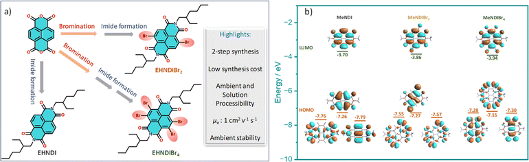 |
| | Scheme 1 (a) Structure and the speciality of the NDI derivatives under study and (b) computed frontier molecular orbital (FMO) distributions for three compounds with Me-side chains. Core Br-substituted NDI molecules indicating the contribution of the halogen groups' non-bonding orbitals to the HOMO in the last two cases. | |
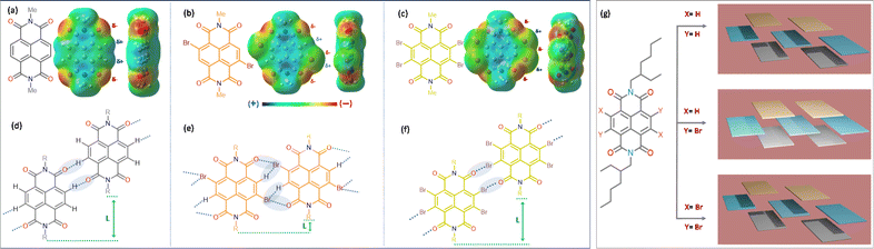 |
| | Fig. 1 Chemical structures and ESP maps of (a) MeNDI, (b) MeNDIBr2, and (c) MeNDIBr4 calculated at the B3LYP/6-31+G(d) level of DFT. Schematic lateral interactions, expected from (d) MeNDI, (e) MeNDIBr2, and (f) MeNDIBr4. (g) indicates the different brick-work stacks of molecules in three derivatives under study. Three different colors indicate three layers in each of them. | |
Optical and photophysical features
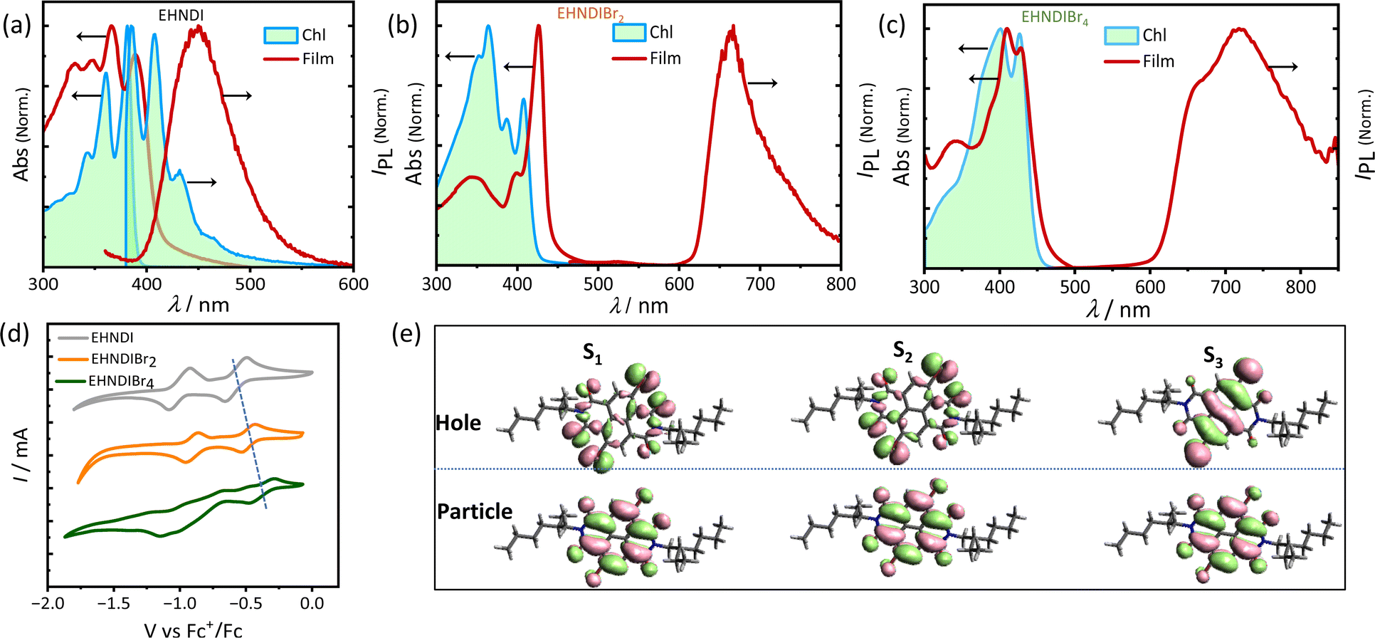
Optical properties of these NDI derivatives would offer valuable insights into their molecular assembly pathways. These properties were studied by UV-VIS absorption and PL spectroscopy using monomeric and aggregated films. Dilute chloroform solutions and thin film samples (Fig. 2a–c) were used. Introducing bromine atoms into the NDI core led to a redshift in the absorption band edge and a reduction in the optical bandgap (Eg). An additional transition, originating from Br-centered non-bonding orbitals, was predicted based on natural transition orbital (NTO) calculations (Fig. 2e). For EHNDIBr2 in CHCl3, we observed well-defined vibronic bands at 408 nm (0–0), 387 nm (0–1), and 364 nm (0–2), and a broader band at 349 nm. The thin film absorption spectra showed an 18 nm redshift in the 0–0 absorption band compared to the monomeric solution state, and the intensity ratio of this band (I0–0/I0–1) increased from 1.13 to 2.6, transitioning from the monomeric solution state to the film state. This shift suggested strong excitonic coupling in densely packed chromophores in film state samples.31 Corresponding vibronic bands in the film were at 426 nm (0–0), 398 nm (0–1), and 345 nm (0–2). For EHNDI films, the shift was less pronounced, only 9 nm (0–0) compared to the solution state (from 381 nm to 390 nm). EHNDIBr4 showed a 2 nm redshift, and its spectral profile in the film state was similar to the monomeric solution state, indicating minimal excitonic coupling. Photoluminescence (PL) spectra analysis showed that EHNDI exhibited structured emission in chloroform solution, while exhibiting a broad emission band centered near 460 nm, characteristic of NDI excimer emission. In contrast, the substituted derivatives EHNDIBr2 and EHNDIBr4 displayed non-luminescent behavior in solution, likely due to intersystem crossing and non-radiative triplets under ambient conditions, a phenomenon associated with the presence of heavy atoms like bromine, which can induce spin crossover in the excited state.32a,b Further, PL spectra of deaerated toluene solutions were also recorded, revealing intense emission bands at 665 nm and 715 nm for EHNDIBr2 and EHNDIBr4, respectively (Fig. S8†). This behavior underscores the complexity of the photophysical properties of NDI derivatives and their potential applications in electronic devices, where understanding and manipulating such properties are crucial for optimizing their performance. Overall, the optical studies demonstrate the significant impact of bromine substitution on the electronic structure and excitonic interactions and provide insights into the intricate interplay between the molecular structure, assembly, and photo-physics.
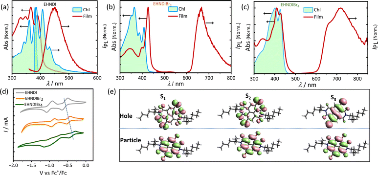 |
| | Fig. 2 (a) Solution and film state absorption spectra and emission spectra (a) EHNDI, (b) EHNDIBr2 and (c) EHNDIBr4. (d) Cyclic voltammograms (in reduction cycle) in CH2Cl2 solvent (vs. Fc/Fc+) of EHNDI, EHNDIBr2 and EHNDIBr4. (e) The NTO hole and particle distributions in the first, second and third excited states indicating the contribution of Br centric orbitals to the optical transition. | |
Electrochemical and thermal properties
Electrochemical redox properties of these derivatives were analysed using cyclic voltammetry (CV) in dichloromethane (CH2Cl2) at 25 °C, with gold (Au), silver/silver chloride (Ag/AgCl), and platinum (Pt) serving as the working, reference, and counter electrodes, respectively. The CV results (Fig. 2d) revealed two electron reversible reduction peaks, indicating the high electron affinity of these molecules. Consistent with expectations, bromination of the NDI core successively reduced the first onset reduction potential, indicating a deeper LUMO (Lowest Unoccupied Molecular Orbital) level upon introducing electronegative atoms into the core. The LUMO levels were calculated to be −3.82, −3.92, and −4.02 eV for EHNDI, EHNDIBr2, and EHNDIBr4, respectively, using ferrocene (Fc)/ferrocenium (Fc+) as an internal standard.33 These compounds' Ionization Potential (IP) values were estimated using Ultraviolet Photoelectron Spectroscopy (UPS). A progressive reduction in IP values was observed with adding bromine atoms, as shown in Fig. S10† and summarized in Table 1. The experimentally obtained parameters, including the HOMO (Highest Occupied Molecular Orbital), and values from CV and optical bandgap measurements, correlated well with the computed values. Further analysis of the materials' physical properties was conducted using Differential Scanning Calorimetry (DSC) and Thermal Gravimetric Analysis (TGA). All three compounds displayed high thermal stability (Fig. S9†), with decomposition onset temperatures exceeding 320 °C (Td). DSC analysis revealed the melting temperatures (Tm) of the molecules, with EHNDIBr2 exhibiting the highest melting temperature at 253 °C, compared to EHNDI (201 °C) and EHNDIBr4 (approximately 244 °C), despite variations in molecular mass. Intriguingly, the corresponding enthalpy changes (ΔHm) also showed notable differences. EHNDIBr2 had the highest melting enthalpy change at 53 kJ mol−1, which was 15% greater than that of EHNDIBr4 and 66% higher than that of EHNDI. These superior thermal parameters of EHNDIBr2 solids are attributed to the highest lattice energy among the derivatives, resulting from its unique structural features. The higher melting enthalpy indicates a more rigidly packed structure of EHNDIBr2 in the solid state, potentially contributing to lower effective lattice vibrations. This observation is consistent with the findings from single crystal structure analysis. Consequently, these structural characteristics of EHNDIBr2 contribute to its superior charge carrier transport properties, demonstrating its potential for efficient and stable performance in electronic devices.
Table 1 Summary of the molecular properties in solution and solid-states and the computed HOMO/LUMO levels for the NDI derivatives
|
|
Solution |
Solid-state |
Computed |
| LUMOa [eV] |
HOMOa,b [eV] |
E
g
[eV] |
IPc [eV] |
T
m
[°C] |
ΔHmd [kJ mol−1] |
T
d
[°C] |
HOMO [eV] |
LUMO [eV] |
|
Extracted from CV.
From UV absorption.
Estimated from UPS experiments.
Estimated from DSC experiments.
Measured from TGA experiments. ΔHm: enthalpy changed during melting. Eg: optical bandgap.
|
| EHNDI |
−3.8 |
−7.0 |
3.2 |
7.4 |
201 |
32 |
323 |
−7.3 |
−3.7 |
| EHNDIBr2 |
−3.9 |
−6.9 |
2.9 |
7.3 |
253 |
53 |
366 |
−7.3 |
−3.9 |
| EHNDIBr4 |
−4.0 |
−6.8 |
2.8 |
7.2 |
244 |
46 |
322 |
−7.2 |
−3.9 |
OFET device and charge transport characteristics
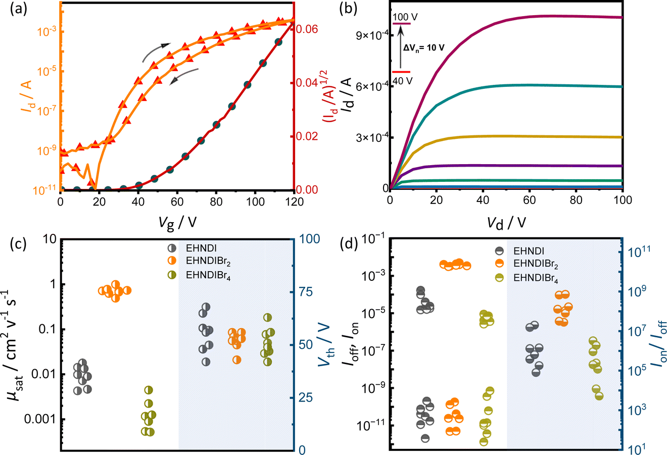
Organic field-effect transistors (OFETs) with bottom-gate top-contact (BG-TC) geometry were fabricated using solution-processed active layers. These layers were deposited by spin-coating 4–5 mg mL−1 chloroform (CHL) solutions of the molecules on n-octadecyltrichlorosilane (n-OTS) modified Si/SiO2 substrates.34 Optimal post-deposition thermal annealing conditions were determined for each derivative: 150 °C for EHNDIBr2, none for EHNDI, and 80 °C for EHNDIBr4. Gold (Au) source–drain (S–D) electrodes were then thermally evaporated onto the substrates. The EHNDIBr2 active layers exhibited impressive dopant-free electron mobility (μe) in the saturation regime, reaching up to 1.0 cm2 V−1 s−1, with an average mobility of 0.71 cm2 V−1 s−1 across 12 devices. This performance included a high on–off current ratio (Ion/Ioff > 108) and low hysteresis. In contrast, EHNDI and EHNDIBr4 showed significantly reduced carrier mobility, orders of magnitude lower than that of EHNDIBr2, with the best devices achieving μe values of 1.8 × 10⁻² cm2 V−1 s−1 and 4.5 × 10⁻³ cm2 V−1 s−1, respectively. Fig. 3 summarizes representative transfer and output characteristics of EHNDIBr2, and the summary of device performance is provided in Table 2. This considerable variation in carrier mobilities among the derivatives is primarily attributed to differences in π-overlap between neighboring molecules in their solid-state structures, as determined by film X-ray diffraction (GIXD and WAXD) measurements. EHNDIBr2's higher order of molecular assembly and higher degree of aggregation in the film state, compared to EHNDI and EHNDIBr4, result in superior charge transport. All devices exhibited high threshold voltage (Vth), regardless of the processing conditions, indicating high contact resistance due to an electron injection barrier at the semiconductor-S-D electrode interface. This suggests poor energy level alignment, potentially caused by mismatched work functions, interfacial and bulk traps, and interface morphology.35a,b Efforts are ongoing to minimize contact resistance and improve the threshold voltage.
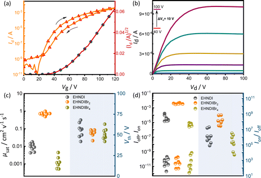 |
| | Fig. 3 OFET (a) transfer curve and (b) output curves for the EHNDIBr2 thin film. (c) μsat (left) and Vth (right) variations of EHNDI, EHNDIBr2, and EHNDIBr4 devices. (d) Ion (top left), Ioff (bottom left), and Ion/Ioff (right) variations of EHNDI, EHNDIBr2, and EHNDIBr4 devices. | |
Table 2 Summary of the performances of OFET devices, prepared under optimized conditions and their ambient storage stability (75% atmospheric humidity)a
|
|
Annealing T/°C |
μ
avge (cm2 V−1 s−1) |
μ
maxe (cm2 V−1 s−1) |
V
th (V) |
I
ON/IOFF |
μ
avge retention (%) |
|
Mobility retention (in %) after 85 h.
|
| EHNDI |
NA |
0.9 × 10⁻² |
1.8 × 10⁻² |
56 |
>107 |
16 |
| EHNDIBr2 |
150 |
0.71 |
1.0 |
52 |
>108 |
66 |
| EHNDIBr4 |
80 |
1.6 × 10⁻³ |
4.5 × 10⁻³ |
49 |
>106 |
67 |
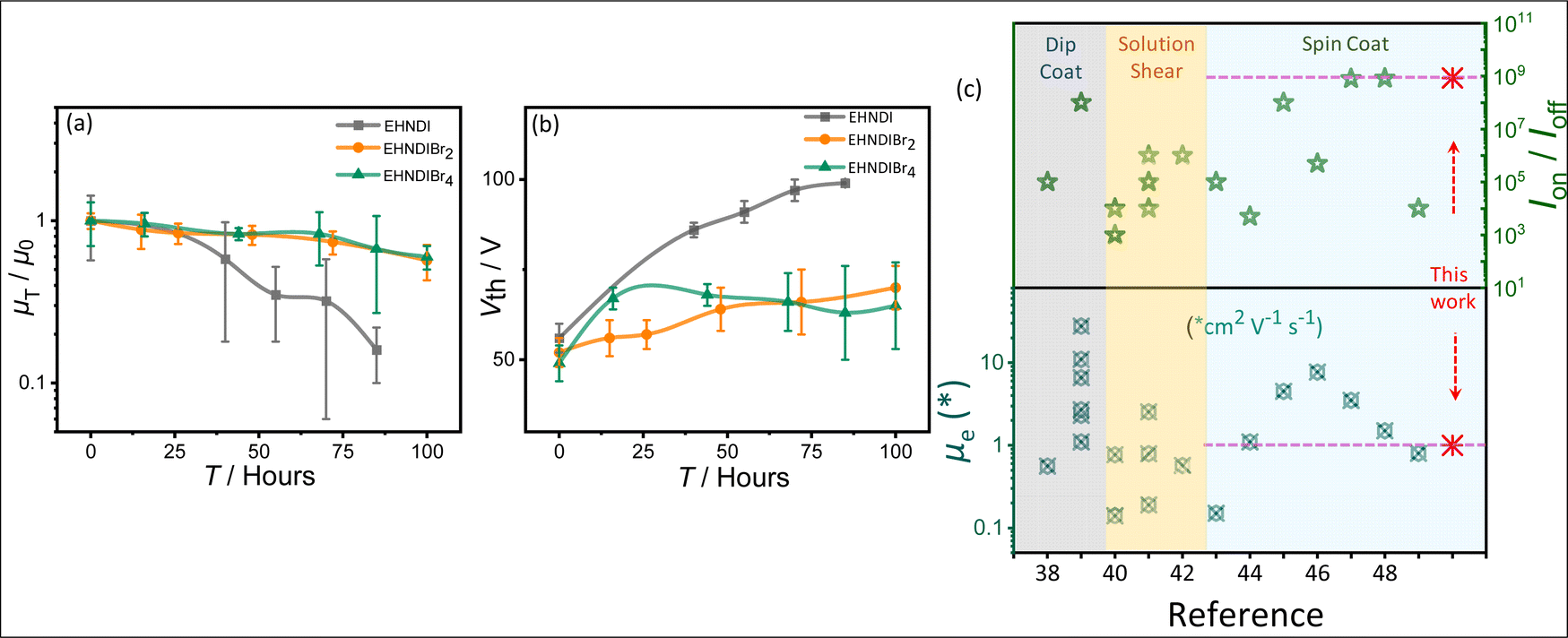
A reliability factor (r) was introduced to ensure accuracy in carrier mobility extraction, accounting for high Vth in devices.36 The r factors were found to be 30 ± 2% for all devices. EHNDIBr2's high carrier mobility is credited to its low π-stacking distance, significant π-overlap, low in-plane molecular slip, and well-organized packing in the film state, as observed in single crystal structural analysis and GIXRD measurements. It is known that in the brickwork stack of planar aromatic diimides, the long-axis displacement between the neighboring pair in a π-stack affects the charge transfer integral more intensely than the short-axis displacement.30a The same hypothesis can be extended to the above example of EHNDIBr2. Ambient stability was also assessed for these OFET devices, considering that a deep LUMO (<−4.0 eV) is crucial for operational stability.37 Electrical characterization over 100 hours under ambient conditions (75% humidity) showed that the average charge carrier mobility after 85 hours remained around 16%, 66%, and 67% for EHNDI, EHNDIBr2, and EHNDIBr4, respectively (Fig. 4a). EHNDIBr2 and EHNDIBr4's better ambient stability is attributed to the hydrophobic effect of Br atoms in the NDI core and their low-lying LUMO levels, which likely hinder moisture diffusion and interfacial charge trapping.
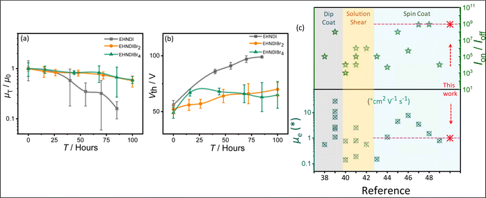 |
| | Fig. 4 Ambient stability measurement: (a) average saturation mobility change and (b) the threshold voltage changes (ΔVth) with time of the OFET devices with exposure to the ambient atmosphere. (c) Summarized literature reports on the best device performances.38–49 PVD processed and single crystal devices excluded. | |
The EHNDI-based devices degraded under ambient exposure, indicating faster air/moisture diffusion and reactivity as EHNDI has higher LUMO values and no hydrophobic groups in the core. The average threshold voltage shifts (ΔVth) were 43 V, 15 V and 13 V for EHNDI, EHNDIBr2 and EHNDIBr4, respectively (Fig. 4b). This possibly indicates the incorporation of charge-trapping states at the dielectric/active layer interface from the atmosphere and the damage of the metal-OSC interfaces by the air. The damage is highest in the case of EHNDI and lowest for EHNDIBr4.
Single crystal structure analysis
The study of solid-state molecular interactions and packing in EHNDI, EHNDIBr2 and EHNDIBr4 was conducted using single-crystal X-ray diffraction experiments (CCDC numbers: 2346855, 2323962, 2323963).† All three compounds crystallized in the triclinic space group P![[1 with combining macron]](https://www.rsc.org/images/entities/char_0031_0304.gif) . The molecular structure of EHNDI demonstrates planar conformations of the NDI core. Intermolecular interactions primarily involve C–H⋯O attractive forces, with a distance measuring 2.45 Å (Fig. 5a and S14†). The interplanar π–π stacking distance is around 3.3 Å. In the molecular structure of EHNDIBr2, the NDI core also exhibits planar conformations. The intermolecular interactions are characterized mainly by two types of attractive forces: C–H⋯Br (with a distance of 2.94 Å) and C–Br⋯O (3.14 Å) interactions (Fig. 5b and S14†). These distances are shorter than the summation of their van der Waals radii (H⋯Br = 3.05 Å and Br⋯O = 3.37 Å),50 indicating efficient intermolecular interactions, resulting in the low longitudinal misalignment (L) of two lateral neighbors. Additionally, a noticeable intermolecular steric hindrance and structural locking among the adjacent molecules were evident, which also imparted additional stability to the molecular stack. Precisely speaking, the hindrance was among the branched ethyl unit of the side chains between the neighboring molecules and an ethyl–hexyl unit of a molecule, and the core substituted Br atom of the same (Fig. 5d). These steric and intermolecular interactions helped to lock the dimers, minimizing longitudinal slip along the long molecular axis. The low longitudinal misalignment (L) between lateral neighbors enhances π-stacking, while steric hindrance and structural locking among adjacent molecules provide additional stability to the molecular stack. This unique arrangement results in effective π-overlap between adjacent stacks, leading to asymmetric π-stacks with low displacement values of 0.79 and 0.82 Å. The 2-D brickwork packing in EHNDIBr2, characterized by face-to-face stacking and molecular overlaps, contributes to its high charge carrier mobility. In contrast, EHNDIBr4 exhibits major lateral interactions such as C–O⋯Br (around 2.92 Å) and C–H⋯Br (2.91 Å) (alkyl chain H) (Fig. 5c and S14†). However, the absence of (i) core-bromines in EHNDI and (ii) core-hydrogens in EHNDIBr4 results in different interaction possibilities compared to EHNDIBr2, leading to a relatively large longitudinal displacement in the former pair. Despite a short inter-planar distance (3.3–3.4 Å) (Fig. 5f and g), EHNDI and EHNDIBr4 show a mix of good and minimal π-overlap in their asymmetric π-stacks, which affects their charge transport properties. The presence of one stack with low L (approximately 0.96 Å and 0.78 Å for EHNDI and EHNDIBr4 respectively) indicates good π-overlap, while another stack with high L (approximately 5.2 Å and 6.9 Å for EHNDI and EHNDIBr4 respectively) shows minimal overlap, resulting in weaker 2-D charge transport features for both EHNDI and EHNDIBr4. The increased displacement observed in EHNDIBr4 compared to EHNDI suggests even poorer charge transport in EHNDIBr4, a conclusion supported by the device results. These findings demonstrate how the molecular structure and intermolecular interactions within the solid-state significantly influence the electronic properties of these materials, particularly in relation to their charge transport capabilities. The distinct molecular arrangements and packing in EHNDI, EHNDIBr2 and EHNDIBr4 lead to notably different electronic performances, with EHNDIBr2 showing superior charge carrier mobility due to its more effective π-stacking and molecular interactions.
. The molecular structure of EHNDI demonstrates planar conformations of the NDI core. Intermolecular interactions primarily involve C–H⋯O attractive forces, with a distance measuring 2.45 Å (Fig. 5a and S14†). The interplanar π–π stacking distance is around 3.3 Å. In the molecular structure of EHNDIBr2, the NDI core also exhibits planar conformations. The intermolecular interactions are characterized mainly by two types of attractive forces: C–H⋯Br (with a distance of 2.94 Å) and C–Br⋯O (3.14 Å) interactions (Fig. 5b and S14†). These distances are shorter than the summation of their van der Waals radii (H⋯Br = 3.05 Å and Br⋯O = 3.37 Å),50 indicating efficient intermolecular interactions, resulting in the low longitudinal misalignment (L) of two lateral neighbors. Additionally, a noticeable intermolecular steric hindrance and structural locking among the adjacent molecules were evident, which also imparted additional stability to the molecular stack. Precisely speaking, the hindrance was among the branched ethyl unit of the side chains between the neighboring molecules and an ethyl–hexyl unit of a molecule, and the core substituted Br atom of the same (Fig. 5d). These steric and intermolecular interactions helped to lock the dimers, minimizing longitudinal slip along the long molecular axis. The low longitudinal misalignment (L) between lateral neighbors enhances π-stacking, while steric hindrance and structural locking among adjacent molecules provide additional stability to the molecular stack. This unique arrangement results in effective π-overlap between adjacent stacks, leading to asymmetric π-stacks with low displacement values of 0.79 and 0.82 Å. The 2-D brickwork packing in EHNDIBr2, characterized by face-to-face stacking and molecular overlaps, contributes to its high charge carrier mobility. In contrast, EHNDIBr4 exhibits major lateral interactions such as C–O⋯Br (around 2.92 Å) and C–H⋯Br (2.91 Å) (alkyl chain H) (Fig. 5c and S14†). However, the absence of (i) core-bromines in EHNDI and (ii) core-hydrogens in EHNDIBr4 results in different interaction possibilities compared to EHNDIBr2, leading to a relatively large longitudinal displacement in the former pair. Despite a short inter-planar distance (3.3–3.4 Å) (Fig. 5f and g), EHNDI and EHNDIBr4 show a mix of good and minimal π-overlap in their asymmetric π-stacks, which affects their charge transport properties. The presence of one stack with low L (approximately 0.96 Å and 0.78 Å for EHNDI and EHNDIBr4 respectively) indicates good π-overlap, while another stack with high L (approximately 5.2 Å and 6.9 Å for EHNDI and EHNDIBr4 respectively) shows minimal overlap, resulting in weaker 2-D charge transport features for both EHNDI and EHNDIBr4. The increased displacement observed in EHNDIBr4 compared to EHNDI suggests even poorer charge transport in EHNDIBr4, a conclusion supported by the device results. These findings demonstrate how the molecular structure and intermolecular interactions within the solid-state significantly influence the electronic properties of these materials, particularly in relation to their charge transport capabilities. The distinct molecular arrangements and packing in EHNDI, EHNDIBr2 and EHNDIBr4 lead to notably different electronic performances, with EHNDIBr2 showing superior charge carrier mobility due to its more effective π-stacking and molecular interactions.
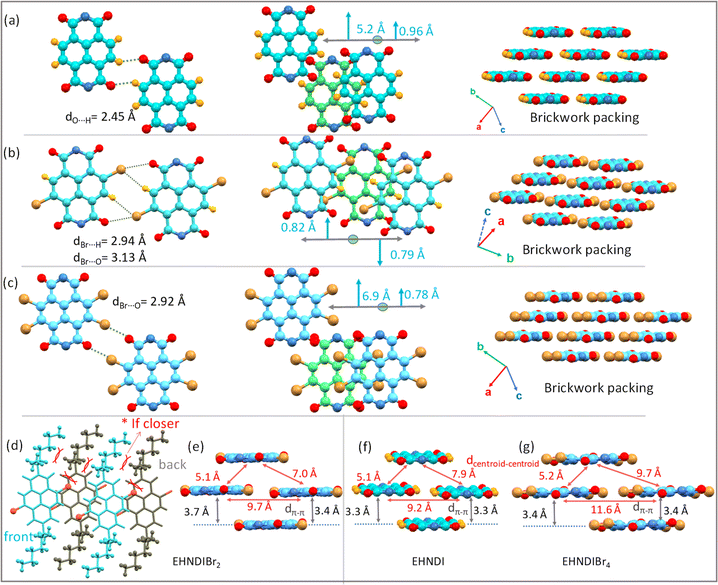 |
| | Fig. 5 Single crystal molecular packing and 2-D brickwork packing motifs for EHNDI, EHNDIBr2 and EHNDIBr4: lateral intermolecular interactions, short contacts and packing motifs for (a) EHNDI, (b) EHNDIBr2 and for (c) EHNDIBr4. (d) Representation of the steric locking in EHNDIBr2. Nearest neighbor intermolecular distances in the adjacent stacks for (e) EHNDIBr2, (f) EHNDI and (g) EHNDIBr4. | |
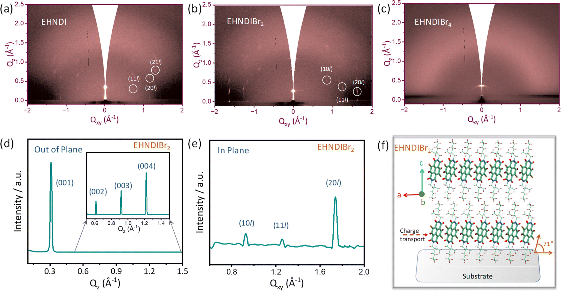
Film state WXRD and GIXRD
Out-of-plane wide-angle XRD measurements (WXRD) were conducted on OTS-modified Si/SiO2 substrates (Fig. S15h†). Considering the molecular dimensions, plausible molecular stacking on substrates was simulated following known reports of NDI-derived materials. At first glance, EHNDIBr2 films exhibited more crystalline domains than the other two, considering the higher order of diffraction from its sample surface. Considering the d-values of the first-order signal and the molecular dimension (end-to-end distance of ∼21.5 Å as obtained from their single crystal structures), along with the absence of reflection due to π–π ordering (around 2θ = 25°–30°), we confirmed that vertical molecular alignment on the substrate surface (ordering along 001) is prevailing. Higher-order reflections indicating extended periodicity along the vertical direction confirmed well-organized lamellar supramolecular structures of EHNDIBr2 on the substrate surface. The position of the first-order signal for the latter pair was at 2θ = 5.8–6.1°, whereas it was 4.28° for EHNDIBr2. This difference in the first-order reflection position for the former pair is attributed primarily to the inclined molecular long axis on the surface, as indicated in Fig. S15.† Comparing the molecular length and the first-order reflections, a relative inclination of the molecular long axis is predicted to be ∼73° for EHNDIBr2 and ∼43°–45° for the other two derivatives. Further, on comparing the simulated powder XRD patterns from the SCXRD data and the experimentally obtained film state WAXRD of EHNDIBr2, we confirmed that the planes (00N) were positioned parallel to the substrate with the unit cell axes a and b on the parallel plane. Subsequently, EHNDIBr2 molecules are positioned on the substrate surface with the π–π stacking direction parallel to the substrate surface, which helps to achieve excellent 2D charge transport.
To understand the in-plane periodicity in the bulk films deposited on the substrates, and alterations of the diverse packing patterns, including molecular orientations, GIXRD measurements were conducted on oxide substrates. EHNDIBr2 films exhibited in-plane and out-of-plane (qz and qxy) ordering indicative of strong signals, as shown in (Fig. 6b and S15†). In contrast, weak in-plane diffractions were observed in the case of the EHNDI-film, indicating weak long-range in-plane ordering and no out-of-plane signals were observed, indicating extremely weak lamellar ordering along the vertical direction. For EHNDIBr4 films, neither in-pane nor out-of-plane signals were evident, which confirms a highly amorphous character (Fig. 6c and S15†) as indicated in the WXRD experiment (vide supra). Additionally, the (00l) ordered patterns along qz were visibly spotted for EHNDIBr2 films (Fig. 6d), which appeared as higher ordered (001) to (004) peaks, inferring a controlled edge-on molecular orientation (Fig. 6f). The conjugated backbones are aligned perpendicular to the substrate, having strong intermolecular π-stacking interactions, which is the most favorable condition for lateral charge transport in devices such as OFETs. The qzd-spacing (from (001) peak) of 20.3 Å again confirmed that the molecular long axis is positioned at nearly 71° tilt angle (as the molecular length of 21.5 Å). The qxyd-spacing value calculated from the (20l) peak of the in-plane profile (Fig. 6e) is 3.6 Å, signifying π–π stacking distances, which endorse the value obtained from a single crystal structure. The 2-D diffraction profile of EHNDI indicated less ordering in their film states with a minimum d-spacing of 4.1 Å in qxy (Fig. S15†). On the other hand, EHNDIBr4 displayed only (001) diffraction spots lacking higher-order signals, indicating a lack of periodic ordering in both the lateral (xy) and z directions. To summarize, EHNDIBr2 is expected to have the most favorable molecular orientation on surfaces to facilitate the charge carrier transport, while EHNDIBr4 has the least.
 |
| | Fig. 6 (a–c) 2-D GIXRD diffraction profile of the optimized samples, (d) and (e) 1-D line cut profile of the EHNDIBr2 films: (e) in-plane and (d) out-of-plane indicating periodic reflections of 001 planes. (f) Plausible molecular ordering on the surface. | |
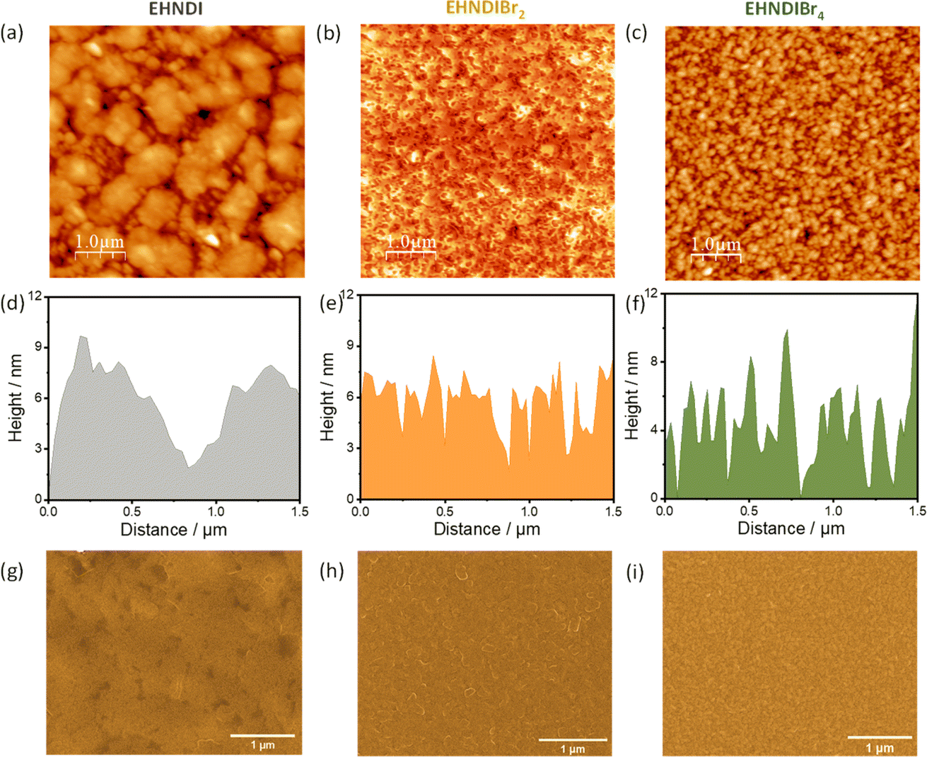
AFM and SEM analysis
To understand the effect of film morphologies on charge transport, atomic force microscopy (AFM) and scanning electron microscopy (SEM) experiments were carried out on the films, keeping the device deposition condition fixed. Fig. 7 shows AFM and SEM images for all three molecules. Fig. 7a shows the large micron-size grains in the film state of EHNDI with a few visible grain boundaries, whereas many small grains (∼80–100 nm) containing large numbers of boundaries were observed in the case of EHNDIBr4 (Fig. 7c). Significant grain boundaries create high resistance for charge transport through the bulk, which is observed in the lowest μe value of EHNDIBr4.42,51 Both the compounds contain relatively higher roughness (root-mean-square (RMS) roughness, EHNDI: 4.8 nm and EHNDIBr4: 3.18 nm) than EHNDIBr2 (RMS: 2.66 nm). EHNDIBr2, consisting of highly crystalline domains in the film state (Fig. 7b), shows a relatively smooth surface with very few grain boundaries, which is favourable for excellent charge transport.
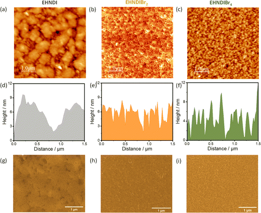 |
| | Fig. 7 AFM topography images, AFM height profiles and SEM images (a), (d), and (g) for EHNDI, (b), (e), and (h) for EHNDIBr2 and (c), (f), and (i) for EHNDIBr4 respectively. | |
Conclusion
The structural requirements of efficient n-type organic semiconductors and their device characteristics are summarized here. A simple and known skeletal unit (NDI) was considered for the case study, and the core unit was derivatized by Br atom substitution to yield three derivatives for studies. The most efficient candidate (EHNDIBr2) in terms of processibility, superior carrier mobility and ambient stability was subjected to critical analysis. Brickwork supramolecular stacks were confirmed by single crystal XRD studies. Interestingly, rigid in-plane molecular ordering originated from steric locking mode, and multiple favourable non-covalent interactions were holding the molecular hoping centres, minimizing the longitudinal dimeric slip, and possibly lowering the thermal oscillations in the bulk lattice. The structural and stability of the samples were confirmed by a detailed thermal analysis. Our multi-faceted approach on picking up the right molecular unit is expected to trigger a new design strategy. We expect that our report on n-type molecular semiconductors substantially advances organic electronics.
Data availability
The data (experimental procedures, characterization data and DFT calculations) that support this article is available within the article and its ESI.†
Author contributions
IG, SC, and JJP conducted the synthesis and characterization of all compounds. IG has performed electrical characterizations, single crystal packing analysis, microscopy, 2D GIXRD, optical and electrochemical experiments and analysis, as well as DFT-ESP calculations. MM performed the NTO calculation. ABD provided guidance for 2D GIXRD experiments and analysis. RV conceptualized and supervised the project.
Conflicts of interest
The authors declare no competing financial interests.
Acknowledgements
IG and JJ thank UGC, and SC and MM thank CSIR-India for their fellowships. This work was supported by IGSTC 2+2 LABELONIK and CRG/2021/006054. We acknowledge DESY (Hamburg, Germany), a member of the Helmholtz Association HGF, for the provision of experimental facilities. Parts of this research were carried out at the P08 beamline, PETRA III, DESY, Germany. Beamtime was allocated for proposal(s) (project no. I-20221013, I-20211469). We acknowledge financial support by the Department of Science & Technology, Government of India (DST), provided within the framework of the India@Desy collaboration. We also acknowledge Dr Surojit Bhunia and Mr Kaustav Das for helping in solving crystal structures. The authors thank Dr Rahul Banerjee for the fruitful discussions.
References
- J. Chen, W. Zhang, L. Wang and G. Yu, Adv. Mater., 2023, 35, 2210772 CrossRef CAS PubMed.
- H. Katz, A. Lovinger, J. Johnson, C. Kloc, T. Siegrist, W. Li, Y. Lin and A. Dodabalapur, Nature, 2000, 404, 478–481 CrossRef CAS PubMed.
- D. Shukla, S. F. Nelson, D. C. Freeman, M. Rajeswaran, W. G. Ahearn, D. M. Meyer and J. T. Carey, Chem. Mater., 2008, 20, 7486–7491 CrossRef CAS.
- D. Bialas, E. Kirchner, M. I. S. Röhr and F. Würthner, J. Am. Chem. Soc., 2021, 143, 4500–4518 CrossRef CAS PubMed.
- M. M. Ling, P. Erk, M. Gomez, M. Koenemann, J. Locklin and Z. Bao, Adv. Mater., 2007, 19, 1123–1127 CrossRef CAS.
- X. Cui, C. Xiao, T. Winands, T. Koch, Y. Li, L. Zhang, N. L. Doltsinis and Z. Wang, J. Am. Chem. Soc., 2018, 140, 12175–12180 CrossRef CAS PubMed.
- A. Velusamy, C. H. Yu, S. N. Afraj, C. C. Lin, W. T. Lo, C. J. Yeh, Y. W. Wu, H. C. Hsieh, J. Chen, G. H. Lee, S. H. Tung, C. L. Liu, M. C. Chen and A. Facchetti, Adv. Sci., 2021, 8, 2002930 CrossRef CAS PubMed.
- S. Fratini, M. Nikolka, A. Salleo, G. Schweicher and H. Sirringhaus, Nat. Mater., 2020, 19, 491–502 CrossRef CAS PubMed.
- J. E. Anthony, J. S. Brooks, D. L. Eaton and S. R. Parkin, J. Am. Chem. Soc., 2001, 123, 9482–9483 CrossRef CAS PubMed.
- M. Mas-Torrent and C. Rovira, Chem. Rev., 2011, 111, 4833–4856 CrossRef CAS PubMed.
- K. J. Kalita, I. Giri and R. K. Vijayaraghavan, RSC Adv., 2021, 11, 33703–33713 RSC.
- R. Kroon, D. A. Mengistie, D. Kiefer, J. Hynynen, J. D. Ryan, L. Yu and C. Müller, Chem. Soc. Rev., 2016, 45, 6147–6164 RSC.
-
(a) C. Luo, A. K. K. Kyaw, L. A. Perez, S. Patel, M. Wang, B. Grimm, G. C. Bazan, E. J. Kramer and A. J. Heeger, Nano Lett., 2014, 14, 2764–2771 CrossRef CAS PubMed;
(b) K. Liu, B. Ouyang, X. Guo, Y. Guo and Y. Liu, npj Flexible Electron., 2022, 6, 1 CrossRef CAS;
(c) T. Okamoto, S. Kumagai, E. Fukuzaki, H. Ishii, G. Watanabe, N. Niitsu, T. Annaka, M. Yamagishi, Y. Tani, H. Sugiura, T. Watanabe, S. Watanabe and J. Takeya, Sci. Adv., 2020, 6, eaaz0632 CrossRef CAS PubMed.
- P. A. Banks, G. D'Avino, G. Schweicher, J. Armstrong, C. Ruzié, J. W. Chung, J. Park, C. Sawabe, T. Okamoto, J. Takeya, H. Sirringhaus and M. T. Ruggiero, Adv. Funct. Mater., 2023, 33, 2303701 CrossRef CAS.
- T. Hodsden, K. J. Thorley, J. Panidi, A. Basu, A. V. Marsh, H. Dai, A. J. P. White, C. Wang, W. Mitchell, F. Glöcklhofer, T. D. Anthopoulos and M. Heeney, Adv. Funct. Mater., 2020, 30, 2000325 CrossRef CAS.
- M. A. Stoeckel, Y. Olivier, M. Gobbi, D. Dudenko, V. Lemaur, M. Zbiri, A. A. Y. Guilbert, G. D'Avino, F. Liscio, A. Migliori, L. Ortolani, N. Demitri, X. Jin, Y. G. Jeong, A. Liscio, M. V. Nardi, L. Pasquali, L. Razzari, D. Beljonne, P. Samorì and E. Orgiu, Adv. Mater., 2021, 33, 2007870 CrossRef CAS PubMed.
- C. P. Yu, S. Kumagai, T. Kushida, M. Mitani, C. Mitsui, H. Ishii, J. Takeya and T. Okamoto, J. Am. Chem. Soc., 2022, 144, 11159–11167 CrossRef CAS PubMed.
- J. H. Dou, Z. A. Yu, J. Zhang, Y. Q. Zheng, Z. F. Yao, Z. Tu, X. Wang, S. Huang, C. Liu, J. Sun, Y. Yi, X. Cao, Y. Gao, J. Y. Wang and J. Pei, J. Am. Chem. Soc., 2019, 141, 6561–6568 CrossRef CAS PubMed.
- J. E. Anthony, Chem. Rev., 2006, 106, 5028–5048 CrossRef CAS PubMed.
- T. Yamamoto and K. Takimiya, J. Am. Chem. Soc., 2007, 129, 2224–2225 CrossRef CAS PubMed.
- H. Sirringhaus, Adv. Mater., 2014, 26, 1319–1335 CrossRef CAS PubMed.
- H. Iino, T. Usui and J. I. Hanna, Nat. Commun., 2015, 6, 6828 CrossRef CAS PubMed.
- B. A. Jones, M. J. Ahrens, M. H. Yoon, A. Facchetti, T. J. Marks and M. R. Wasielewski, Angew. Chem., Int. Ed., 2004, 43, 6363–6366 CrossRef CAS PubMed.
- T. He, M. Stolte and F. Würthner, Adv. Mater., 2013, 25, 6951–6955 CrossRef CAS PubMed.
- J. M. Mativetsky, E. Orgiu, I. Lieberwirth, W. Pisula and P. Samorì, Adv. Mater., 2014, 26, 430–435 CrossRef CAS PubMed.
- K. Shi, W. Zhang, D. Gao, S. Zhang, Z. Lin, Y. Zou, L. Wang and G. Yu, Adv. Mater., 2018, 30, 1705286 CrossRef PubMed.
- L. T. Ming, H. O. Joon, A. D. Reichardt and Z. Bao, J. Am. Chem. Soc., 2009, 131, 3733–3740 CrossRef PubMed.
- S. Kumagai, H. Ishii, G. Watanabe, T. Annaka, E. Fukuzaki, Y. Tani, H. Sugiura, T. Watanabe, T. Kurosawa, J. Takeya and T. Okamoto, Chem. Mater., 2020, 32, 9115–9125 CrossRef CAS.
- D. Gunturkun, R. Isci, S. Faraji, B. Sütay, L. A. Majewski and T. Ozturk, J. Mater. Chem. C, 2023, 11, 13129–13141 RSC.
-
(a) M. C. R. Delgado, E. G. Kim, D. A. S. Filho and J. L. Bredas, J. Am. Chem. Soc., 2010, 132, 3375–3387 CrossRef PubMed;
(b) S. Kumagai, H. Ishii, G. Watanabe, C. P. Yu, S. Watanabe, J. Takeya and T. Okamoto, Acc. Chem. Res., 2022, 55, 660–672 CrossRef CAS PubMed.
- N. J. Hestand and F. C. Spano, Chem. Rev., 2018, 118, 7069–7163 CrossRef CAS PubMed.
-
(a) S. Guo, W. Wu, H. Guo and J. Zhao, J. Org. Chem., 2012, 77, 3933–3943 CrossRef CAS PubMed;
(b) M. Mondal, I. Giri, R. Patra, M. Das and R. K. Vijayaraghavan, Chem. Mater., 2023, 35, 6527–6537 CrossRef CAS.
- B. K. Barman, N. G. Ghosh, I. Giri, C. Kumar, S. S. Zade and R. K. Vijayaraghavan, Nanoscale, 2021, 13, 6759–6763 RSC.
- I. Giri, S. Biswas, S. Chhetri, A. Choudhuri, I. Mondal, S. P Senanayak, P. Krishnan Iyer, D. Chaudhuri and R. K. Vijayaraghavan, RSC Adv., 2024, 14, 7915–7923 RSC.
-
(a) M. Waldrip, O. D. Jurchescu, D. J. Gundlach and E. G. Bittle, Adv. Funct. Mater., 2020, 30, 1904576 CrossRef CAS;
(b) G. Choi, S. Oh, J. Seo and H. S. Lee, Adv. Funct. Mater., 2020, 30, 2002979 CrossRef CAS.
- H. H. Choi, K. Cho, C. D. Frisbie, H. Sirringhaus and V. Podzorov, Nat. Mater., 2018, 17, 2–7 CrossRef CAS PubMed.
- J. Dhar, U. Salzner and S. Patil, J. Mater. Chem. C, 2017, 5, 7404–7430 RSC.
- H. Reiss, L. Ji, J. Han, S. Koser, O. Tverskoy, J. Freudenberg, F. Hinkel, M. Moos, A. Friedrich, I. Krummenacher, C. Lambert, H. Braunschweig, A. Dreuw, T. B. Marder and U. H. F. Bunz, Angew. Chem., Int. Ed., 2018, 57, 9543–9547 CrossRef CAS PubMed.
- M. Chu, J. X. Fan, S. Yang, D. Liu, C. F. Ng, H. Dong, A. M. Ren and Q. Miao, Adv. Mater., 2018, 30, 1803467 CrossRef PubMed.
- S. Vegiraju, A. A. A. Torimtubun, P. S. Lin, H. C. Tsai, W. C. Lien, C. S. Chen, G. Y. He, C. Y. Lin, D. Zheng, Y. F. Huang, Y. C. Wu, S. L. Yau, G. H. Lee, S. H. Tung, C. L. Wang, C. L. Liu, M. C. Chen and A. Facchetti, ACS Appl. Mater. Interfaces, 2020, 12, 25081–25091 CrossRef CAS PubMed.
- A. Velusamy, C. H. Yu, S. N. Afraj, C. C. Lin, W. Y. Lo, C. J. Yeh, Y. W. Wu, H. C. Hsieh, J. Chen, G. H. Lee, S. H. Tung, C. L. Liu, M. C. Chen and A. Facchetti, Adv. Sci., 2021, 8, 2002930 CrossRef CAS PubMed.
- W. Y. Lee, J. H. Oh, S. L. Suraru, W. C. Chen, F. Würthner and Z. Bao, Adv. Funct. Mater., 2011, 21, 4173–4181 CrossRef CAS.
- P. Kafourou, B. Park, J. Luke, L. Tan, J. Panidi, F. Glöcklhofer, J. Kim, T. D. Anthopoulos, J. S. Kim, K. Lee, S. Kwon and M. Heeney, Angew. Chem., Int. Ed., 2021, 60, 5970–5977 CrossRef CAS PubMed.
- P. Kafourou, M. I. Nugraha, A. Nikitaras, L. Tan, Y. Firdaus, F. Aniés, F. Eisner, B. Ding, J. Wenzel, M. Holicky, L. Tsetseris, T. D. Anthopoulos and M. Heeney, ACS Mater. Lett., 2022, 4, 165–174 CrossRef CAS.
- C. Zhang, D. Yuan, H. Wu, E. Gann, L. Thomsen, C. R. McNeill, C. Di, X. Zhu and D. Zhu, J. Mater. Chem. C, 2017, 5, 1935–1943 RSC.
- Y. Xiong, J. Tao, R. Wang, X. Qiao, X. Yang, D. Wang, H. Wu and H. Li, Adv. Mater., 2016, 28, 5949–5953 CrossRef CAS PubMed.
- F. Zhang, Y. Hu, T. Schuettfort, C. A. Di, X. Gao, C. R. McNeill, L. Thomsen, S. C. B. Mannsfeld, W. Yuan, H. Sirringhaus and D. Zhu, J. Am. Chem. Soc., 2013, 135, 2338–2349 CrossRef CAS PubMed.
- G. Liu, C. Xiao, F. Negri, Y. Li and Z. Wang, Angew. Chem., Int. Ed., 2020, 59, 2008–2012 CrossRef CAS PubMed.
- G. Lin, Y. Qin, J. Zhang, Y. S. Guan, H. Xu, W. Xu and D. Zhu, J. Mater. Chem. C, 2016, 4, 4470–4477 RSC.
- A. Bondi, J. Phys. Chem., 1964, 68, 441–451 CrossRef CAS.
- H. H. Choi, A. F. Paterson, M. A. Fusella, J. Panidi, O. Solomeshch, N. Tessler, M. Heeney, K. Cho, T. D. Anthopoulos, B. P. Rand and V. Podzorov, Adv. Funct. Mater., 2020, 30, 1903617 CrossRef CAS.
|
| This journal is © The Royal Society of Chemistry 2024 |
Click here to see how this site uses Cookies. View our privacy policy here. 
 Open Access Article
 This Open Access Article is licensed under a Creative Commons Attribution-Non Commercial 3.0 Unported Licence
 *a
*a