
 Open Access Article
 This Open Access Article is licensed under a
 Creative Commons Attribution 3.0 Unported Licence
Mild chemistry synthesis of ultrathin Bi2O2S nanosheets exhibiting 2D-ferroelectricity at room temperature†
Riddhimoy
Pathak
a,
Prabir
Dutta
a,
Kapildeb
Dolui
b,
Aastha
Vasdev
c,
Adrija
Ghosh
a,
Raj Sekhar
Roy
d,
Ujjal K.
Gautam
d,
Tapas Kumar
Maji
 ae,
Goutam
Sheet
c and
Kanishka
Biswas
*a
ae,
Goutam
Sheet
c and
Kanishka
Biswas
*a
aNew Chemistry Unit, International Centre for Materials Science, School of Advanced Materials, Jawaharlal Nehru Centre for Advanced Scientific Research (JNCASR), Jakkur P.O., Bangalore 560064, India. E-mail: kanishka@jncasr.ac.in
bDepartment of Materials Science & Metallurgy, University of Cambridge, 27 Charles Babbage Road, Cambridge CB3 0FS, UK
cDepartment of Physical Sciences, Indian Institute of Science Education and Research Mohali, Sector 81, S. A. S. Nagar, Manauli, P.O. Box 140306, India
dDepartment of Chemical Sciences, Indian Institute of Science Education and Research Mohali, Sector 81, S. A. S. Nagar, Manauli, P.O. Box 140306, India
eChemistry and Physics of Materials Unit, Jawaharlal Nehru Centre for Advanced Scientific Research (JNCASR), Jakkur P.O., Bangalore 560064, India
First published on 9th April 2024
Abstract
Modern technology demands miniaturization of electronic components to build small, light, and portable devices. Hence, discovery and synthesis of new non-toxic, low cost, ultra-thin ferroelectric materials having potential applications in various electronic and optoelectronic devices are of paramount importance. However, achieving room-temperature ferroelectricity in two dimensional (2D) ultra-thin systems remains a major challenge as conventional three-dimensional ferroelectric materials lose their ferroelectricity when the thickness is brought down below a critical value owing to the depolarization field. Herein, we report room-temperature ferroelectricity in ultra-thin single-crystalline 2D nanosheets of Bi2O2S synthesized by a simple, rapid, and scalable solution-based soft chemistry method. The ferroelectric ground state of Bi2O2S nanosheets is confirmed by temperature-dependent dielectric measurements as well as piezoelectric force microscopy and spectroscopy. High resolution transmission electron microscopy analysis and density functional theory-based calculations suggest that the ferroelectricity in Bi2O2S nanosheets arises due to the local distortion of Bi2O2 layers, which destroys the local inversion symmetry of Bi2O2S.
Introduction
Since the discovery of graphene in 2004,1 scientists are driven to find novel atomically thin two dimensional (2D) layered materials showing striking optical,2–5 electrical,6–8 thermoelectric,9,10 and mechanical11 properties. The intriguing aspect of these properties measured in 2D materials is that they differ significantly from their bulk counterpart. However, experimental realization of room-temperature ferroelectricity in ultra-thin 2D materials is extremely challenging but it is of paramount importance for electronics and optoelectronics like random access memory, logic devices,12–14etc.Conventional three-dimensional ferroelectric materials like BaTiO3 and PbTiO3 lose their ferroelectricity when the thickness is brought down below a critical value owing to the depolarization field.15–17 Nevertheless, there are several theoretical predictions of ferroelectricity in 2D materials such as monolayers of molybdenum and tungsten dichalcogenide families (MoX2 and WX2 where X = S/Se/Te), a few layers of phosphorene,18 SnSe,18 SnTe,19 GeSe,20 PbTe,21 In2Se3,22 CuInP2S6,23 bismuth oxychalcogenides,24etc. Many of the mentioned materials have a centrosymmetric space group in their bulk state; however, when they are brought down to below a critical thickness, the local symmetry breaking may give rise to ferroelectricity. Till date, among the several theoretically predicted 2D ferroelectric materials, SnTe,25 WTe2,26 SnS,27 CuInP2S6, 1T-MoTe2,28 α and β In2Se3![[thin space (1/6-em)]](https://www.rsc.org/images/entities/char_2009.gif) 29,30 and Bi2O2Se31 with a few nanometer thickness have been experimentally verified to show ferroelectricity.
29,30 and Bi2O2Se31 with a few nanometer thickness have been experimentally verified to show ferroelectricity.
Bismuth oxychalcogenides are zipper-like 2D materials and can be employed as a substitute for mainstream van der Waal (vdW) 2D materials due to their superior electronic and optoelectronic properties.32 Among the different members of the oxychalcogenide family, 2D Bi2O2Se showed tremendous promise in opto-electronics.33–35 The carrier mobility of 2D Bi2O2Se rises to a gigantic value of >20000 cm2 V−1 s−1 at 2 K and thus can be used as a field-effect transistor and other logic devices at cryogenic temperatures.36 The high carrier mobility further results in superior photoresponsivity in 2D Bi2O2Se.37 Similarly, high electrical conductivity is seen in Bi2O2Se along with low thermal conductivity because of its layered structure, making Bi2O2Se a brilliant candidate for thermoelectric applications.38,39 Recently, Bi2O2Se nanosheets are reported to show ferroelectricity due to the orthorhombic distortion of the Bi2O2 layer.31 However, the major drawback of Bi2O2Se for the mass-market application is its toxicity due the presence of Se as well the low abundance of Se in the world.40 The sulphur analogue, Bi2O2S, belongs to the same family, which is an environment-friendly and lower cost substitute of selenium analogues. While the crystallographic a and b axes of Bi2O2Se are equal in length making it a tetragonal structure (I4/mmm), Bi2O2S has a slight difference in its a and b axes, and thus, it crystallizes in an orthorhombic structure (Pnnm).24 Although there are only a few reports on near-infrared photodetectors41,42 and photocatalytic CO2 reduction43 based on Bi2O2S nanostructures, the ferroelectric or multiferroic properties of 2D ultra-thin Bi2O2S have not been yet explored experimentally. Bismuth oxysulphide (Bi2O2S) exhibits a charged layer heterostructure with [Bi2O2]2+ and S2− stacked together with a gap of 6.4 Å (Fig. 1a). However, the interlayer displacement of two corresponding Bi2O2 layers results in a minute anisotropy in the x and y directions. This results in a change in the crystal structure of Bi2O2S to orthorhombic with the space group Pnnm (a = 3.85 Å, b = 3.89 Å and c = 11.97 Å).
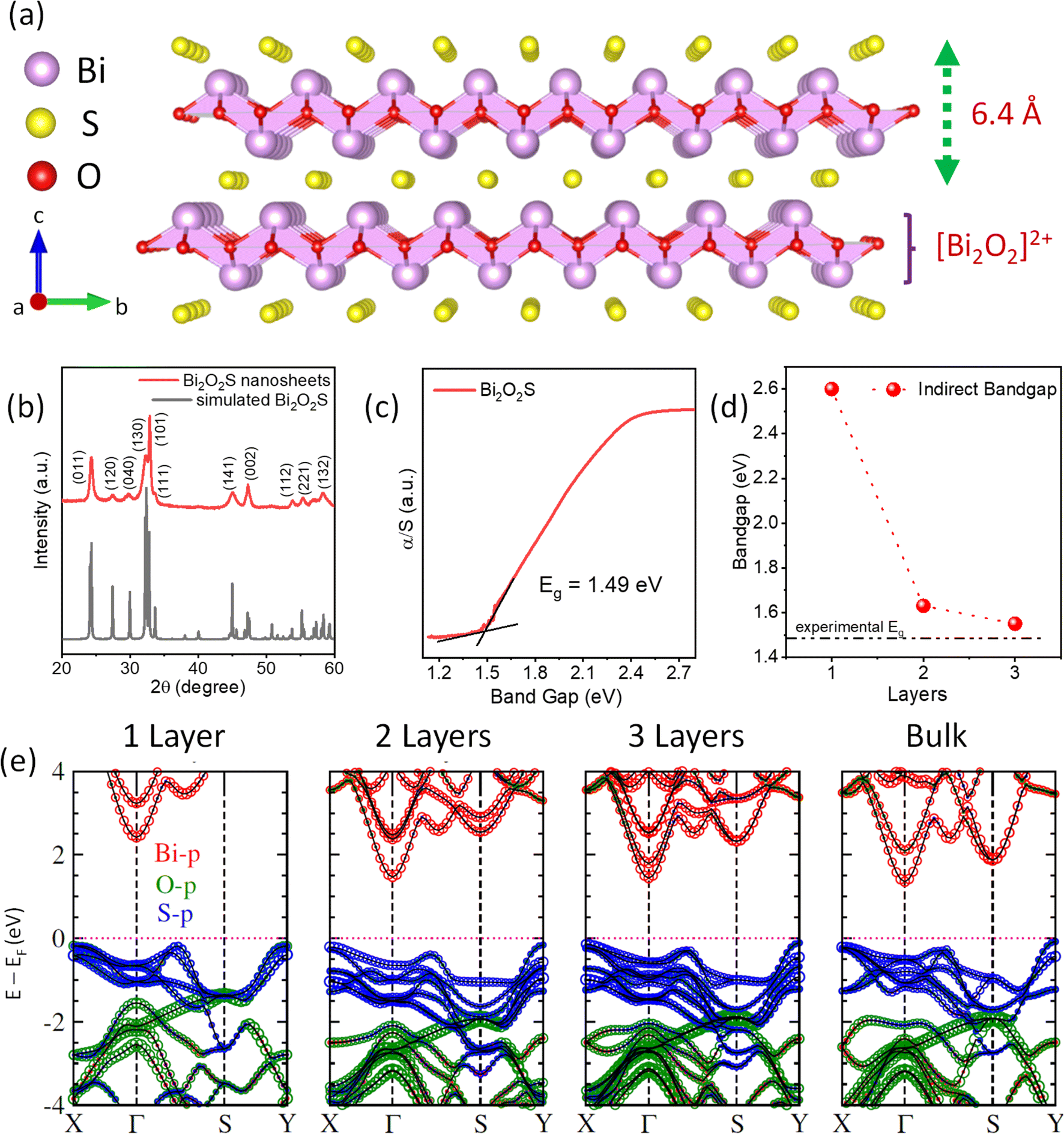 | ||
| Fig. 1 (a) Crystal structure of Bi2O2S showing the charged heterostructure layers. (b) Room temperature X-ray diffraction (XRD) pattern of the synthesized Bi2O2S nanosheets. (c) Room temperature band gap data of the synthesized Bi2O2S powders. (d) Variation of the indirect band gap with layers of Bi2O2S as per DFT calculations. (e) Electronic band structure of mono-, bi-, tri-layer and bulk Bi2O2S. | ||
Herein, we have synthesized ultrathin freestanding nanosheets of Bi2O2S via a simple, rapid, and scalable solution-based mild chemistry method at room temperature. Atomic force microscopy (AFM) studies confirm that the thickness of the sheet is nearly 2 nm, which corresponds to three layers of Bi2O2S. Transmission electron microscope (TEM) images confirm that the lateral dimensions of the nanosheets vary from 100 to 200 nm. Temperature-dependent dielectric measurement and differential scanning calorimetry (DSC) studies indicate a ferroelectric like transition at 440 K in the case of Bi2O2S nanosheets. Piezoelectric force microscopy (PFM) performed at room temperature indicates the presence of local ferroelectric domains in Bi2O2S nanosheets. PFM Dual ac Resonance Tracking Spectroscopy (PFM DART) indicates a clear signature of spontaneous polarization and its 180° switching behavior under the application of an external electric field confirms the ferroelectric nature of Bi2O2S nanosheets. To understand the underlying cause of ferroelectricity in the Bi2O2S nanosheets, we performed high resolution TEM (HRTEM) analysis and supported our findings with density functional theoretical (DFT) calculations of phonon dispersion. The observed spontaneous polarization in Bi2O2S nanosheets originates from the local distortion of Bi2O2 layers, which breaks the inversion symmetry locally. Our DFT calculations verify that each layer of Bi2O2 is ferroelectric in nature due to this spontaneous distortion. However, two consecutive layers have an antiferroelectric interaction among them owing to the polarization in the opposite direction. Thus, dipole moments are spontaneously generated for an odd number of layers in Bi2O2S, which give rise to lingering ferroelectricity in Bi2O2S nanosheets.
Results and discussions
A mild chemistry or soft chemistry or chimie douce approach has been previously utilized to synthesize many exotic non-thermodynamic phases of metal oxides and sulfides,44–46 and even recently to synthesize high entropy perovskite halide single crystals.47 Here, ultra-thin single-crystalline nanosheets of Bi2O2S were synthesized by a facile and rapid solution-based mild chemistry reaction of bismuth nitrate pentahydrate (Bi(NO3)3·5H2O) and thiourea (CS(NH2)2) (details in the ESI†) at room temperature. The nanosheets are free-standing and do not require a substrate to grow on. The total reaction time is very fast, i.e., ∼10–15 min and the reaction can be performed in a standard laboratory beaker at room temperature. In the first step, Bi(NO3)3·5H2O gets hydrolyzed in the presence of an aqueous medium to form milky white BiONO3 and the process accelerates after the addition of KOH. CS(NH2)2 was used as a precursor for sulphide ions since it can slowly release S2− ions in the basic medium. With the addition of CS(NH2)2 in the basic medium, it decomposes into sulphide ions (S2−) that react with BiONO3 to form an orange-brown coloured Bi2O2S precipitate. The reaction is scalable up to ∼1 g under ambient laboratory conditions. Thus, Bi2O2S is synthesized by bringing together [Bi2O2]2+ and S2− from two different precursors in an alkaline medium and they electrostatically combine to form Bi2O2S. We have synthesised a controlled bulk phase of Bi2O2S by a vacuum sealed-tube solid state melting reaction at 1223 K by mixing stoichiometric amounts of Bi2O3 and Bi2S3 (see the Methods in the ESI†).The room temperature powder X-ray diffraction (PXRD) pattern of the as-synthesized Bi2O2S nanosheets before vacuum drying shows a diffuse broad pattern with major peaks at 2θ ∼ 27° and 40° (Fig. S1, ESI†). The broadness and diffuse nature of the XRD peaks give us an impression of the nanocrystalline nature of the synthesized sample. After subjecting the powder to a 36 hour vacuum drying process, the peaks in the XRD pattern were easily identifiable and could be effectively matched with a simulated pattern of polycrystalline Bi2O2S (Fig. 1b). This indicates pure phase synthesis of Bi2O2S nanosheets with an orthorhombic structure (space group Pnnm). However, even after vacuum drying the peaks were substantially broad, and majority of the peaks were overlapped indicating that the nano-dimension morphology has been retained after vacuum drying. The room temperature band gap of Bi2O2S was measured to be ∼1.5 eV (Fig. 1c). We compared the experimentally obtained band gap with the DFT calculated band gap of mono-, bi- and tri-layer Bi2O2S (Fig. 1d). The valence bands are composed of p orbitals of O and S, where the latter occupy the upper position due to the difference in electronegativity and the conduction band is mainly contributed by the p orbitals of Bi (Fig. 1e). The DFT calculations also suggest that there is an enhancement of the band gap at the Γ point upon a decrease in the number of layers. This arises due to the quantum confinement and the bandgap reaches a value of 2.6 eV for monolayer Bi2O2S. With the increase in the number of layers in Bi2O2S, there is an emergence of higher energy bands along the Γ–S direction as well as the S point, resulting in the formation of an indirect band gap along this region of the Brillouin zone. Additionally, the experimental bandgap closely matches with that of trilayer Bi2O2S obtained through DFT calculations. This result hints at the possibility of the existence of nanosheets, potentially consisting of just a few layers.
To get an idea about the morphology of the synthesized Bi2O2S sample, transmission electron microscopy (TEM) and high-resolution transmission electron microscopy (HRTEM) were performed. Fig. 2a, S2a and S3a, ESI,† show the presence of Bi2O2S nanosheets. The selected area diffraction pattern (SAED) indicates the single-crystalline nature of the sheets (Fig. 2b and S2b, ESI†). The lateral dimension of the nanosheets was approximately in the range of 150–300 nm. Fig. 2c shows the HRTEM image of single crystalline Bi2O2S. The d spacing obtained in the HRTEM image is around 0.279 nm, which corresponds to the (110) plane of Bi2O2S. The nanosheets of Bi2O2S are very thin and the AFM images substantiate this claim (Fig. 2d, S4a and S5†). The thickness of the sheets is around 1.9–2 nm, which corresponds to approximately three layers of Bi2O2S confirming the thin nanosheet morphology of the synthesized sample which is further corroborated through the amplitude image (Fig. S4b, ESI†). The presence of Bi, O and S is corroborated through energy dispersive X-ray (EDX) color mapping (Fig. S3b–d†). X-ray photoelectron spectroscopy (XPS) on Bi2O2S (Fig. S6†) confirms the +3 and −2 oxidation states of Bi and S. The characteristic 1s peak of O at 532 eV was observed along with the 4f7/2 and 4f5/2 characteristic peaks of Bi at 159 eV and 164 eV, which match with the previously reported48,49 values of O2− and Bi3+. The characteristic peaks of S2−, i.e. 2p3/2 and 2p1/2, are found at 160 and 161 eV.
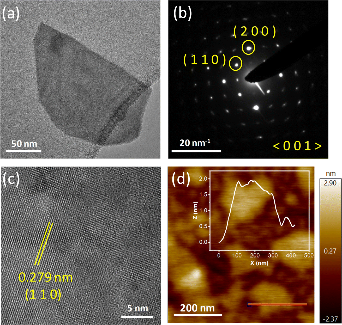 | ||
| Fig. 2 (a) Transmission electron microscopy (TEM) image of a single Bi2O2S nanosheet. (b) Selected area electron diffraction (SAED) pattern of the nanosheet along the 〈001〉 zone axis. (c) High resolution transmission electron microscopy (HRTEM) image of the nanosheet showing the (110) plane. (d) Atomic force microscopy (AFM) image of the Bi2O2S nanosheets. | ||
To gain insight into the bonding nature of the Bi2O2S nanosheets, Raman spectroscopy was conducted at room temperature and subsequently compared with its bulk counterpart (Fig. S7†). There are a few discrepancies regarding the position of Ag mode in Bi2O2S. Some research groups state that it is present above 210 cm−1, whereas others claimed that it is seen below 200 cm−1.50,51 Our results are similar to the findings of Xu et al. considering harmonic approximation.41,42,50 On further detailed analysis, it is seen that the B3g, B1g and Ag Raman peaks of Bi2O2S nanosheets (66 cm−1, 92 cm−1 and 182 cm−1, respectively) are slightly low energy shifted compared to the Raman peaks of bulk Bi2O2S. The lower energy shift in the Raman peaks can be attributed to phonon softening, resulting either from weakened interlayer coupling or an increase in strain when Bi2O2S is reduced to nano-dimensions.52,53
We have measured the temperature dependent dielectric properties of both nanosheet and bulk Bi2O2S. The real part of relative permittivity (ε′) shows a peak near 430 K without any significant dependence on the applied frequency (Fig. 3a), which can be attributed to a paraelectric to ferroelectric like transition. The maximum values of ε′ are 315, 212 and 129 at 0.25, 0.5 and 1 MHz, respectively. Further, in differential scanning calorimetry (DSC) of the nanosheet sample the peak at around Tc, ∼440 K, substantiates this claim (Fig. 3b). Interestingly, no such peak is seen in bulk Bi2O2S, suggesting that the ferroelectric ground state is stabilized when the material is synthesised in the form of 2D ultra-thin nanosheets.
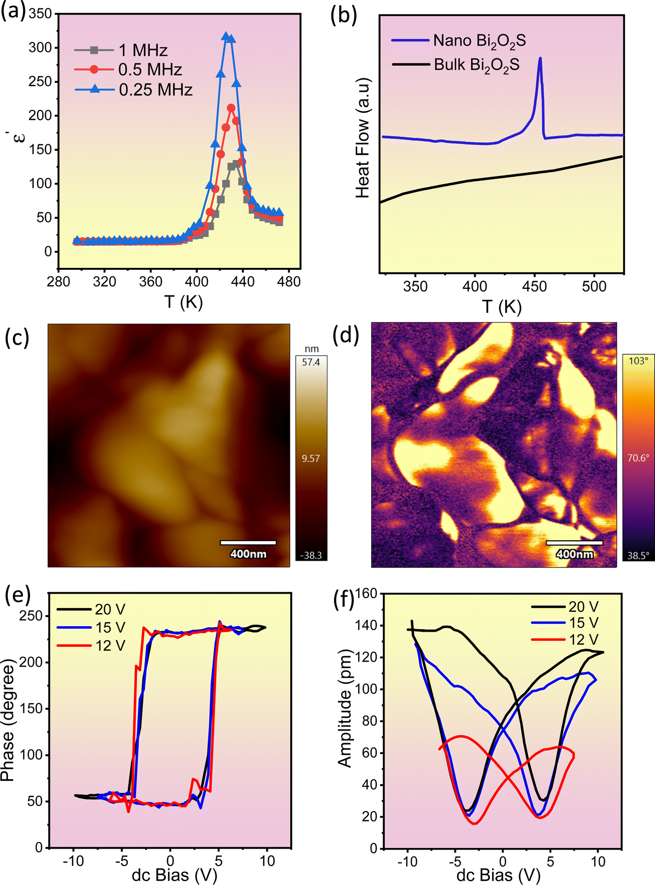 | ||
| Fig. 3 (a) Temperature variation of the real part of the dielectric constant (ε′) of Bi2O2S nanosheets at 1 MHz, 0.5 MHz and 0.25 MHz. (b) Comparative differential scanning calorimetry (DSC) data of bulk and nanosheets of Bi2O2S. (c) Topography image of drop casted Bi2O2S nanosheets. (d) Phase images of Bi2O2S nanosheets obtained through piezoelectric force microscopy (PFM). (e) Phase signal and (f) amplitude signal of Bi2O2S nanosheets obtained through switching spectroscopy PFM. | ||
To further confirm the ferroelectric instability in the 2D nanosheets, switching spectroscopy by piezoelectric force microscopy (PFM) was performed at room temperature on nanosheets of Bi2O2S. The topographic (Fig. 3c and S8a, ESI†), phase (Fig. 3d and S8b, ESI†) and amplitude images (Fig. S8c and S9, ESI†) of the Bi2O2S nanosheets indicate the presence of local ferroelectric domains within it with invariable electrical polarization. The topographic image indicates the topography or morphology of Bi2O2S nanosheets spin-coated on an indium tin oxide (ITO) substrate. The topography and phase images obtained from PFM analysis are the evidence for the existence of local ferroelectric domains with uniform electrical polarization. The occurrence in the contrast difference in the phase image denotes the occurrence of oppositely polarized local neighboring ferroelectric domains. The corresponding amplitude image (Fig. S9, ESI†) demonstrates the amplitude of the ferroelectric domains as depicted in the phase image. To further establish the presence of local ferroelectric domains in Bi2O2S nanosheets, spontaneous polarization state and switching behavior under an externally applied field were studied and the observed room temperature hysteric behavior in the “off-state” piezoelectric signal of Bi2O2S nanosheets is shown in Fig. 3e and f. The ‘off-state’ amplitude suggests the enhancement of the displacement amplitude, i.e. the electromechanical response of the sample with increase in the applied voltage. The phase of the PFM responsive signal (Fig. 3e) indicates the direction of the polarization of the nanodomains, while the amplitude of the PFM signal (Fig. 3f) indicates the magnitude of the polarization of the nanodomains. The polarization hysteresis depicted in the PFM DART phase data (Fig. 3e), which arises because of 180° switching, is the fingerprint of ferroelectric materials and involves the nonlinear increase of polarization with the electric field. The coercive field of the measured Bi2O2S nanosheets is 8 V, indicating that the energy barrier between opposite polarized states is moderately high. However, the coercive field found in Bi2O2Se nanosheets reported by Ghosh et al. is found to be 14 V (ref. 31) indicating that the ferroelectric nature in Bi2O2S is relatively weaker than that of Bi2O2Se. Additionally, this type of reorientation or switching behaviour is well known to contribute to the strain of these materials. As a result, if the electric field is cycled, a strain-electric field hysteresis loop is obtained, which resembles the shape of a butterfly as presented in the PFM DART amplitude data (Fig. 3f). The butterfly loop observed in the amplitude vs. dc bias plot indicates the ability to switch between two stable polarizable states under the influence of an external bias field, confirming the ferroelectric nature of Bi2O2S 2D nanosheets.
As mentioned earlier, bulk Bi2O2S crystallizes in a centrosymmetric space group Pnnm, so the presence of ferroelectric domains in Bi2O2S 2D nanosheets is rather surprising. Therefore, to further comprehend the origin of the observed ferroelectricity in the 2D nanosheets, density functional theory (DFT) calculations were performed for a symmetric structure (Es) as well as distorted structure (Ed), in which Bi and O/S atoms were displaced diagonally from their equilibrium positions in opposite directions. We have carried out further calculation in the Bi2O2S system by applying compressive uniaxial strain along the crystallographic a direction. The extent of the strain has been measured as ζ = (a − a0)/a0, where a and a0 are the in-plane lattice constants for the strained and pristine nanosheets, respectively. Fig. 4a and b show the variation of Es − Ed and the dipole moment with the applied uniaxial strain along the a axis for mono- to tri-layer Bi2O2S. Our calculated data show that the ferroelectricity in Bi2O2S exists for ζ > 2%, which is slightly higher than that of Bi2O2Se.31 Bulk Bi2O2S has a (BiO)2 rhombic network (D2h), which creates the [Bi2O2]2+ layer. When the dimension of Bi2O2S is diminished to the nano-regime, the strain results in the atomic displacement of Bi and O, which destroys the rhombic network locally. The destruction of the rhombic structure breaks the inversion symmetry locally in the Bi2O2S nanosheet.
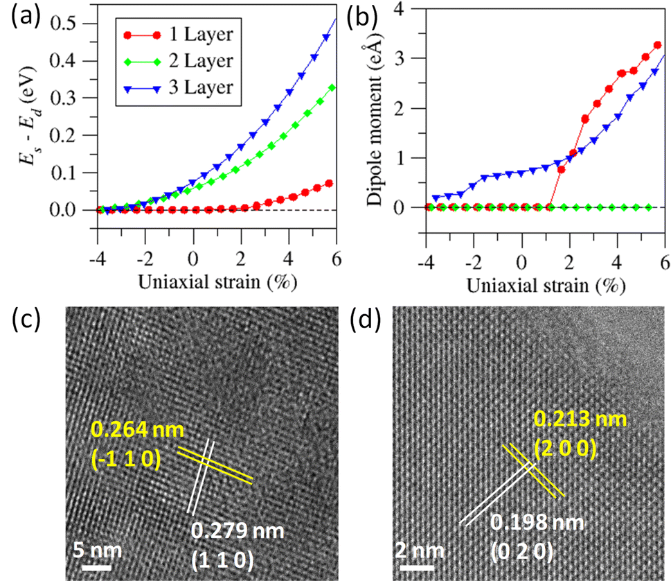 | ||
| Fig. 4 (a) Variation of Es − Ed and (b) total dipole moment under strain for monolayer, bilayer, and trilayer Bi2O2S nanosheets (Es and Ed represent the total energy for symmetrical and distorted structures, respectively). (c) and (d) HRTEM image projected along the [001] direction exhibiting deviation between interatomic distances along (110) & (−110) and (200) & (020) directions. | ||
We find that at different ζ, the values of Es − Ed are different for mono-, bi- and tri-layer Bi2O2S (Fig. 4a). Additionally, ΔE (=Es − Ed) becomes positive upon application of a minute strain (2%), indicating that the spontaneous distortion of the Bi and O atoms is energetically favourable. Interestingly, for trilayer Bi2O2S, we get a spontaneous dipole moment even in the unstrained phase, which is not seen for monolayers and bilayers indicating ferroelectric behaviour (Fig. 4b). In the case of a single layer of Bi2O2S, a small amount of strain of around 1.6% is required to stimulate ferroelectricity. For bilayers of Bi2O2S, surprisingly, the dipole moment is zero for all the calculated strain values even though there is a finite ΔE value for the bilayer. We propose that the residual dipole moment that is generated in a single layer of Bi2O2S due to the spontaneous distortion of Bi and O couples with the following layer of residual dipole moment, in an antiferroelectric manner thus producing no net dipole moment in the bilayer. Thus, an even number of layers of Bi2O2S will show no net dipole moment and an odd number of layers will show a considerable amount of ferroelectric behaviour due to the lingering dipole moment.
To verify the spontaneous local distortion experimentally, we have carried out high-resolution transmission electron microscopy (HRTEM) of Bi2O2S nanosheets. According to the orthorhombic symmetry of Bi2O2S (space group: Pnnm), the interplanar spacing (d) between the (110) and (−110) planes should be identical. However, HRTEM images show that the deviation of the interplanar distances of (110) and (−110) planes is 0.15 Å (Fig. 4c and S10a†). Similarly, the fast Fourier transformation (FFT) image (Fig. S10b†) shows the spots for (110) and (−110) planes and d110 and d−110 are non-equivalent by a distance of 0.11 Å. Thus, a visualization of the local atomic distortion is imminent, indicating a breakdown of the local symmetry in Bi2O2S nanosheets. Similarly, this distortion is also visible for (200) and (020) planes (Fig. 4d). According to the space group, Pnnm with crystallographic axes a = 3.85 Å; b = 3.89 Å and c = 11.97 Å, the ratio of d020 and d200 ideally should be 1.01:1; however the experimentally obtained ratio is 1.075:1, which is about 7% higher than the ideal scenario further confirming the local symmetry breakdown in Bi2O2S nanosheets (Fig. 4d). These spontaneous local distortions change the D2h symmetry of the Bi2O2 chains towards a C2v one generating room temperature 2D ferroelectricity in the ultrathin Bi2O2S nanosheets.
To understand the lattice dynamics in Bi2O2S nanosheets, we calculated phonon dispersion for both bulk and trilayer Bi2O2S using first-principles DFT calculations (Fig. 5). There is no trace of unstable phonon modes in bulk Bi2O2S (Fig. 5a). While we move from bulk to trilayer Bi2O2S, unstable phonon modes are observed throughout the Brillouin zone (Fig. 5b), which indicates local distortion in the nanosheet subsequently causing ferroelectric instability.54,55 Interestingly, the negative phonon modes substantially increase at the Γ point for the Bi2O2S monolayer upon the application of stress (Fig. S11, ESI†). This finding corroborates that a minute amount of strain (∼2%) was required to induce ferroelectricity in monolayer Bi2O2S (Fig. 4a). Furthermore, the unstable phonon modes in trilayer Bi2O2S are mainly contributed by the Bi and O vibrations as observed from their Eigenvector visualisation (Fig. S12, ESI†). This suggests that the distortion in the (Bi2O2)2+ unit is primarily responsible for breaking the local symmetry in the nanosheets of Bi2O2S (as visualised in HRTEM) resulting in 2D-ferroelectricity at room temperature.
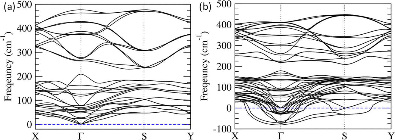 | ||
| Fig. 5 Phonon dispersion of (a) bulk Bi2O2S and (b) trilayer Bi2O2S. | ||
Conclusion
In summary, we have successfully employed a simple and easily scalable mild or soft chemistry method to synthesize ultra-thin 2D nanosheets of Bi2O2S, which can be utilised as a non-toxic and low cost alternative to the charged layered heterostructure, Bi2O2Se. These nanosheets, obtained through simple solution based synthesis at room temperature, consist of only a few layers, are free-standing, and exhibit a single-crystalline nature. Remarkably, these nanosheets exhibit ferroelectric properties at room temperature, which can be attributed to the slight atomic displacement of the Bi and O atoms in the (Bi2O2)2+ unit, thereby breaking the local inversion symmetry and causing spontaneous dipole moments. Theoretical studies have confirmed that this ferroelectric property is observed in nanosheets with an odd number of layers, as consecutive layers are coupled by an antiferroelectric interaction. This significant finding suggests that the ultra-thin 2D bismuth oxysulphide holds promise for applications in micro/nano-electronic devices in the near future.Data availability
All data are available in the manuscript and in the ESI.†Author contributions
K. B. conceived the idea and designed the study. R. P., P. D., and K. B. carried out the synthesis, structural, other characterization, and analysis of the data. K. D. carried out the theoretical calculations. A. V., A. G., T. K. M and G. S. carried out AFM and PFM studies. R. S. R. and U. K. G. carried out the TEM study. All authors contributed to writing and editing the manuscript.Conflicts of interest
There are no conflicts to declare.Acknowledgements
K. B. acknowledges financial support from the Swarnajayanti Fellowship grant, Science and Engineering Research Board (SERB) (SB/SJF/2019-20/06), DST, India. T. K. M. acknowledges the Department of Science and Technology (DST, project no. CRG/2019/005951; SPR/2021/000592) for financial support. R. P. and A. G. acknowledge JNCASR for fellowship.References
- K. S. Novoselov, A. K. Geim, S. V. Morozov, D. Jiang, Y. Zhang, S. V. Dubonos, I. V. Grigorieva and A. A. Firsov, Science, 2004, 306, 666–669 CrossRef CAS PubMed.
- H. Hong, C. Wu, Z. Zhao, Y. Zuo, J. Wang, C. Liu, J. Zhang, F. Wang, J. Feng, H. Shen, J. Yin, Y. Wu, Y. Zhao, K. Liu, P. Gao, S. Meng, S. Wu, Z. Sun, K. Liu and J. Xiong, Nat. Photonics, 2021, 15, 510–515 CrossRef CAS.
- S. Yu, X. Wu, Y. Wang, X. Guo and L. Tong, Adv. Mater., 2017, 29, 1606128 CrossRef PubMed.
- A. G. Ricciardulli, Y. Wang, S. Yang and P. Samorì, J. Am. Chem. Soc., 2022, 144, 3660–3666 CrossRef CAS PubMed.
- Z. Sun, A. Martinez and F. Wang, Nat. Photonics, 2016, 10, 227–238 CrossRef CAS.
- A. Allain, J. Kang, K. Banerjee and A. Kis, Nat. Mater., 2015, 14, 1195–1205 CrossRef CAS PubMed.
- M. Tripathi, F. Lee, A. Michail, D. Anestopoulos, J. G. McHugh, S. P. Ogilvie, M. J. Large, A. A. Graf, P. J. Lynch, J. Parthenios, K. Papagelis, S. Roy, M. A. S. R. Saadi, M. M. Rahman, N. M. Pugno, A. A. K. King, P. M. Ajayan and A. B. Dalton, ACS Nano, 2021, 15, 2520–2531 CrossRef CAS PubMed.
- W. J. Yu, Q. A. Vu, H. Oh, H. G. Nam, H. Zhou, S. Cha, J.-Y. Kim, A. Carvalho, M. Jeong, H. Choi, A. H. Castro Neto, Y. H. Lee and X. Duan, Nat. Commun., 2016, 7, 13278 CrossRef CAS PubMed.
- A. Banik and K. Biswas, Angew. Chem., Int. Ed., 2017, 56, 14561–14566 CrossRef CAS PubMed.
- P. S. Mahapatra, B. Ghawri, M. Garg, S. Mandal, K. Watanabe, T. Taniguchi, M. Jain, S. Mukerjee and A. Ghosh, Phys. Rev. Lett., 2020, 125, 226802 CrossRef CAS PubMed.
- Z. Dai, L. Liu and Z. Zhang, Adv. Mater., 2019, 31, 1805417 CrossRef CAS PubMed.
- L. Liu, Y. Li, X. Huang, J. Chen, Z. Yang, K.-H. Xue, M. Xu, H. Chen, P. Zhou and X. Miao, Adv. Sci., 2021, 8, 2005038 CrossRef CAS PubMed.
- C.-J. Liu, Y. Wan, L.-J. Li, C.-P. Lin, T.-H. Hou, Z.-Y. Huang and V. P.-H. Hu, Adv. Mater., 2022, 34, 2107894 CrossRef CAS PubMed.
- B. Tang, H. Veluri, Y. Li, Z. G. Yu, M. Waqar, J. F. Leong, M. Sivan, E. Zamburg, Y.-W. Zhang, J. Wang and A. V. Y. Thean, Nat. Commun., 2022, 13, 3037 CrossRef CAS PubMed.
- Z. Guan, H. Hu, X. Shen, P. Xiang, N. Zhong, J. Chu and C. Duan, Adv. Electron. Mater., 2020, 6, 1900818 CrossRef CAS.
- D. D. Fong, A. M. Kolpak, J. A. Eastman, S. K. Streiffer, P. H. Fuoss, G. B. Stephenson, C. Thompson, D. M. Kim, K. J. Choi, C. B. Eom, I. Grinberg and A. M. Rappe, Phys. Rev. Lett., 2006, 96, 127601 CrossRef CAS PubMed.
- D. A. Tenne, P. Turner, J. D. Schmidt, M. Biegalski, Y. L. Li, L. Q. Chen, A. Soukiassian, S. Trolier-McKinstry, D. G. Schlom, X. X. Xi, D. D. Fong, P. H. Fuoss, J. A. Eastman, G. B. Stephenson, C. Thompson and S. K. Streiffer, Phys. Rev. Lett., 2009, 103, 177601 CrossRef CAS PubMed.
- M. Wu and X. C. Zeng, Nano Lett., 2016, 16, 3236–3241 CrossRef CAS PubMed.
- W. Wan, C. Liu, W. Xiao and Y. Yao, Appl. Phys. Lett., 2017, 111, 132904 CrossRef.
- R. Fei, W. Kang and L. Yang, Phys. Rev. Lett., 2016, 117, 097601 CrossRef PubMed.
- X. Zhang, Z. Yang and Y. Chen, J. Appl. Phys., 2017, 122, 064101 CrossRef.
- W. Ding, J. Zhu, Z. Wang, Y. Gao, D. Xiao, Y. Gu, Z. Zhang and W. Zhu, Nat. Commun., 2017, 8, 14956 CrossRef CAS PubMed.
- A. Belianinov, Q. He, A. Dziaugys, P. Maksymovych, E. Eliseev, A. Borisevich, A. Morozovska, J. Banys, Y. Vysochanskii and S. V. Kalinin, Nano Lett., 2015, 15, 3808–3814 CrossRef CAS PubMed.
- M. Wu and X. C. Zeng, Nano Lett., 2017, 17, 6309–6314 CrossRef CAS PubMed.
- K. Chang, J. Liu, H. Lin, N. Wang, K. Zhao, A. Zhang, F. Jin, Y. Zhong, X. Hu, W. Duan, Q. Zhang, L. Fu, Q.-K. Xue, X. Chen and S.-H. Ji, Science, 2016, 353, 274–278 CrossRef CAS PubMed.
- Z. Fei, W. Zhao, T. A. Palomaki, B. Sun, M. K. Miller, Z. Zhao, J. Yan, X. Xu and D. H. Cobden, Nature, 2018, 560, 336–339 CrossRef CAS PubMed.
- P. Sutter, H. P. Komsa, H. Lu, A. Gruverman and E. Sutter, Nano Today, 2021, 37, 101082 CrossRef CAS.
- S. Yuan, X. Luo, H. L. Chan, C. Xiao, Y. Dai, M. Xie and J. Hao, Nat. Commun., 2019, 10, 1775 CrossRef PubMed.
- Y. Zhou, D. Wu, Y. Zhu, Y. Cho, Q. He, X. Yang, K. Herrera, Z. Chu, Y. Han, M. C. Downer, H. Peng and K. Lai, Nano Lett., 2017, 17, 5508–5513 CrossRef CAS PubMed.
- C. Zheng, L. Yu, L. Zhu, L. Collins James, D. Kim, Y. Lou, C. Xu, M. Li, Z. Wei, Y. Zhang, T. Edmonds Mark, S. Li, J. Seidel, Y. Zhu, Z. Liu Jefferson, W.-X. Tang and S. Fuhrer Michael, Sci. Adv., 2018, 4, eaar7720 CrossRef PubMed.
- T. Ghosh, M. Samanta, A. Vasdev, K. Dolui, J. Ghatak, T. Das, G. Sheet and K. Biswas, Nano Lett., 2019, 19, 5703–5709 CrossRef CAS PubMed.
- F. Wang, S. Yang, J. Wu, X. Hu, Y. Li, H. Li, X. Liu, J. Luo and T. Zhai, InfoMat, 2021, 3, 1251–1271 CrossRef CAS.
- J. Wu, C. Tan, Z. Tan, Y. Liu, J. Yin, W. Dang, M. Wang and H. Peng, Nano Lett., 2017, 17, 3021–3026 CrossRef CAS PubMed.
- J. Li, Z. Wang, Y. Wen, J. Chu, L. Yin, R. Cheng, L. Lei, P. He, C. Jiang, L. Feng and J. He, Adv. Funct. Mater., 2018, 28, 1706437 CrossRef.
- Q. Fu, C. Zhu, X. Zhao, X. Wang, A. Chaturvedi, C. Zhu, X. Wang, Q. Zeng, J. Zhou, F. Liu, B. K. Tay, H. Zhang, S. J. Pennycook and Z. Liu, Adv. Mater., 2019, 31, 1804945 CrossRef PubMed.
- J. Wu, H. Yuan, M. Meng, C. Chen, Y. Sun, Z. Chen, W. Dang, C. Tan, Y. Liu, J. Yin, Y. Zhou, S. Huang, H. Q. Xu, Y. Cui, H. Y. Hwang, Z. Liu, Y. Chen, B. Yan and H. Peng, Nat. Nanotechnol., 2017, 12, 530–534 CrossRef CAS PubMed.
- J. Han, X. Han, C. Zhang, S. Peng, C. Han, X. Zhang, X. Liu, X. Du, J. Gou and J. Wang, J. Mater. Chem. C, 2021, 9, 7910–7918 RSC.
- R. Guo, P. Jiang, T. Tu, S. Lee, B. Sun, H. Peng and R. Yang, Cell Rep. Phys. Sci., 2021, 2, 100624 CrossRef CAS.
- Z.-h. Zheng, T. Wang, B. Jabar, D.-w. Ao, F. Li, Y.-x. Chen, G.-x. Liang, J.-t. Luo and P. Fan, ACS Appl. Energy Mater., 2021, 4, 10290–10297 CrossRef CAS.
- L.-D. Zhao, S.-H. Lo, J. He, H. Li, K. Biswas, J. Androulakis, C.-I. Wu, T. P. Hogan, D.-Y. Chung, V. P. Dravid and M. G. Kanatzidis, J. Am. Chem. Soc., 2011, 133, 20476–20487 CrossRef CAS PubMed.
- B. Chitara, T. B. Limbu, J. D. Orlando, Y. Tang and F. Yan, Nanoscale, 2020, 12, 16285–16291 RSC.
- X. Yang, L. Qu, F. Gao, Y. Hu, H. Yu, Y. Wang, M. Cui, Y. Zhang, Z. Fu, Y. Huang, W. Feng, B. Li and P. Hu, ACS Appl. Mater. Interfaces, 2022, 14, 7175–7183 CrossRef CAS PubMed.
- L. Jiang, Z. Li, D. Wang, T. Guo and Y. Hu, Appl. Surf. Sci., 2022, 601, 154185 CrossRef CAS.
- J. Gopalakrishnan, Chem. Mater., 1995, 7, 1265–1275 CrossRef CAS.
- R. E. Schaak and T. E. Mallouk, Chem. Mater., 2002, 14, 1455–1471 CrossRef CAS.
- C. N. R. Rao and K. Biswas, in Essentials of Inorganic Materials Synthesis, 2015, pp. 57–95, DOI:10.1002/9781118892671.ch10.
- M. C. Folgueras, Y. Jiang, J. Jin and P. Yang, Nature, 2023, 621, 282–288 CrossRef CAS PubMed.
- P. K. Nayak, M. Sendner, B. Wenger, Z. Wang, K. Sharma, A. J. Ramadan, R. Lovrinčić, A. Pucci, P. K. Madhu and H. J. Snaith, J. Am. Chem. Soc., 2018, 140, 574–577 CrossRef CAS PubMed.
- M. M. Can, S. Ismat Shah, M. F. Doty, C. R. Haughn and T. Fırat, J. Phys. D: Appl. Phys., 2012, 45, 195104 CrossRef.
- Y.-D. Xu, C. Wang, Y.-Y. Lv, Y. B. Chen, S.-H. Yao and J. Zhou, RSC Adv., 2019, 9, 18042–18049 RSC.
- T. Cheng, C. Tan, S. Zhang, T. Tu, H. Peng and Z. Liu, J. Phys. Chem. C, 2018, 122, 19970–19980 CrossRef CAS.
- J. M. Wesselinowa and S. Kovachev, Phys. Rev. B: Condens. Matter Mater. Phys., 2007, 75, 045411 CrossRef.
- Y. Gao, X. Zhao, P. Yin and F. Gao, Sci. Rep., 2016, 6, 20539 CrossRef CAS PubMed.
- A. Banik, T. Ghosh, R. Arora, M. Dutta, J. Pandey, S. Acharya, A. Soni, U. V. Waghmare and K. Biswas, Energy Environ. Sci., 2019, 12, 589–595 RSC.
- D. Sarkar, T. Ghosh, S. Roychowdhury, R. Arora, S. Sajan, G. Sheet, U. V. Waghmare and K. Biswas, J. Am. Chem. Soc., 2020, 142, 12237–12244 CrossRef CAS PubMed.
Footnote |
| † Electronic supplementary information (ESI) available. See DOI: https://doi.org/10.1039/d4sc00067f |
| This journal is © The Royal Society of Chemistry 2024 |