
 Open Access Article
 This Open Access Article is licensed under a Creative Commons Attribution-Non Commercial 3.0 Unported Licence
Nanoparticle-directed bimodal crystallization of the quasi-1D van der Waals phase, Bi4I4†
Steven Jay
Allison
 a,
Dmitri Leo Mesoza
Cordova
a,
Maham
Hasib
a,
Toshihiro
Aoki
b and
Maxx Q.
Arguilla
*a
a,
Dmitri Leo Mesoza
Cordova
a,
Maham
Hasib
a,
Toshihiro
Aoki
b and
Maxx Q.
Arguilla
*a
aDepartment of Chemistry, University of California Irvine, Irvine, California 92697, USA. E-mail: marguill@uci.edu
bIrvine Materials Research Institute, University of California Irvine, Irvine, California 92697, USA
First published on 19th February 2024
Abstract
Anisotropy often yields unexpected structures and properties in the solid state. In van der Waals (vdW) solids comprised of 1D or quasi-1D (q-1D) building blocks, anisotropy in both intra- and inter-chain directions results in an abundance of crystalline packing motifs and drastically altered physical states. Among these, structurally and chemically complex 1D/q-1D vdW solids that display topologically protected states, unique optical properties, and enhanced electrical transport properties in 1D are sought after owing to their potential as building blocks for next-generation quantum devices that approach the sub-nanometer regime. Yet, the access to such facet- and edge-specific physical states is still limited by the stochastic nature of micromechanical exfoliation. Here, we demonstrate that the representative Bi4I4 phase, an established pnictohalide q-1D vdW topological insulator in the bulk, can be crystallized from the vapor phase either into well-defined nanowires or quasi-2D nanosheets. We find that gold nanoparticles (Au NPs) on the growth substrate, in conjunction with the highly anisotropic structure of Bi4I4 common to many q-1D vdW crystals, direct the dimensionality of high-purity Bi4I4 nanostructures. Systematic variation of Au NP diameters, Bi![[thin space (1/6-em)]](https://www.rsc.org/images/entities/char_2009.gif) :I precursor ratios, and growth-deposition temperatures reveal that Au NPs generally act as nucleation sites for vapor–solid (VS) growth of Bi4I4 nanowires. Strikingly, post-synthesis analyses of the elemental composition of 20 nm Au NPs on the substrate surface show an equisotichiometric 1:1 ratio of Bi to I within the Au NP that triggers the vapor–liquid–solid (VLS) growth of [001]-oriented quasi-2D nanosheets comprised of laterally-ordered [Bi4I4]n chains along the perpendicular [100] direction. We rationalize the observed bimodal growth pathways and the morphologically distinct nanostructures based on crystallization habits and orientations of the nanostructures, Bi:I ratios in the resulting Au NPs post-synthesis, and the orientation of stereochemically active Bi lone pairs between adjacent chains. We anticipate that these growth pathways are adaptable to the synthesis of emergent halide- and chalcogen-based 1D vdW nanocrystals with diverse physical and quantum properties.
:I precursor ratios, and growth-deposition temperatures reveal that Au NPs generally act as nucleation sites for vapor–solid (VS) growth of Bi4I4 nanowires. Strikingly, post-synthesis analyses of the elemental composition of 20 nm Au NPs on the substrate surface show an equisotichiometric 1:1 ratio of Bi to I within the Au NP that triggers the vapor–liquid–solid (VLS) growth of [001]-oriented quasi-2D nanosheets comprised of laterally-ordered [Bi4I4]n chains along the perpendicular [100] direction. We rationalize the observed bimodal growth pathways and the morphologically distinct nanostructures based on crystallization habits and orientations of the nanostructures, Bi:I ratios in the resulting Au NPs post-synthesis, and the orientation of stereochemically active Bi lone pairs between adjacent chains. We anticipate that these growth pathways are adaptable to the synthesis of emergent halide- and chalcogen-based 1D vdW nanocrystals with diverse physical and quantum properties.
Introduction
Encoding structural and electronic complexity in solids typically relies on the precise control of anisotropies that exist across various length scales. In 2D vdW crystals, an understanding of the interplay between anisotropic bonding interactions and crystalline symmetry has led to the discovery of numerous unusual physical behaviors in the bulk and down to the single layer, including: 2D topological states and the quantum spin Hall effect,1–3 unusual superconductivity arising from moiré states,4 strong spin-valley coupling,5 Wigner crystals,6 and goniopolarity.7 This notion of confining well-defined physical states in 2D, enabled by stable, atomically precise surfaces, has further inspired the search towards low-dimensional solids that could host highly confined 1D states approaching the single chain regime.In currently established 2D vdW crystals, electronic or optical states in 1D are often accessed via 2D lattices that bear an underlying 1D motif such as in phosphorene,8,9 or through bottom-up routes which direct the growth of transition metal dichalcogenide lattices into their 1D counterparts by disrupting the formation of in-plane covalent bonds through substrate and growth engineering,10,11 catalyzed VLS growth,12–14 artificial step edges,15 or growth inside carbon nanotubes.16 Owing to their structural resemblance to 2D vdW crystals, crystalline phases comprised of sub-nm thick 1D or quasi-1D (q-1D, referring to chain-like structures that have non-isotropic cross-sections) chains held together by weak vdW forces have become the subject of recent attention as an alternative pathway towards solids in lower dimensions.17–22 The vdW interactions that hold the 1D/q-1D subunits together in these phases have enabled not only the direct translation of micromechanical and solution-phase exfoliation techniques developed for their 2D counterparts,23–25 but also the realization of nascent electronic, optical, and quantum states arising from 1D confinement.18,20,21,26,27 Uniquely, the existence of inter-chain vdW interactions in these phases gives rise to varying degrees of vdW interactions depending on the crystallographic orientation of the constituent chains in the basal plane.23 This is in stark contrast to the equivalent vdW interactions that hold together adjacent sheets in 2D vdW phases. While this can result in a random distribution of nanostructures of varying sizes and dimensionalities upon exfoliation, it presents an opportunity to grow nanostructures of different dimensionalities (e.g. single chain, nanowire bundles, nanoribbons, and flat or corrugated quasi-2D nanosheets) and physical properties from the same 1D/q-1D building blocks.
Encouragingly, recent work involving Sb2S3, a q-1D vdW phase and the only line compound in the Sb–S binary phase system, showed that the size and dimensionality of q-1D vdW nanostructures can be reliably controlled by tuning the ratio of precursors in the vapor phase.28 However, for binary 1D/q-1D vdW crystal systems that form more than one stoichiometric line compound, variations in the vapor phase precursor composition would have the undesirable consequence of growing competing phases. To this end, the Bi4X4 (X = Br, I) crystal system is an example of a model phase that can be employed to understand the synthetic parameters that can lead to the pure and controllable synthesis of 1D/q-1D vdW nanocrystals with various competing line compounds. This opportunity arises from the rich phase space of the Bi-X binary systems. In particular, in the Bi–I system, non-q-1D vdW phases including Bi9I7, Bi7I2, and BiI3 can compete with the bottom-up synthesis of Bi4I4.29 The dimensionally rich phase space of the Bi-X system is not unique and is also apparent in other 1D/q-1D vdW crystals with emergent physical properties, necessitating the need to develop growth strategies to selectively direct the synthesis of phase-pure 1D/q-1D vdW nanocrystals. For example, in the Nb–S binary system, competing phases of various dimensionalities such as NbS (3D covalent), NbS2 (2D vdW), and NbS3 (1D vdW) are also present in the phase space.29
Beyond their suitability as model phases for bottom-up growth of complex and dimensionally-resolved q-1D vdW nanostructures, bismuth halide crystals are of particular interest due to recent studies that experimentally demonstrated both weak and higher-order topological insulating (HOTI) behavior in these crystals.21,30–36 In these studies, the topological nature of bismuth halide phases has been shown to strictly originate from the precise orientation and stacking of the q-1D [Bi4X4]n subunits in the bulk crystal and its exposed facets. This, among the many emergent 1D/q-1D vdW crystals with size-, dimensionality-, and orientation-dependent properties, further warrants the need to understand the growth principles that underpin the controlled crystallization of well-defined 1D/q-1D vdW nanocrystals from bottom-up routes. Whereas significant developments have been made in the bottom-up synthesis of well-defined 2D vdW nanocrystals, very little has been known about the chemistry that governs the growth and crystallization behavior of 1D/q-1D vdW phases from the bottom-up.
Here, we report the vapor phase synthesis of nanowires and quasi-2D nanosheets derived from the model quasi-1D vdW phase, Bi4I4. Note that the quasi-2D terminology described herein refers to the 2D-like nanosheets formed by the side-by-side crystallization of q-1D [Bi4I4]n chains and not the 2D covalently bound sheets found in 2D vdW crystals like graphene or MoS2. We establish that the crystallization of pure and dimensionally resolved Bi4I4 nanostructures from the vapor phase is mediated by overcoming the formation of the iodine-rich BiI3 competing phase through the precise control of precursor ratios or the use of growth substrates embedded with Au NPs. Holding all other variables constant and only changing the diameter of the Au NPs, we show that the density of nanosheet growth can be increased drastically, producing hundreds of large-area quasi-2D nanosheets in the presence of 20 nm Au NPs. These quasi-2D nanosheets uniquely display a [001] crystallographic orientation, which may provide a suitable platform to observe the predicted HOTI hinge states that lie along the major (001) facet of the α-Bi4I4 phase in future studies. Using the observed nanocrystalline morphologies and crystal faceting habits of Bi4I4 which are comparable to other 1D/q-1D vdW crystals, we found that these nanostructures undergo a bimodal crystallization pathway which originates from the intrinsic q-1D vdW crystal structure and the diameter of the Au NP used in the reaction. These results, expected to be applicable to other 1D and q-1D vdW solids, underscore the role of the interplay between composition, bonding interactions, and underlying crystalline anisotropies in the creation of q-1D vdW nanostructures with diverse sizes, morphologies, and dimensionalities.
Results and discussion
In this study, we use Bi4I4 as a model phase to demonstrate the creation of well-defined nanostructures based on a q-1D vdW bismuth halide (Fig. 1A). Bi4I4 is characterized by covalent chains of [Bi4I4]n held together by weak inter-chain vdW interactions.37 Chains of Bi4I4 can crystallize into two distinct phases with slightly altered stacking motifs as a result of the weak interactions that bind the chains. Both polymorphic phases form in the base centered C12/m1 space group (No. 12), but differ in the size of the unit cell due to stacking differences.30 The β-Bi4I4 phase, whose unit cell is comprised of two [Bi4I4]n chain blocks, has been shown to be stable for temperatures above 295 K.30 The α-Bi4I4 phase is stable below 295 K and has four [Bi4I4]n chain blocks in the unit cell, effectively doubling the unit cell size. Our choice of this model phase to demonstrate the bottom-up crystallization of q-1D vdW bismuth halide nanostructures stems from unsuccessful attempts at growing the closely related Bi4Br4 phase whose syntheses were severely inhibited by air and humidity sensitivity.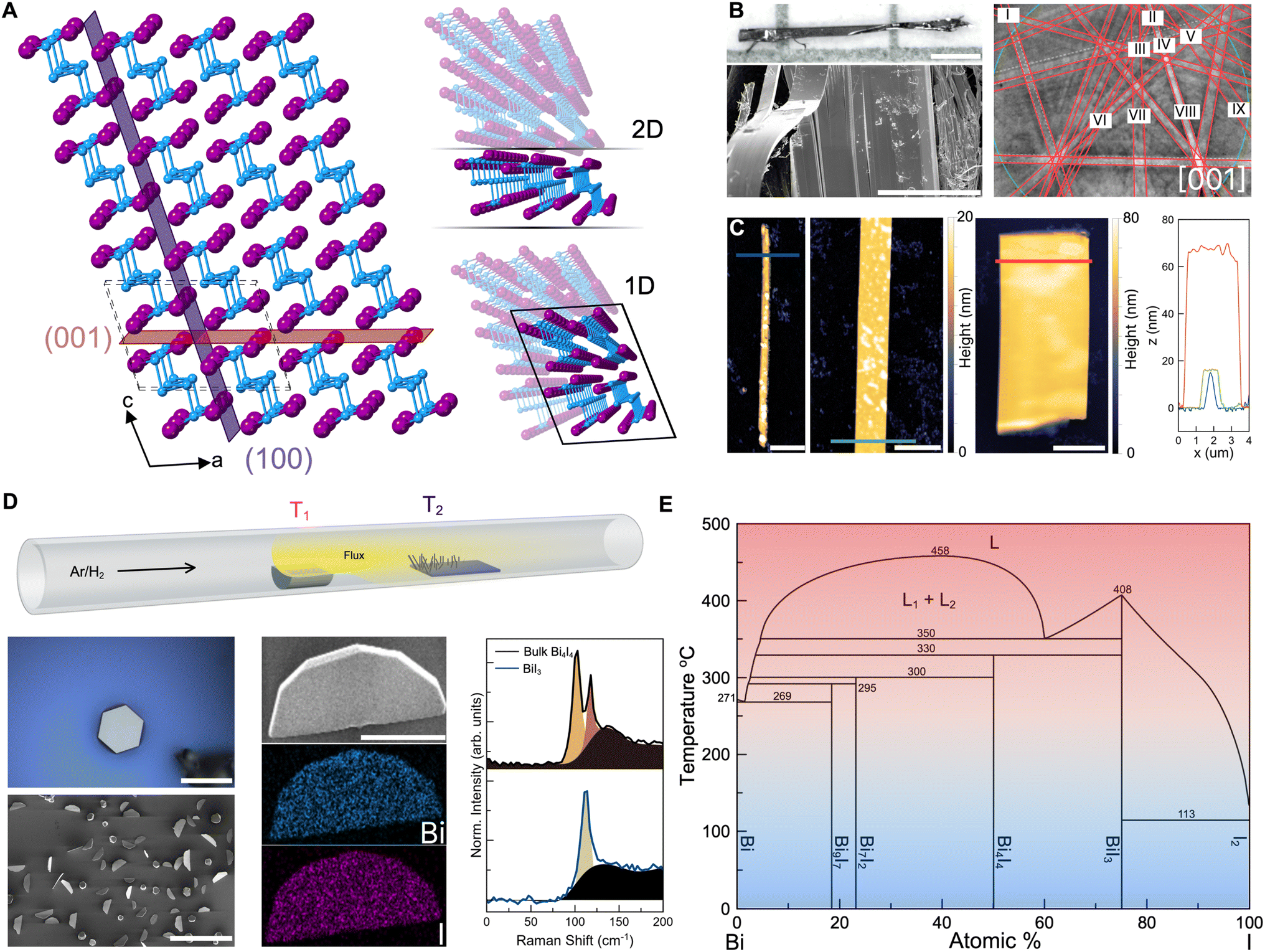 | ||
| Fig. 1 Top-down and bottom-up routes towards highly anisotropic Bi4I4 nanostructures. (A) Crystal structure representation of β-Bi4I4. Highlighted are two common planes of cleavage arising from vdW interactions that could lead to quasi-2D sheets or 1D bundles. The unit cell is depicted in dashed lines. (B) Optical (top) and SEM (bottom) image of a CVT-grown bulk Bi4I4 crystal. Scale bars: 0.5 mm (optical) and 50 μm (SEM). The EBSD pattern taken from the depicted crystal in the SEM image is shown in the left panel. Kikuchi lines are overlaid with red guide lines, the zone axis is [001]. Roman numerals correspond to the following Kikuchi lines: I 0-31, II 103, III 1-12, IV 102, V 112, VI 1-21, VII 1-11, VIII 101, and IX 111. (C) AFM of exfoliated Bi4I4 nanowires and nanoribbons from a bulk crystal. The color-matched AFM height profiles taken from line cuts in the micrograph are in the right panel. Scale bars, 2 μm. (D) Top schematic of the CVD set-up used in the study. The source (T1) and deposition (T2) zones are labeled accordingly. (D) bottom optical image, SEM image, EDS maps, and Raman spectroscopy of the CVD-grown BiI3 side product, Ag phonon mode at 113.9 cm−1.38 The Raman spectrum of bulk Bi4I4 is included for comparison, phonon modes Bg at 100.0 cm−1 and Ag at 115.9 cm−1.39 Fits of the constituent peaks and background (black) are included in each spectrum. Scale bars: 25 μm (optical), 150 μm (low-mag. SEM), 10 μm (high-mag. SEM and EDS). (E) Binary Bi–I phase diagram showing the various BixIy line compounds.29 | ||
Through chemical vapor transport (CVT), Bi4I4 grows as sizeable single crystals up to centimeters in length (Fig. 1A and B). Due to the vdW interactions that bind together chains of Bi4I4, bulk crystals are exfoliable along the [100] and [001] directions (Fig. 1A, right panel). Micromechanical exfoliation of bulk crystals resulted in nanostructures with various morphologies, thicknesses, and aspect ratios due to the various cleavable axes (Fig. 1C). Atomic force microscopy (AFM) images of these nanostructures demonstrate that nanowires, quasi-2D nanoribbons, and quasi-2D nanosheets with thicknesses in the range of 15 to 70 nm can be derived from exfoliation. Yet, while there are occasional well-defined nanocrystals, obtaining these nanowires and quasi-2D nanoribbons/nanosheets via exfoliation remains a stochastic process which yields an inconsistent distribution of nanostructures. It is important to note that the random nature of micromechanical exfoliation is more pronounced in 1D and q-1D vdW crystals compared to 2D vdW crystals, as a consequence of having weak vdW interactions across multiple crystallographic axes.
Bottom-up synthesis of phase pure Bi4I4 nanostructures
Synthesizing Bi4I4 nanocrystals via a bottom-up strategy enabled us to tune parameters such as precursor Bi-to-I ratios and synthesis temperatures to reliably obtain well-defined nanostructures (Fig. 1D and S1†). In our CVD setup, stoichiometric Bi and HgI2 powders were vaporized and transported by Ar/H2 (5%) carrier gas to a 6 cm-long, 300 nm substrate. The Ar/H2 (5%) formulation used in this study provides a mildly reducing atmosphere to help prevent the oxidation of both the precursors and the resulting nanocrystals at elevated temperatures.40 In a control CVD reaction run with pure Ar as carrier gas, no difference was observed in the growth morphologies and deposition densities of the Bi4I4 nanostructures (Fig. S2A and B†). The long growth substrate allowed for a wide temperature range, about 175 °C to 250 °C, providing an extensive window of reaction conditions (Table S1 and Fig. S2C†). For conditions similar to the CVT growth of Bi4I4 previously described in literature, iodine species from HgI2 react with and transport Bi in the vapor phase. However, reaction conditions that are similar to the CVT growth of bulk Bi4I4 crystals resulted in the uniform growth of only hexagonal BiI3 nanocrystals across the substrate.41 As a reference for subsequent reactions, we confirmed the identity of BiI3 through the expected hexagonal crystal faceting observed in scanning electron microscopy (SEM), iodine-rich 1:3 Bi-to-I ratios obtained from energy dispersive X-ray spectroscopy (EDS), and the characteristic BiI3 phonon mode at 113.9 cm−1 (Fig. 1D, bottom and Table S2†).38 The formation of BiI3, even while using stoichiometric (1:1 or 4:4) Bi:I loading, indicates that a relatively low concentration of Bi reaches the growth substrate from the vapor phase as compared to the more volatile iodine species from HgI2. This is because a multitude of BixIy compositional phases compete with the growth of Bi4I4 (Fig. 1E).29 Notably, in the iodine-rich side of the phase diagram, the only competing phase is BiI3. This suggests that increasing the concentration of Bi in the deposition zone would suppress the crystallization of BiI3.
To promote the localization of Bi atoms and induce Bi4I4 nucleation points along the growth substrate, we dropcasted 100 nm diameter gold nanoparticles (Au NPs) on the growth substrate prior to synthesis. We hypothesized that the Au NPs would preferentially dissolve Bi over I as Bi and Au form a eutectic mixture.42 Through this route, it is also possible for the Au NPs to act as a catalyst for vapor–liquid–solid (VLS) growth, a pathway commonly used in the synthesis of nanowires with isotropic covalent bonding, such as in silicon.43–46 VLS has recently been used to direct the synthesis of 2D vdW materials10,13,14,47,48 and topological insulator nanowires,49–51 but this technique has not been fully developed for 1D/q-1D vdW phases. Consistent with the Au–Bi phase diagram,42 EDS of the resulting 100 nm Au NPs from a stoichiometric (1:1 or 4:4) Bi:I loading using the same precursor temperature (T1 = 300 °C) typically used in the CVT growth of bulk Bi4I4 confirmed that Au NPs dissolved Bi more than I. EDS of these resulting nanoparticles showed varied compositions AuxBiyIz where y > z (Table S3†).
This increased solvation of Bi was observed alongside the growth of a number of amorphous and non-uniform wire-like nanostructures (Fig. 2A and S3†). EDS analysis of these non-uniform nanowire-like structures yielded a Bi-rich phase of approximately 3:1 Bi-to-I ratio (BixIy (x/y ≈ 3) or “Bi3I”; Table S4†). These Bi-rich nanostructures were found alongside BiI3 nanostructures found to have EDS ratios of 1:3 as well as a characteristic Raman shift at 117 cm−1 (Table S4 and Fig. S3†). We attribute the formation of the amorphous BixIy (x/y ≈ 3) to the conservation of mass, with “Bi3I” forming from Bi and I left over from the growth of BiI3 from a 4:4 Bi:I precursor loading. We also found, for the first-time, evidence of the formation of a small number of ∼10 μm-long nanowires with a 4:4 Bi-to-I ratio (Table S4†). The compositional variation of the resulting nanostructures indicates that Au NPs only aid in the deposition of vapor phase precursors and increase the localized concentration of precursors on the substrate surface.
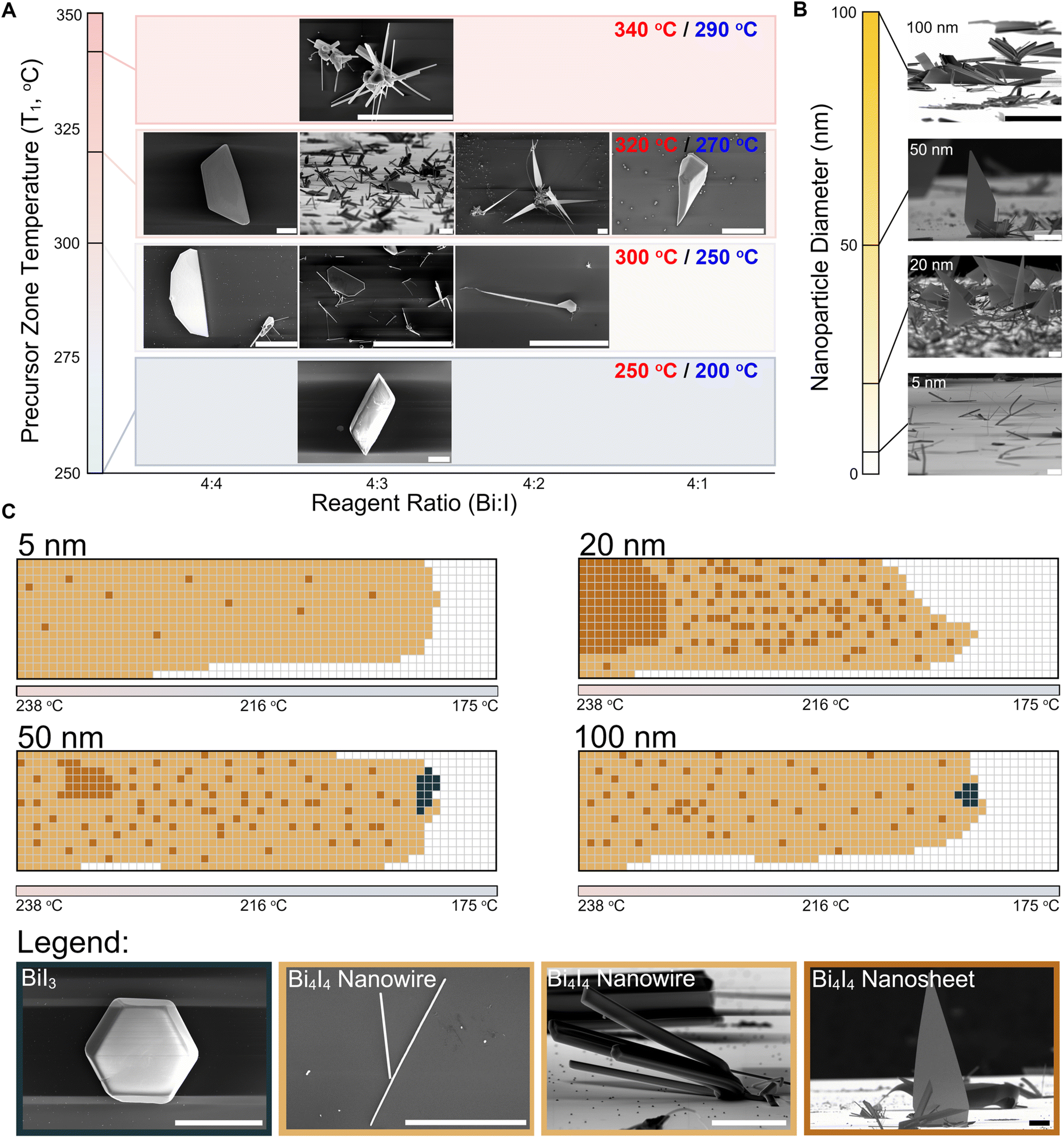 | ||
| Fig. 2 CVD growth of Bi4I4 nanostructures in the presence of Au NPs. (A) Optimization of the precursor zone temperatures and Bi:I precursor ratios in reactions with 100 nm Au NPs on the growth substrate. SEM images of the resulting nanocrystals are shown. The growth zone temperature (blue label) is also indicated at each precursor zone temperature (red label). Colors in the diagram correspond to the temperature gradient colors in the binary phase diagram in Fig. 1E. Scale bars, 10 μm. (B) Influence of the on-substrate Au NP diameters on the morphology and size of Bi4I4 nanocrystals (Reaction conditions: T1 = 320 °C/T2 = 270 °C; 4:3 Bi:I precursor ratio). Scale bars, 20 μm. (C) Mapping of the nanostructures observed in the post-synthesis substrates from reactions involving various Au NPs diameters (5 nm, 20 nm, 50 nm, and 100 nm) as shown in (B). Each box is a 1 mm × 1 mm region on the substrate. Calibrated temperatures are shown across the substrate maps. Legend: crystals of BiI3, large and small Bi4I4 nanowires, and Bi4I4 quasi-2D nanosheets are depicted in black, light brown, and dark brown boxes, respectively. White boxes correspond to regions where no discernible nanocrystal growth was observed. Scale bars from left to right: 20 μm, 40 μm, 80 μm, and 20 μm. | ||
To address the persistent formation of both the amorphous Bi-rich and crystalline I-rich side-phases, we systematically tuned the Bi and I ratios in the precursor loading and the temperatures of the precursor and growth zones (T1 and T2 in Fig. 1D, respectively). This variation, in conjunction with the presence of 100 nm Au NPs on the substrate, enabled us to determine the optimal conditions for phase pure growth of Bi4I4 nanostructures (Fig. 2A). A precursor/growth zone temperature setting of T1 = 320 °C/T2 = 270 °C and a Bi:I loading ratio of 4:3 produced a dense growth substrate dominated by Bi4I4 nanocrystals with minimal BiI3 growth (Fig. 2A and S4†). Conditions outside of these optimal parameters provided us insights on the growth patterns of the various crystalline BixIy species from the vapor phase (Fig. 2A, ESI†).
The identities of the crystalline phases were confirmed by Raman spectroscopy (Fig. S3 and S5†) and grazing incidence X-ray diffraction (GI-XRD), and the elemental compositions were determined by EDS (Table S5†). GI-XRD confirms the purity, dense substrate coverage, and ensemble crystal structure. The experimental diffractogram overlaid with the simulated powder diffraction pattern corresponds with the β-Bi4I4 phase. Bi4I4 crystals were characterized as having Raman shifts at 100.0 cm−1 and 115.6 cm−1 (matching well to previously reported Bi4I4 phonon modes)39 and 4:4 Bi-to-I EDS ratios. BiI3 crystals were characterized as having Raman shifts from 115–117 cm−1 (corresponding to previously reported BiI3 phonon modes)38,52 and 1:3 Bi-to-I EDS ratios. “Bi3I” nanoparticles with 3:1 Bi-to-I composition were amorphous and gave no Raman signal. Optimal conditions not only yielded generally phase pure Bi4I4 nanostructures, but also produced nanocrystalline morphologies not previously seen in the micromechanical exfoliation of bulk crystals (Fig. 1C). We observed both nanowires and, surprisingly, triangular quasi-2D nanosheets. Tilted (90°) SEM micrographs show the quasi-2D nanosheets are 100–200 μm in length and 50–75 μm in width (Fig. 2A and B), with thicknesses in the range of 100–200 nm as measured by AFM (Fig. S6†). These morphologies and dimensions are far different from any observed nanostructures of Bi4I4, underscoring the uniqueness of the quasi-2D growth of a q-1D vdW nanocrystal.
As Au NPs have been used to constrain crystal size and to control dimensionality in 2D and 3D crystalline systems, we also probed the effect of Au NP size on the growth of Bi4I4 nanostructures. As we decreased the Au NP diameter from 100 nm to 50 nm to 20 nm, we found that the density of quasi-2D nanosheets on the growth substrate increased precipitously (Fig. 2B). Yet, as the size of the nanoparticle was decreased still further to 5 nm, little to no nanosheets were observed. SEM images taken at a 90° tilt illustrate the effect of Au NP diameter on growth density and crystal morphology of the resulting nanostructures (Fig. 2B).
Our CVD methodology enabled us to map out, with 1 mm2 resolution, the temperature- and precursor distance-dependence of the nanostructures grown on the substrate (Fig. 2C). From these panoramic substrate maps, for all Au NP diameters, we generally observed the formation of nanowire structures (depicted in light brown; Fig. 2C) across the length of the substrate. In larger Au NP diameters with 50 nm and 100 nm diameters, BiI3 nanocrystals (depicted in black; Fig. 2C) were still apparent but were found only in trace amounts towards the far end of the substrate. This is consistent with the expected higher concentration of the more mobile iodine atoms in the vapor phase precursors and the possibility of bismuth atom depletion at the surface of the substrate due to the greater volume of Au NPs upstream in the 50 and 100 nm Au NP loadings which we discuss in detail in the ESI† in the latter section of the manuscript (Fig. S15 and Table S13†). This depletion of Bi in the vapor phase, which to some extent is unlikely due to the constant flux of precursors for the short duration (∼5 minutes) of each CVD reaction, may have influenced the ratios of Bi and I available and thus have resulted in the growth of BiI3 observed towards the end of the substrate in the 50 nm and 100 nm diameter Au NP reactions (Fig. 2C). Contrastingly, we observed that the quasi-2D nanosheets grew most densely in the hotter regions of the substrate that were in closer proximity to the precursor boat (depicted in dark brown; Fig. 2C). While quasi-2D nanosheets were occasionally observed in reactions with 50 nm and 100 nm diameter Au NPs, the growth of Bi4I4 quasi-2D nanosheets occurred at a far greater density in growths that involved Au NPs with 20 nm diameter, yielding roughly 30–50 flakes per 1 mm2 area. While the diameters of the Au NPs appeared to control the purity, dimensionality, and density of as-grown nanostructures, it had minimal influence on the size of these nanostructures. Significant Au NP size-driven effects were only apparent in Bi4I4 nanostructures grown using Au NPs with 5 nm diameters (Fig. 2B).
Structural characterization of Bi4I4 nanostructures
We evaluated the structure, morphology, and crystalline quality of the two distinct Bi4I4 nanostructures that emerged from our syntheses (Fig. 3). From SEM and transmission electron microscopy (TEM) imaging, we found that the optimized growth parameters yielded well-defined nanowires (Fig. 3A and E) and nanosheets (Fig. 3H and L). We observed that nanowires generally crystallize and protrude from localized nucleation points along the length of the substrate. These nanowires extend outward from these nucleation spots in a radial growth pattern, a crystallization habit commonly observed in bulk crystals that feature 1D or q-1D like substructures (Fig. 3A). Unlike nanowires traditionally grown via VLS,43,45,46 we did not observe any Au NPs, distinct grain boundaries, or discontinuities at the ends of these nanowires (Fig. S4†). These observations contrast with that of the nanosheets which laterally grow from nanowires protruding from the substrate. These nanosheets display a flag-like triangular morphology that converges to a sharp point with an Au NP at the tip (Fig. 3H and S4†).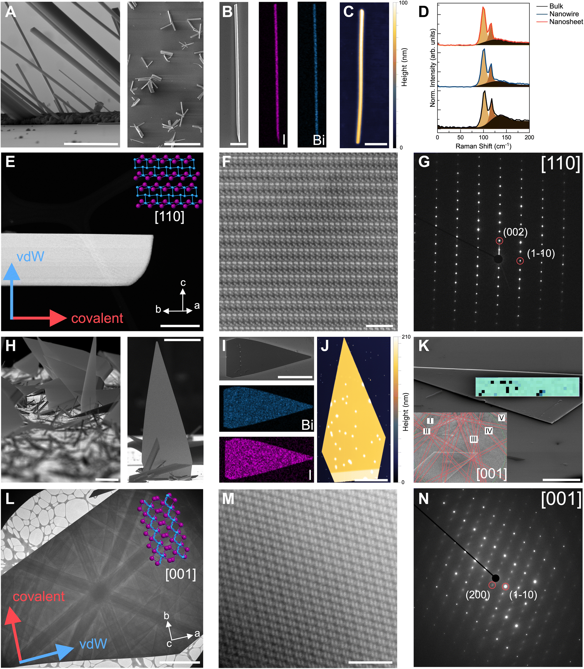 | ||
| Fig. 3 Structural characterization of Bi4I4 nanostructures. (A) High-magnification (left) and low-magnification (right) SEM images of representative Bi4I4 nanowires. Scale bars, 2 μm (left) and 50 μm (right). (B) SEM image and Bi (Mα line) and I (Lα line) elemental maps from EDS of a Bi4I4 nanowire. Scale bar, 10 μm. (C) AFM of an 87 nm-thick nanowire. Scale bar, 1 μm. (D) Raman spectra of CVD-grown Bi4I4 nanowire, quasi-2D nanosheet, and bulk Bi4I4 crystal. Phonon modes are Bg at ∼100 cm−1 and Ag at ∼115 cm−1.39 Fits of the constituent peaks and the background (black) are included in each spectrum. (E) Low-magnification TEM image of Bi4I4 nanowire with the corresponding crystallographic orientation and crystal structure. The covalent axis is parallel to the long axis of the wire. Scale bar, 200 nm. (F) High-magnification HAADF-STEM image of the Bi4I4 nanowire in (E). Scale bar, 2 nm. (G) SAED of the nanowire in (E) which is indexable to the [110] zone axis of β-Bi4I4 polytype. (H) High-magnification (left) and low-magnification (right) SEM images of representative Bi4I4 nanosheets. Scale bars, 20 μm (left) and 50 μm (right). (I) SEM image and Bi (Mα line) and I (Lα line) elemental maps from EDS of a Bi4I4 nanosheet. Scale bar, 50 μm. (J) AFM of a 149 nm-thick nanosheet. Scale bar, 10 μm. (K) EBSD map and corresponding Kikuchi pattern (inset) of a [001]-oriented single-crystalline Bi4I4 quasi-2D nanosheet. Scale bar, 10 μm. Roman numerals correspond to the following Kikuchi lines: I 0-2-1, II 0-3-1, III -1-2-1, IV -1-1-1, and V -10-1. The black pixels in the map are attenuated EBSD signals. (L) Low-magnification TEM image of Bi4I4 nanosheet with the corresponding crystallographic orientation and crystal structure. The covalent axis is perpendicular to the long axis of the nanosheet. Scale bar, 2 μm. (M) High-magnification HAADF-STEM image of the Bi4I4 nanosheet in (L). Scale bar, 2 nm. (N) SAED of nanosheet in (L) which is indexable to the [001] zone axis of β-Bi4I4 polytype. | ||
EDS spectroscopy and mapping of both the nanowires (Fig. 3B) and the nanosheets (Fig. 3I) showed uniform, 4:4, Bi-to-I ratio and distribution across the nanostructures, indicating phase purity and elemental uniformity (Table S5†). AFM micrographs of mechanically transferred nanowires and nanosheets show well-defined edges and smooth surfaces with thicknesses ranging from 15–350 nm (Fig. 3C, S7 and Table S6†) and 150–250 nm range (Fig. 3J, S6 and Table S6†), respectively. We note that the circular spots with greater thickness in the AFM scans are due to Au NPs transferred along with the nanosheets (Fig. S4†). Across all different Au NP diameters tested, we generally observed that the thicker and larger Bi4I4 nanostructures were found in the higher temperature region (closer to the precursor zone) while thinner and smaller nanostructures were observed closer to the lower temperature region (farther from the precursor zone). AFM imaging of the nanowires transferred onto substrates with fiduciary markers revealed that very thin nanowires, as thin as 2 nm, can be obtained from the growth substrate (Fig. S8†). Furthermore, the nanosheets transferred from the growth substrate cleaved into well-defined strips parallel to the base axis of the triangular nanosheet (Fig. S6†). This clean cleavage suggests the constituent [Bi4I4]n chains are assembled via vdW interactions along the nanosheet long-axis, with the covalent chain axis parallel to the base of the triangular nanosheet.
To further confirm the structure and orientation of the nanowires and nanosheets, we performed Raman spectroscopy (Fig. 3D), electron backscatter diffraction (EBSD, Fig. 3K), and atomically resolved high-angle annular dark field scanning transmission electron microscopy (HAADF-STEM) imaging (Fig. 3E–G and 3L–N). Raman spectra of a 110 nm-thick CVD-grown Bi4I4 nanowire (150 nm-thick nanosheet) reveal two distinctive phonon peaks at 100.0 cm−1 (99.7 cm−1) and 115.6 cm−1 (115.4 cm−1) which match the signal from bulk Bi4I4 (Fig. 3D and Table S7†). Due to weak Raman signal intensities and signs of degradation under the beam, we were only able to reliably collect Raman spectra for nanostructures 100 nm or thicker. The identical Raman shifts of these peaks with bulk Bi4I4 as well as their narrow full-width-half-maximum (FWHM) values indicate the high degree of crystallinity of the CVD-grown nanostructures (Table S7†). EBSD images with well-resolved Kikuchi lines further highlight the crystalline character of the nanosheets (Fig. 3K). As previously reported30,37 and described herein, Bi4I4 crystallizes in the monoclinic C12/m1 space group, exhibiting a temperature-induced phase change between the α-Bi4I4 and β-Bi4I4 polytypes. Owing to the similarity between these two polytypes, indexing the Kikuchi lines from the EBSD patterns revealed nanosheets match the Bi4I4 structure but gave ambiguity in terms of the specific polytype. Nonetheless, using these indexed patterns, we found that the nanosheets are oriented along the [001] crystallographic zone axis. Moreover, EBSD mapping (overlaid in green; Fig. 3K) shows that the nanosheet is a continuous single crystal.
Room temperature HAADF-STEM imaging of both nanowires (Fig. 3F) and nanosheets (Fig. 3M) show the well-defined atomic ordering of Bi (higher Z, brighter spots) and I (lower Z, darker spots). These brightness differences and atomic order correspond well with the high-resolution STEM-EDS elemental mapping (Fig. S9†). Selected-area electron diffraction (SAED) enabled us to confirm the structure, orientation, and polytype of the resulting Bi4I4 nanostructures (Fig. 3G, N and S10†). The nanowires are oriented along the [110] zone axis (normal to the long edge of the nanowire) while the large, exposed facets of the nanosheets are oriented along the [001] zone axis, consistent with the identified zone axis from EBSD (Fig. 3K–N). Furthermore, by comparing these indexed patterns with simulated patterns of the α- and β-Bi4I4 polytypes, we were able to confirm that both the nanowires and the nanosheets crystallize in the room-temperature β-Bi4I4 polytype (Fig. S10†). From indexed SAEDs, we determined that the long axis of the nanowires is parallel to the covalent b-axis ([010] direction) while the crystallographic direction from the base to the tip of the triangular nanosheets corresponds to the vdW a-axis ([100] direction). These results confirm that the nanowires crystallize along the covalent bonding direction of the [Bi4I4]n chains, while the nanosheets form from a side-to-side lateral crystallization of the [Bi4I4]n chains along the [100]-vdW bonding direction.
Catalyzed and un-catalyzed growth pathways of Bi4I4 nanostructures
Studying how the morphologies of the nanostructures of Bi4I4 varied depending on the precursor ratio, the presence of Au NPs on the growth substrate, and the diameter of the Au NPs enabled us to create a scheme for the growth of 1D or q-2D vdW crystals in the presence of Au NPs. First, we establish that the precursor ratio plays a critical role in accessing phase pure Bi4I4 crystals from the bottom-up. A control reaction identical to the previously optimized parameters (4:3 Bi:I; T1 = 320 °C/T2 = 270 °C) but without Au NPs on the growth substrate produced widespread, phase pure growth of bulky, needle-like Bi4I4 ribbons and wires, but no quasi-2D sheets (Fig. 4A, S11 and S12†). Unlike the growth reactions in the presence of Au NPs, Bi4I4 nanowires under these conditions grow with decreased density and uncontrolled sizes either horizontally (parallel to the substrate surface) or in smaller clusters. These results show that the growth of phase pure Bi4I4via a vapor–solid (VS)53–56 growth pathway can proceed in the absence of Au NPs if the equistoichiometric composition of BixIy (x = y) is achieved in the vapor phase (Fig. 4A, top pathway). Otherwise, in conditions where y > x, the BiI3 side phase dominates (Fig. 4A, bottom pathway). While phase pure Bi4I4 is achievable, in the absence of Au NPs, the sizes of the resulting crystals remain uncontrollable and lean towards the bulk regime (>300 nm).
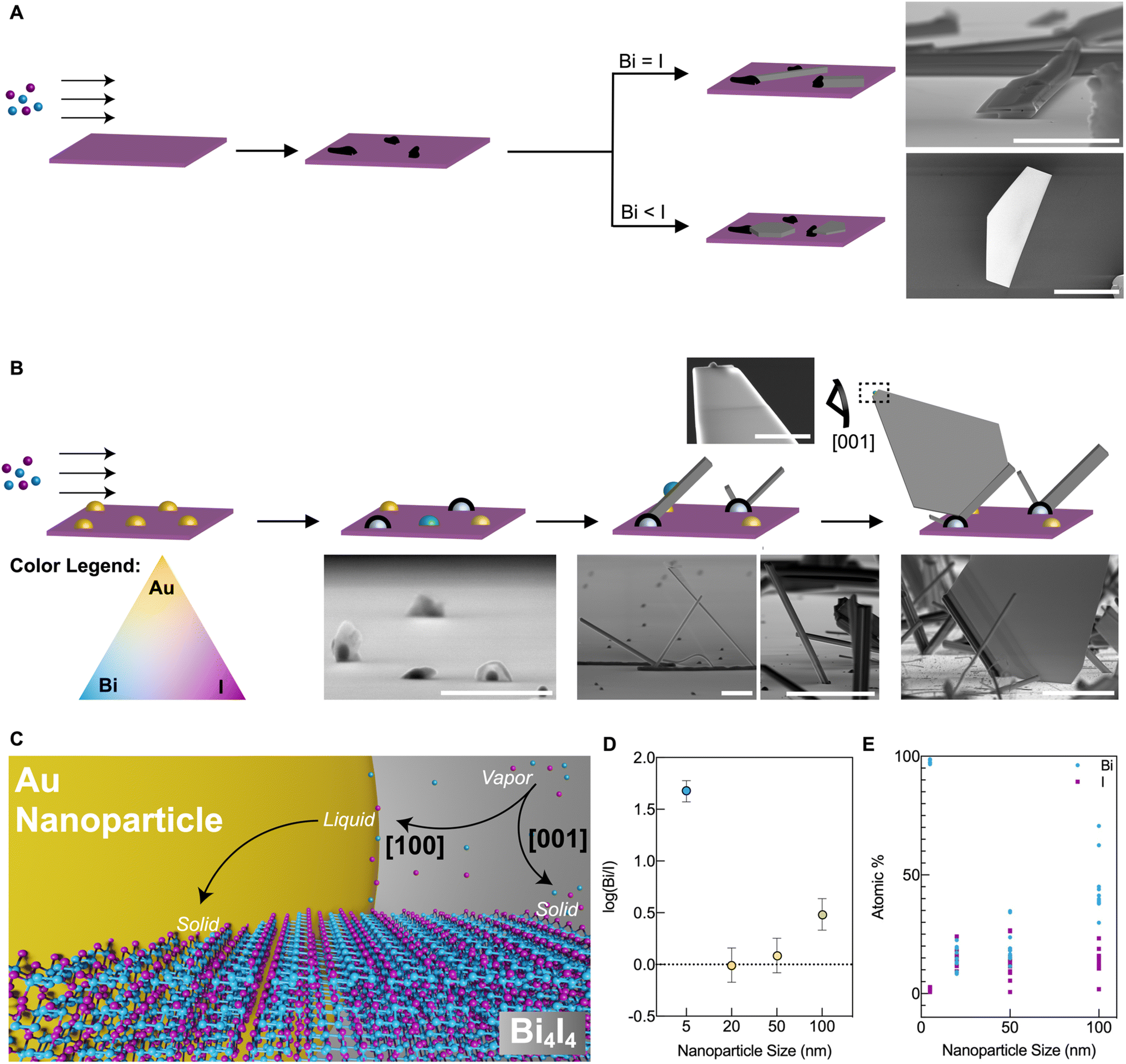 | ||
| Fig. 4 Growth pathways involved in the crystallization of Bi4I4 nanowires and quasi-2D nanosheets. (A) Schematic of the proposed CVD growth reaction pathway of BixIy nanocrystals in the absence of Au NPs. Black regions represent BixIy nucleation spots and gray particles represent the growing nanocrystals. SEM images of Bi4I4 (Bi = I; Scale bar, 5 μm) and BiI3 (Bi < I; scale bar, 50 μm) nanocrystals are included beside the corresponding schematic figure. (B) Schematic of the proposed CVD growth pathway of Bi4I4 nanocrystals with Au NPs present on the growth substrate. A Bi/I/Au color legend for the depicted nanoparticles is added for better visualization. Green nanoparticles highlight Au NPs that are picked up by growing nanowires. SEM images of nanostructures corresponding to each step are shown below the schematic. Scale bars (from left to right): 500 nm, 1 μm, 10 μm, and 10 μm. A high-magnification SEM image of the tip of a flag-like quasi-2D nanosheet is included for reference. Scale bar, 2 μm. (C) Graphical representation of the dashed boxed region in the quasi-2D nanosheet in (B), depicting the VLS growth along the [100] vdW direction and VS growth along the [001] vdW direction. (D) and (E) Dependence of Bi and I dissolution on the diameters of Au NPs presented as Bi-to-I ratios plotted in a logarithm scale (D) and atomic percentages of Bi and I (E). Values shown in (D) and (E) were derived from EDS compositions of on-substrate nanoparticles post-reaction (n = 10 particles per Au NP diameter). | ||
Because the presence of Au NPs significantly altered the crystalline growth of Bi4I4 nanostructures, we looked into the dependence of the nanoscale morphologies on the diameter of Au NPs (Fig. 4B and C). High-resolution SEM imaging and EDS of Au NPs post-reaction show that the deposition of BixIy species from the vapor phase occurs almost exclusively on the Au NPs (Fig. S4†). The post-synthetic compositional information from EDS of Au NPs that did not have any nanostructure growth serves as a semi-quantitative guide to understand the Au-NP-dependency of dimensionalities in Bi4I4 nanostructures.57,58 The resulting Au NP nucleation points showed varying post-synthetic Bi:I:Au compositions, indicating the Au NP diameter-dependent solvation of bismuth and iodine in the Au NPs (Tables S8–S11†). A control reaction with only HgI2 showed that iodine did not dissolve in the Au NPs without the presence of bismuth. The formation of the ternary Bi:I:Au nucleation points requires the presence of Bi (Table S12†).59 While a eutectic mixture of Au and Bi is expected to form at about 240 °C.42 and the maximum calibrated temperature reached on the growth substrates is 238 °C, we still observed Au NPs with solvated Bi and I even at the lower temperature regions of the substrate. This observation is consistent with a size or confinement-induced Bi:Au eutectic formation, which has also been observed for other crystalline systems.42,60
From the results gathered in this study, we found that Bi and I dissolve in the Au NPs until they reach a critical saturation point. Originating from these nucleation points, Bi4I4 nanowires then grow at a protruding angle, sometimes singly, but frequently in large urchin-like radial growth clusters (Fig. 4B). Notably, Au NPs were never observed at the tip of the resulting Bi4I4 nanowires post-reaction. Following nucleation, and with the absence of an Au NP at the nanowire terminus, continued growth of Bi4I4 nanowires is best described by a VS growth pathway.53–56 Beyond the size control afforded by different Au NP diameters, we found that the emergence and density of the nanosheets on the substrate depended on the Au NP diameter. EDS analysis of the resulting Bi:I ratios in the Au NPs on the substrate surface from which no Bi4I4 nanocrystals grew from showed that the dissolution of Bi and I in the Au NPs is generally unequal and often on the Bi-rich side (Fig. 4D and E, Tables S8–S11†). In this scenario, more commonly observed in reactions with 100 nm, 50 nm, and 5 nm diameter Au NPs, the growths produced predominantly Bi4I4 nanowires from a VS pathway. When there are stoichiometrically equivalent Bi and I in the Au NPs (i.e. log(Bi/I) = 0 and %Bi ≅ %I ≅ 15%; Fig. 4D and E), as is the case for Au NPs with 20 nm diameters, we observed the densest growth of quasi-2D Bi4I4 nanosheets. Due to the lower probability that this ideal 1:1 ratio could also be found in Au NPs of different sizes on the growth substrate surface, we infrequently observed quasi-2D nanosheets in syntheses which involved Au NPs with 100 nm and 50 nm diameters. Hereon, we will refer to Au NPs meeting this condition (i.e. log(Bi/I) = 0) as “equistoichiometric” NPs (depicted as green in Fig. 4B).
We posit that the greater proportion of on-substrate 20 nm Au NPs that meet this equistoichiometric condition in comparison to the other size NPs tested in this study is due to a nanoscale size-dependent liquidus shift and a subsequent iodine saturation. It is common knowledge that nanoscale phase diagrams differ from that of the bulk, and this fact has been studied extensively in other VLS systems.58 We have shown in a control reaction that the lower-melting point mixture formed between the Au NPs and the vapor phase precursors requires the presence of Bi (Table S12†). This is suggestive that there is an Au NP size-dependent liquidus, with the amount of Bi required to form the liquid mixture decreasing with the decreasing Au NP diameter. Indeed, the average percent composition of Bi in the Au NPs post reaction is observed to decrease from 45 ± 12% Bi in 100 nm Au NPs to 18 ± 7% Bi in 50 nm Au NPs to 15 ± 7% Bi in 20 nm Au NPs before drastically increasing to 97.7 ± 0.7% Bi in 5 nm Au NPs (Fig. 4E and Tables S8–S11†). Once a liquid nanoparticle is formed from the Bi–Au alloy, I atoms can then saturate the NP as well. The drastic increase in % Bi observed for the 5 nm Au NPs can be attributed to the extreme size effect of the 5 nm Au NPs, where the Au NP fully saturates with bismuth and prevents any iodine from dissolving. Interestingly, post-reaction EDS analysis shows that the percent composition of I does not follow a similar trend to Bi and remains constant at about ∼15% I for all nanoparticle diameters (except for the 5 nm diameter Au NPs) (Fig. 4E and Tables S8–S11†). Because the average percent composition of I is 15% for all sizes of Au NPs, the 20 nm Au NPs represent the catalyst size with the greatest probability of harboring an equistoichiometric ratio of Bi:I (1:1) as the average percent composition of Bi is ∼15% only for the 20 nm Au NPs.
During the VS growth of Bi4I4 nanowires from on-substrate Au NP nucleation points, the growing nanowire incorporates an equistoichiometric Au NP on its surface. Post-synthesis, Au NPs were observed on the surface of Bi4I4 nanowires (Fig. 4B and S13†). The growth of the nanosheet is then catalyzed by an Au NP which is assumed to be lifted off the surface of the nanowire as the nanosheet grows (Fig. 4B). The evidence for this mechanism, and the hallmark of VLS growth,46,61 was the presence of a nanoparticle catalyst observed at the tip of the nanosheets (Fig. 4B and S6†). Further evidence in strong support of this mechanism is that no nanosheets were observed without a nanowire base (Fig. 3H and S4†). There is a proximity effect of the on-substrate equistoichiometric Au NP to the growing Bi4I4 nanowire, wherein, a growing Bi4I4 nanowire incorporates NPs in proximity and directs the crystallization of nanosheets. To support this proposed growth pathway, we prepared a control reaction with a tenfold dilution of the solution used to deposit 20 nm diameter Au NPs on the substrate. With the significantly decreased density of the catalyst, this sparse Au NP coverage on the substrate resulted in widely dispersed growth of Bi4I4 nanowires. No nanosheets were observed under these conditions (Fig. S14†). We also note that the Au NP density on the substrate surface is not the sole variable that determines the density and morphology of CVD-grown Bi4I4 nanostructures. AFM analysis of Au NPs with different diameters dropcasted on SiO2/Si substrates reveals that the densest deposition of Au NPs, which is seen with the 5 nm diameter Au NPs, squarely corresponds with the least dense growth of Bi4I4 nanosheets (Fig. S15 and Table S13†). Altogether, the conditions which involve equistoichiometric Bi:I ratios (as measured from Au NPs on the substrate) in the Au NPs that were eventually embedded onto VS-grown nanowires uniquely directs the growth of quasi-2D nanosheets of Bi4I4.
We rationalize the growth of flag-like triangular Bi4I4 quasi-2D nanosheets based on the presence of Au NPs during the growth, the highly anisotropic bonding, and the crystalline structure and habit of the q-1D vdW Bi4I4 lattice. Au NPs seated on the surface of the nanowires could theoretically catalyze the growth of quasi-2D sheets along the vdW bonding directions perpendicular to the covalent axis. The corresponding (100) and (001) facets normal to these vdW directions both provide a suitable lattice matched surface with the underlying nanowire (Fig. 1A). We, however, found that the only growth direction catalyzed by the Au NPs is along the [100]-direction as confirmed by complementary EBSD (Fig. 3K), HAADF-STEM (Fig. 3L–N), and SAED (Fig. S10†) experiments. Similar to other chalcogen-containing vdW solids, this growth pattern points to the probable role of the coordination geometry of the internal Bi atoms in the [Bi4I4]n chains in promoting the lateral assembly of chains along the [100]-direction. This is corroborated by the anisotropic inter-chain Bi–I distances and the 3-coordinate Bi atoms whose lone pairs are oriented directly at a proximal I atom on an adjacent chain along the a-axis or [100]-direction, suggesting the stereochemically active lone pair promoted growth along this crystallographic direction (ESI; Fig. S16 and S17†). Remarkably, the (001) facet that emerged from the VLS-catalyzed growth of a quasi-2D nanosheet along the [100]-direction is one of the sought-after orientations that could harbor topologically protected hinge states in the low-temperature α-Bi4I4 phase.30,62
Continued growth of quasi-2D nanosheets can be described by both VLS and VS pathways (Fig. 4C). Deposition of BixIy vapor on the Au NPs generally results in faster VLS growth along the [100]-direction, while deposition of BixIy vapor on the other facets of the quasi-2D sheets results in the slower VS growth. The crystallization of quasi-2D nanosheets in the form of a triangular flag-like nanocrystal that are thinner along the [001] direction hints at the preferred growth along the covalent direction (b-axis, [010]-direction) compared to the non-catalyzed vdW direction (c-axis, [001]-direction). These arguments are consistent with earlier observations from EBSD and HAADF-STEM, where the resulting morphology of the quasi-2D nanosheets could be reconstructed by considering the crystalline habit of the monoclinic unit cell of Bi4I4. The triangular morphology of the resulting Bi4I4 quasi-2D nanosheets can be described by a monoclinic crystalline habit with faces bound by (001), (110), and (100) surfaces (Fig. S18†). As the catalyzed growth in the [100]-direction occurs more readily than the other vdW direction ([001]-direction), thin quasi-2D nanosheets were observed to form with their base bound by the (100) facet terminating at the surface of the underlying nanowire. Beyond the structure- and anisotropy-prescribed formation of quasi-2D nanosheets, we also found that higher I content in precursor Bi:I ratio promotes the crystallization of elongated quasi-2D nanosheets (ESI; Fig. 2A under 320 °C and 4:2 Bi-to-I ratio; Table S14†).
Conclusion
In summary, we have demonstrated that the growth of well-defined Bi4I4 nanowires and quasi-2D nanosheets in the presence of Au NPs occurs based on both VS and VLS pathways. The directed growth of dimensionally resolved Bi4I4 nanostructures is modulated by the degree of dissolution of Bi and I in the Au NP catalysts which, in turn, dictate the critical Bi:I ratios during the synthesis. We established that the VLS pathway exclusively results in the formation of quasi-2D nanosheets. VLS growth of Bi4I4 quasi-2D nanosheets occurs when there is an equal amount of Bi and I in the Au NP catalysts on the substrate surface, which we found was highly dependent on the Au NP diameter. The resulting Bi4I4 nanostructures present an ideal foundation to study size-, composition-, and dimensionality-dependent emergent physics arising from the topologically protected and spin-resolved electronic states (surface and edge) in Bi4I4 as well as their interfacing with other low-dimensional vdW materials. Owing to the structural resemblance of the Bi4I4 lattice to other 1D and q-1D vdW crystals, we anticipate that these findings could guide synthetic efforts towards well-defined nanostructures in the presence of a catalyst for a library of 1D and q-1D vdW phases.
Data availability
All data are available in the main text or the ESI.†Author contributions
S. J. A. carried out the experimental work and was supported by D. L. M. C., M. H., and T. A. in the synthesis, AFM characterization, and STEM analyses of the samples. S. J. A. and M. Q. A. prepared the manuscript with contributions from D. L. M. C., M. H., and T. A. on the respective sections that correspond to the experiments that they contributed to. M. Q. A. supervised the project.Conflicts of interest
Authors declare that they have no competing interests.Acknowledgements
S. J. A. and M. Q. A. acknowledge the Eddleman Quantum Institute (EQI) for support through the EQI Graduate Student Fellowship program. We thank the UC Irvine Materials Research Institute (IMRI) for instrumental support in several aspects of this work. Facilities and instrumentation at IMRI are supported, in part, by the National Science Foundation through the UC Irvine Materials Research Science and Engineering Center grant number DMR-2011967. AFM was performed using an Anton Paar Tosca 400 AFM on loan to IMRI from Anton Paar GmbH. We also thank the UC Irvine Laser Spectroscopy Labs and its director, Dr Dmitry Fishman. We also recognize the valuable and insightful discussions with J. D. Sanchez-Yamagishi and L. Jauregui.References
- C.-C. Liu, W. Feng and Y. Yao, Quantum spin Hall effect in silicene and two-dimensional germanium, Phys. Rev. Lett., 2011, 107(7), 076802 CrossRef PubMed.
- F. Schindler, Z. Wang, M. G. Vergniory, A. M. Cook, A. Murani, S. Sengupta, A. Y. Kasumov, R. Deblock, S. Jeon and I. Drozdov, Higher-order topology in bismuth, Nat. Phys., 2018, 14(9), 918–924 Search PubMed.
- L. Kou, Y. Ma, Z. Sun, T. Heine and C. Chen, Two-dimensional topological insulators: progress and prospects, J. Phys. Chem. Lett., 2017, 8(8), 1905–1919 Search PubMed.
- J. M. Park, Y. Cao, K. Watanabe, T. Taniguchi and P. Jarillo-Herrero, Tunable strongly coupled superconductivity in magic-angle twisted trilayer graphene, Nature, 2021, 590(7845), 249–255 CrossRef CAS PubMed.
- J. R. Schaibley, H. Yu, G. Clark, P. Rivera, J. S. Ross, K. L. Seyler, W. Yao and X. Xu, Valleytronics in 2D materials, Nat. Rev. Mater., 2016, 1(11), 1–15 Search PubMed.
- H. Li, S. Li, E. C. Regan, D. Wang, W. Zhao, S. Kahn, K. Yumigeta, M. Blei, T. Taniguchi and K. Watanabe, Imaging two-dimensional generalized Wigner crystals, Nature, 2021, 597(7878), 650–654 CrossRef CAS PubMed.
- B. He, Y. Wang, M. Q. Arguilla, N. D. Cultrara, M. R. Scudder, J. E. Goldberger, W. Windl and J. P. Heremans, The Fermi surface geometrical origin of axis-dependent conduction polarity in layered materials, Nat. Mater., 2019, 18(6), 568–572 CrossRef CAS PubMed.
- L. Li, J. Kim, C. Jin, G. J. Ye, D. Y. Qiu, F. H. Da Jornada, Z. Shi, L. Chen, Z. Zhang and F. Yang, Direct observation of the layer-dependent electronic structure in phosphorene, Nat. Nanotechnol., 2017, 12(1), 21–25 CrossRef CAS PubMed.
- M. C. Watts, L. Picco, F. S. Russell-Pavier, P. L. Cullen, T. S. Miller, S. P. Bartuś, O. D. Payton, N. T. Skipper, V. Tileli and C. A. Howard, Production of phosphorene nanoribbons, Nature, 2019, 568(7751), 216–220 CrossRef CAS PubMed.
- S. Wang, Y. Rong, Y. Fan, M. Pacios, H. Bhaskaran, K. He and J. H. Warner, Shape evolution of monolayer MoS2 crystals grown by chemical vapor deposition, Chem. Mater., 2014, 26(22), 6371–6379 CrossRef CAS.
- T. Chowdhury, J. Kim, E. C. Sadler, C. Li, S. W. Lee, K. Jo, W. Xu, D. H. Gracias, N. V. Drichko and D. Jariwala, Substrate-directed synthesis of MoS2 nanocrystals with tunable dimensionality and optical properties, Nat. Nanotechnol., 2020, 15(1), 29–34 CrossRef CAS PubMed.
- S. Li, Y.-C. Lin, W. Zhao, J. Wu, Z. Wang, Z. Hu, Y. Shen, D.-M. Tang, J. Wang and Q. Zhang, Vapour–liquid–solid growth of monolayer MoS2 nanoribbons, Nat. Mater., 2018, 17(6), 535–542 CrossRef CAS PubMed.
- P. Sutter, S. Wimer and E. Sutter, Chiral twisted van der Waals nanowires, Nature, 2019, 570(7761), 354–357 CrossRef CAS PubMed.
- Y. Liu, J. Wang, S. Kim, H. Sun, F. Yang, Z. Fang, N. Tamura, R. Zhang, X. Song and J. Wen, Helical van der Waals crystals with discretized Eshelby twist, Nature, 2019, 570(7761), 358–362 CrossRef CAS PubMed.
- A. Aljarb, J.-H. Fu, C.-C. Hsu, C.-P. Chuu, Y. Wan, M. Hakami, D. R. Naphade, E. Yengel, C.-J. Lee and S. Brems, Ledge-directed epitaxy of continuously self-aligned single-crystalline nanoribbons of transition metal dichalcogenides, Nat. Mater., 2020, 19(12), 1300–1306 CrossRef CAS PubMed.
- R. Xiang, T. Inoue, Y. Zheng, A. Kumamoto, Y. Qian, Y. Sato, M. Liu, D. Tang, D. Gokhale and J. Guo, One-dimensional van der Waals heterostructures, Science, 2020, 367(6477), 537–542 CrossRef CAS PubMed.
- A. A. Balandin, F. Kargar, T. T. Salguero and R. K. Lake, One-dimensional van der Waals quantum materials, Mater. Today, 2022, 55, 74–91 CrossRef.
- Y. Qu, M. Q. Arguilla, Q. Zhang, X. He and M. Dincă, Ultrathin, high-aspect ratio, and free-standing magnetic nanowires by exfoliation of ferromagnetic quasi-one-dimensional van der Waals lattices, J. Am. Chem. Soc., 2021, 143(46), 19551–19558 CrossRef CAS PubMed.
- F. Kargar, Z. Barani, N. R. Sesing, T. T. Mai, T. Debnath, H. Zhang, Y. Liu, Y. Zhu, S. Ghosh and A. J. Biacchi, Elemental excitations in MoI3 one-dimensional van der Waals nanowires, Appl. Phys. Lett., 2022, 121(22), 221901 CrossRef CAS.
- G. Liu, S. Rumyantsev, M. A. Bloodgood, T. T. Salguero, M. Shur and A. A. Balandin, Low-frequency electronic noise in quasi-1D TaSe3 van der Waals nanowires, Nano Lett., 2017, 17(1), 377–383 CrossRef CAS PubMed.
- N. Shumiya, M. S. Hossain, J.-X. Yin, Z. Wang, M. Litskevich, C. Yoon, Y. Li, Y. Yang, Y.-X. Jiang and G. Cheng, Evidence of a room-temperature quantum spin Hall edge state in a higher-order topological insulator, Nat. Mater., 2022, 21(10), 1111–1115 CrossRef CAS PubMed.
- D. Pfister, K. Schäfer, C. Ott, B. Gerke, R. Pöttgen, O. Janka, M. Baumgartner, A. Efimova, A. Hohmann and P. Schmidt, Inorganic double helices in semiconducting SnIP, Adv. Mater., 2016, 28(44), 9783–9791 CrossRef CAS PubMed.
- Y. Zhu, D. A. Rehn, E. R. Antoniuk, G. Cheon, R. Freitas, A. Krishnapriyan and E. J. Reed, Spectrum of exfoliable 1D van der Waals molecular wires and their electronic properties, ACS Nano, 2021, 15(6), 9851–9859 CrossRef CAS PubMed.
- N. Dhar, N. Syed, M. Mohiuddin, A. Jannat, A. Zavabeti, B. Y. Zhang, R. S. Datta, P. Atkin, N. Mahmood and D. Esrafilzadeh, Exfoliation behavior of van der Waals strings: case study of Bi2S3, ACS Appl. Mater. Interfaces, 2018, 10(49), 42603–42611 CrossRef CAS PubMed.
- A. Geremew, M. Bloodgood, E. Aytan, B. Woo, S. Corber, G. Liu, K. Bozhilov, T. Salguero, S. Rumyantsev and M. Rao, Current carrying capacity of quasi-1D ZrTe3 van der Waals nanoribbons, IEEE Electron Device Lett., 2018, 39(5), 735–738 CAS.
- E. Baldini, A. Zong, D. Choi, C. Lee, M. H. Michael, L. Windgaetter, I. I. Mazin, S. Latini, D. Azoury and B. Lv, The spontaneous symmetry breaking in Ta2NiSe5 is structural in nature, Proc. Natl. Acad. Sci. U. S. A., 2023, 120(17), e2221688120 CrossRef CAS PubMed.
- M. Sotome, M. Nakamura, J. Fujioka, M. Ogino, Y. Kaneko, T. Morimoto, Y. Zhang, M. Kawasaki, N. Nagaosa and Y. Tokura, Spectral dynamics of shift current in ferroelectric semiconductor SbSI, Proc. Natl. Acad. Sci. U. S. A., 2019, 116(6), 1929–1933 CrossRef CAS PubMed.
- D. L. M. Cordova, K. Chua, R. M. Huynh, T. Aoki and M. Q. Arguilla, Anisotropy-Driven Crystallization of Dimensionally Resolved Quasi-1D Van der Waals Nanostructures, J. Am. Chem. Soc., 2023, 145(41), 22413–22424 CrossRef CAS PubMed.
- H. Okamoto and H. Okamoto, Phase diagrams for binary alloys, ASM international Materials Park, OH, 2000 Search PubMed.
- J. Huang, S. Li, C. Yoon, J. S. Oh, H. Wu, X. Liu, N. Dhale, Y.-F. Zhou, Y. Guo and Y. Zhang, Room-temperature topological phase transition in quasi-one-dimensional material Bi4I4, Phys. Rev. X, 2021, 11(3), 031042 CAS.
- Y. Liu, R. Chen, Z. Zhang, M. Bockrath, C. N. Lau, Y.-F. Zhou, C. Yoon, S. Li, X. Liu and N. Dhale, Gate-tunable transport in quasi-one-dimensional α-Bi4I4 field effect transistors, Nano Lett., 2022, 22(3), 1151–1158 CrossRef CAS PubMed.
- G. Autès, A. Isaeva, L. Moreschini, J. C. Johannsen, A. Pisoni, R. Mori, W. Zhang, T. G. Filatova, A. N. Kuznetsov and L. Forró, A novel quasi-one-dimensional topological insulator in bismuth iodide β-Bi4I4, Nat. Mater., 2016, 15(2), 154–158 CrossRef PubMed.
- P. Wang, F. Tang, P. Wang, H. Zhu, C.-W. Cho, J. Wang, X. Du, Y. Shao and L. Zhang, Quantum transport properties of β-Bi4I4 near and well beyond the extreme quantum limit, Phys. Rev. B, 2021, 103(15), 155201 CrossRef CAS.
- J. Han, W. Xiao and Y. Yao, Quasi-one-dimensional topological material Bi4X4 (X=Br,I), Adv. Phys.: X, 2022, 7(1), 2057234 Search PubMed.
- C.-C. Liu, J.-J. Zhou, Y. Yao and F. Zhang, Weak topological insulators and composite Weyl semimetals: β−Bi4X4 (X = Br, I), Phys. Rev. Lett., 2016, 116(6), 066801 CrossRef PubMed.
- X. Li, D. Chen, M. Jin, D. Ma, Y. Ge, J. Sun, W. Guo, H. Sun, J. Han and W. Xiao, Pressure-induced phase transitions and superconductivity in a quasi–1-dimensional topological crystalline insulator α-Bi4Br4, Proc. Natl. Acad. Sci. U. S. A., 2019, 116(36), 17696–17700 CrossRef CAS PubMed.
- H. G. von Schnering, H. von Benda and C. Kalveram, Wismutmonojodid BiJ, eine Verbindung mit Bi (0) und Bi (II), Z. Anorg. Allg. Chem., 1978, 438(1), 37–52 CrossRef CAS.
- D. Tiwari, D. Alibhai and D. J. Fermin, Above 600 mV open-circuit voltage BiI3 solar cells, ACS Energy Lett., 2018, 3(8), 1882–1886 CrossRef CAS.
- X. Wang, J. Wu, J. Wang, T. Chen, H. Gao, P. Lu, Q. Chen, C. Ding, J. Wen and J. Sun, Pressure-induced structural and electronic transitions in bismuth iodide, Phys. Rev. B, 2018, 98(17), 174112 CrossRef CAS.
- M. Hapase, V. Tare and A. Biswas, Oxidation of bismuth, Acta Metall., 1967, 15(1), 131–133 CrossRef CAS.
- R. E. Brandt, R. C. Kurchin, R. L. Hoye, J. R. Poindexter, M. W. Wilson, S. Sulekar, F. Lenahan, P. X. Yen, V. Stevanovic and J. C. Nino, Investigation of bismuth triiodide (BiI3) for photovoltaic applications, J. Phys. Chem. Lett., 2015, 6(21), 4297–4302 CrossRef CAS PubMed.
- H. Okamoto and T. Massalski, The Au−Bi (gold-bismuth) system, Bull. Alloy Phase Diagrams, 1983, 4, 401–407 CrossRef.
- S. N. Mohammad, Analysis of the vapor–liquid–solid mechanism for nanowire growth and a model for this mechanism, Nano Lett., 2008, 8(5), 1532–1538 CrossRef CAS PubMed.
- R. A. Puglisi, C. Bongiorno, S. Caccamo, E. Fazio, G. Mannino, F. Neri, S. Scalese, D. Spucches and A. La Magna, Chemical vapor deposition growth of silicon nanowires with diameter smaller than 5 nm, ACS Omega, 2019, 4(19), 17967–17971 CrossRef CAS PubMed.
- Y. Wu and P. Yang, Direct observation of vapor−liquid−solid nanowire growth, J. Am. Chem. Soc., 2001, 123(13), 3165–3166 CrossRef CAS.
- R. S. Wagner and W. C. Ellis, Vapor-liquid-solid mechanism of single crystal growth, Appl. Phys. Lett., 1964, 4(5), 89–90 CrossRef CAS.
- E. Sutter, J. S. French and P. Sutter, Tunable layer orientation and morphology in vapor–liquid–solid growth of one-dimensional GeS van der Waals nanostructures, Chem. Mater., 2021, 33(11), 3980–3988 CrossRef CAS.
- J. S. Lee, S. Brittman, D. Yu and H. Park, Vapor–liquid–solid and vapor–solid growth of phase-change Sb2Te3 nanowires and Sb2Te3/GeTe nanowire heterostructures, J. Am. Chem. Soc., 2008, 130(19), 6252–6258 CrossRef CAS PubMed.
- S. S. Hong, Y. Zhang, J. J. Cha, X.-L. Qi and Y. Cui, One-dimensional helical transport in topological insulator nanowire interferometers, Nano Lett., 2014, 14(5), 2815–2821 CrossRef CAS PubMed.
- D. Kong, J. C. Randel, H. Peng, J. J. Cha, S. Meister, K. Lai, Y. Chen, Z.-X. Shen, H. C. Manoharan and Y. Cui, Topological insulator nanowires and nanoribbons, Nano Lett., 2010, 10(1), 329–333 CrossRef CAS PubMed.
- M. Saghir, M. R. Lees, S. J. York and G. Balakrishnan, Synthesis and characterization of nanomaterials of the topological crystalline insulator SnTe, Cryst. Growth Des., 2014, 14(4), 2009–2013 CrossRef CAS.
- Y. Yang, C. Wang, J. Hou and J. Dai, Raman scattering, far infrared spectrum of BiI3 nanocrystallites, Mater. Lett., 2003, 57(15), 2185–2188 CrossRef CAS.
- A. Umar, S. Kim, Y.-S. Lee, K. Nahm and Y. Hahn, Catalyst-free large-quantity synthesis of ZnO nanorods by a vapor–solid growth mechanism: structural and optical properties, J. Cryst. Growth, 2005, 282(1–2), 131–136 CrossRef CAS.
- S. Ambrosini, M. Fanetti, V. Grillo, A. Franciosi and S. Rubini, Vapor-liquid-solid and vapor-solid growth of self-catalyzed GaAs nanowires, AIP Adv., 2011, 1(4), 042142 CrossRef.
- S. Wu, C. Huang, G. Aivazian, J. S. Ross, D. H. Cobden and X. Xu, Vapor–solid growth of high optical quality MoS2 monolayers with near-unity valley polarization, ACS Nano, 2013, 7(3), 2768–2772 CrossRef CAS PubMed.
- G. Shen, D. Chen, P.-C. Chen and C. Zhou, Vapor−solid growth of one-dimensional layer-structured gallium sulfide nanostructures, ACS Nano, 2009, 3(5), 1115–1120 CrossRef CAS PubMed.
- H. Lu and X. Meng, Nanophase diagram of binary eutectic Au-Ge nanoalloys for vapor-liquid-solid semiconductor nanowires growth, Sci. Rep., 2015, 5(1), 11263 CrossRef PubMed.
- E. Sutter and P. Sutter, Phase diagram of nanoscale alloy particles used for vapor−liquid−solid growth of semiconductor nanowires, Nano Lett., 2008, 8(2), 411–414 CrossRef CAS PubMed.
- E. D. Leshchenko, M. Ghasemi, V. G. Dubrovskii and J. Johansson, Nucleation-limited composition of ternary III–V nanowires forming from quaternary gold based liquid alloys, CrystEngComm, 2018, 20(12), 1649–1655 RSC.
- S. Kodambaka, J. Tersoff, M. Reuter and F. Ross, Germanium nanowire growth below the eutectic temperature, Science, 2007, 316(5825), 729–732 CrossRef CAS PubMed.
- K. A. Dick, K. Deppert, M. W. Larsson, T. Mårtensson, W. Seifert, L. R. Wallenberg and L. Samuelson, Synthesis of branched 'nanotrees' by controlled seeding of multiple branching events, Nat. Mater., 2004, 3(6), 380–384 CrossRef CAS PubMed.
- C. Yoon, C.-C. Liu, H. Min and F. Zhang, Quasi-one-dimensional higher-order topological insulators, arXiv, 2020, preprint, arXiv:2005.14710, DOI:10.48550/arXiv.2005.14710.
Footnote |
| † Electronic supplementary information (ESI) available. See DOI: https://doi.org/10.1039/d3sc06456e |
| This journal is © The Royal Society of Chemistry 2024 |