
 Open Access Article
 This Open Access Article is licensed under a Creative Commons Attribution-Non Commercial 3.0 Unported Licence
Carrier behavior of a carbon material assisted TIPS-pentacene composite film for improvement of electrical conductivity
Moonjeong Boka,
Ju Ho Leeab,
Kanghee Won *c and
Eunju Lim*a
*c and
Eunju Lim*a
aDepartment of Science Education/Convergent Systems Engineering, Dankook University, Gyeonggi-do, Republic of Korea. E-mail: elim@dankook.ac.kr
bDepartment of Engineering, Dankook University, Gyeonggi-do, Republic of Korea
cDepartment of Information Display, College of Science, Kyung Hee University, 26 Kyungheedae-ro, Dongdaemun-gu, Seoul, 02447, Republic of Korea. E-mail: khwon@khu.ac.kr
First published on 13th November 2024
Abstract
Organic semiconductor devices have a lower intrinsic carrier density than inorganic semiconductors, and improving their electrical conductivity is important for organic electronic devices. Further theoretical investigations and understanding the properties of these electronic devices are necessary to improve the electrical conductivity of organic devices. In this study, we demonstrate how two carbon-material-assisted organic semiconductor devices affect the electrical conductivity and charge mechanism by using electrical measurements (i.e., I–V and C–V measurements, and numerical simulations). To clearly demonstrate the enhancement of the charge injection into TIPS (6,13-bis(triisopropylsilylethynyl)-pentacene), we studied the blending effect of carbon materials (carbon nanotube and fullerene) in TIPS and discussed injection, transport and charge accumulation of hole and electron in relation to trapped charge. This study will be helpful for understanding charge mechanisms in composite organic semiconductor devices.
1. Introduction
The development of organic electronic devices, which have a variety of potential applications including displays, solar cells, and sensors, has been rapid over the past few decades. However, further improvements are required to meet the expectations of the modern electronics industry.1–6 In comparison to Si-based semiconductor devices, organic semiconductor devices exhibit a lower intrinsic carrier density, and low carrier injection characteristics can diminish the efficiency of the device.7–9 Furthermore, organic semiconductor films manufactured using the solution spin casting method have low charge carrier mobility because charge transport in disordered structures due to solvent evaporation or speed conditions can be limited by the hopping process between polymer chains in the disordered regions.10–14 Therefore, the conductivity of organic semiconductor devices is attributed to the materials employed and the manufacturing conditions. A variety of structural and material approaches, incorporating a range of metals and/or semiconductor materials, has been employed to control the electrical conductivity and assist in the charge transport process.15,16 In general, improvements in the conductivity of organic semiconductors (i.e., improving carrier injection) can be achieved by blending components or by chemical doping of bulk organic semiconductors.For example, carbon nanotubes (CNTs), which are known as conductive fillers, have been incorporated into semiconductor materials or electrodes due to their high aspect ratio, excellent conductivity, mechanical flexibility, and solution-processing compatibility.17–20 A heterogeneously dispersed aggregation of CNTs within the polymer can limit device performance.21–23 Therefore, well-dispersed materials in polymers can be improved to match the existing electrical conductivity properties of organic semiconductor materials, and the carrier mechanism analysis of carrier injection, transport, and accumulation phenomena has a great potential for other types of electronic devices and semiconductor classes.24
Herein, we report the electrical characteristics of conductive carbon materials assisted by organic semiconductors using heterogeneous blends in terms of carrier injection and accumulation mechanisms. CNTs and fullerenes (C60) are composite materials that are used as fillers. CNTs have a fibrous structure, whereas C60 has a cage-like fused ring structure.25 These carbon isomers play a major role in improving charge injection, transport, and accumulation. C60 is a spherical molecule that is highly soluble due to its dispersibility. Furthermore, it exhibits a high electron affinity as an electron acceptor, rendering it a crucial material for use in organic solar cells and organic light-emitting diodes (OLEDs). The dispersion and structure of carbon materials significantly affect the formation of percolation networks in the composite film.26,27 Carbon composite materials exhibit such charge doping properties in organic devices, and we could analyze the charge behaviors of the active layer in a double-layer diode and a field-effect transistor (FET) structure. The electrical conductivity in organic semiconductor devices is dictated by the chemical structure and concentration of the carbon composites, thereby affecting charge injection and charge trapping. The findings of this study will be of significant help in understanding the charge mechanism in high-performance organic semiconductor devices.
2. Experimental details
2.1 Experimental methods
A CNT (or C60) suspension was prepared using 1,2 dichlorobenzene (ODCB) solution for a stable dispersion, and the TIPS powder was dissolved in a CNT (or C60) suspension at 20 mg/1 mL. The concentration was 0.01, 0.05, and 0.1 wt% relative to TIPS.28,29 The device was manufactured using the same method as in the previous experiment.26,30 The devices consist of organic double-layer diodes with an indium tin oxide (ITO)/polyimide (PI)/TIPS carbon composite/Au structure and organic thin-film transistor (TFT) with an N++Si/SiO2/TIPS carbon composite/Au structure. The electrode area of the diode was 3 mm2, and the channel length and width of the TFT were 40 and 1000 μm, respectively.
2.1.2.1 Electrical measurements. Electrical measurements were conducted using a custom-made vacuum probe station in dark conditions. The I–V curves were plotted using an HP 4155a semiconductor parameter analyzer and controlled using the LabVIEW program. The measurement was done in the direction of +20 V to −20 V (forward scan) and of −20 V to +20 V (backward scan), and the hold time and delay time were both set to 0.1 V s−1. The C–V characteristics were measured using an HP 4192 impedance analyzer with an oscilloscope level of 100 mV.
2.1.2.2 Electrical numerical simulation. To analyze the current density and space charge density effects of carbon-material-assisted organic semiconductor devices, numerical simulation was performed to analyze the effect of increased electrical conductivity in the device, employing the AC/DC module of COMSOL Multiphysics under steady state conditions. The directionality of the organic film was not considered in these simulations.
3. Results and discussions
The conductivity of the organic semiconductor layer is attributed to the properties of the material, directly affecting the carrier injection and transport in organic devices. Blending organic molecules to adjust the electrical conductivity can cause dramatic changes in the electrical conductivity because of various factors, such as the internal structure, weight fraction, and geometry.26,27,31,32Fig. 1 shows the I–V characteristics of the organic double-layered diode as a function of the concentration of carbon materials, CNTs or C60, to increase the electrical conductivity of the TIPS thin film. CNTs and C60 were employed to examine the effect of the suspension dispersion on the charge behavior. Comparisons were made with varying concentrations to analyze the charge behavior within the percolation threshold range of the carbon materials, CNTs and C60 within the TIPS film.
 | ||
| Fig. 1 I–V characteristics of (a) TIPS, (b) TIPS/CNT composite, and (c) TIPS/C60 composite diodes with a concentration of 0.01, 0.05, and 0.1 wt%, respectively. The inset images indicate the schematic representation of each device and enlarged image. | ||
In Fig. 1(a), the TIPS diode has a typical p-type property, and the current value is −1.2 μA in the voltage = −20 V. In contrast, TIPS/carbon composite (CNTs, C60) diodes show similar symmetrical I–V behavior with 0.1 wt% CNTs and C60 in the TIPS material, as shown in Fig. 1(b and c). These show enhanced charge injection of both holes and electrons in the diode, which means ambipolar characteristics. Notably, the increase in electron injection can be estimated as an increase in the conductivity of the TIPS film because of the carbon composite material, which can be roughly calculated from the I–V characteristics.33,34 In steady state, the current across the organic double-layer diode is given by eqn (1), where G1 is the conductance of TIPS and G2 is the conductance of PI.
| I = [(G1G2)/(G1 + G2)]V | (1) |
Therefore, it was possible to evaluate the electric field of the accumulated TIPS film at the interface. The PI layer, which is an insulating layer, causes most of the potential to decrease across the bilayer. The current is given by
| I ≅ G2V, G1 → ∞ | (2) |
Based on the I–V results, in the case of the TIPS device, G2 was estimated as 65 × 10−6 mS using eqn (2), and G1 was estimated to be infinite. Using the calculated G2 in the hole-charging process, G1 is estimated as 4.83 × 10⁻⁶ mS (1). When G1 for each of the carbon materials composite is calculated as above, it is estimated that G1 = 2.19 × 10⁻⁶ S in the case of CNTs and G1 = 2.48 × 10⁻⁶ S in the case of C60. The conductivity of the TIPS changed due to the inserted carbon materials, which supports the shift in the threshold voltage (Vth). In addition, this result suggests that carbon materials can serve as interconnection pathways for the holes and electrons in the TIPS crystalline domains.
Fig. 2(a) shows the optical absorption spectra obtained from the TIPS/carbon composite films using ultraviolet (UV)-visible absorption spectroscopy to analyze the change in the highest occupied molecular orbital (HOMO) and lowest unoccupied molecular orbital (LUMO) energy levels. Therefore, the UV-visible absorption spectrum roughly matches the energy diagram of TIPS, as shown in Fig. 2(b). Each film was prepared using glass/PTS treatment. TIPS film exhibits three peaks at 590, 644, and 698 nm, which are related on the π–π* intraband transition.35
 | ||
| Fig. 2 (a) UV-vis absorption spectra of TIPS/carbon composite films; (b) energy level diagram of Au, MWCNT, TIPS-pentacene and C60. | ||
In the case of the TIPS/carbon composite film, the peaks were slightly blue-shifted compared with those of the as-deposited TIPS film, but the HOMO–LUMO energy band did not change significantly, as shown in the UV-visible absorption spectra. This result suggests that the carbon materials reduce the intermolecular spacing of the TIPS film, causing close contact with the molecular pathway. The strong close-contact polymer chains can be estimated to maximize the charge transfer of the holes and electrons.
Numerical simulations were performed using the AC/DC module of COMSOL Multiphysics under steady-state conditions to visualize the performance of organic devices with improved electrical conductivity, as shown in Fig. 3.
 | ||
| Fig. 3 Numerical simulation using AC/DC module evaluated from (a) potential difference, (b) current density, and (c) space charge density. (i) General organic diode and (ii) organic diode with improved electrical conductivity. | ||
In Fig. 3, (i) represents a generalized organic diode and (ii) represents an organic diode with improved electrical conductivity. In experimental conditions, it can be thought of as TIPS/CNT(C60) with increased conductivity due to CNT(C60). For the potential difference, the organic semiconductor layer in the generalized diode also shows a potential drop similar to that of the insulator, while the improved organic diode shows a potential relatively similar to that of the metal. In addition, Fig. 3(b) shows the enhanced current density inside the organic diode with improved electrical conductivity. Fig. 3(c) illustrates the space-charge density and accumulated charge at the insulator/semiconductor interface inside an organic diode with improved electrical conductivity. Thus, it can be seen that the modification of the organic semiconductor layer can improve electrical conductivity and enhance carrier injection and accumulation inside the device.
In a device with a material property change conductivity (σ = enμ), where σ is the conductivity, μ is the charge mobility, and en is the amount of charge, we observed the I–V characteristic curves and discussed J = enμE.
Since both the charge mobility and the amount of charge are affected by the I–V curve, they must be separated to investigate the effect of doping on charge transport in detail. Therefore, quasi-static capacitance–voltage (C–V) measurements were performed to investigate the carrier accumulation and hysteresis effect in organic devices, as shown in Fig. 4. In Fig. 4(a), the pristine TIPS diode shows typical C–V characteristics with a metal–insulator–semiconductor structure. This indicates that the capacitance increases when a negative bias is applied, indicating hole injection/accumulation at the PI/TIPS interface. Forward and backward scans were performed to compare the capacitance and hysteresis achieved with each carbon dopant. In general, the trapped carriers could be explained through the hysteresis loop, that is, threshold voltage shift (ΔVth).36 It could be related with such as charge traps in gate dielectric and interface trap states between active layer and dielectric.37
 | ||
| Fig. 4 C–V characteristics for (a) TIPS, (b) TIPS/CNT composite, and (c) TIPS/C60 composite diodes with a concentration of 0.01, 0.05, and 0.1 wt%, respectively. | ||
As shown in Fig. 4(b and c), ΔVth increases with increasing concentration of carbon material dopants. Compared to TIPS device, the hysteresis of the TIPS/carbon composite device is strongly dependent on the concentration of carbon materials from 0.01 to 0.1 wt%. Therefore, the ΔVth of the C–V curve to elucidate the trapping effect by embedded carbon materials. In the TIPS/carbon composite device, ΔVth increases from 5 V to 9 V.
In the case of CNTs, from 10 V to 11 V in the case of C60 [see Fig. 5(a)]. This indicates that the majority of the holes are trapped in the carbon materials (CNTs or C60) and/or at the interface of the PI/TIPS carbon composite upon increasing the concentration of carbon materials. The hysteresis of TIPS/C60 was greater than that of TIPS CNT. The difference in the chemical properties of the carbon material composites and hole carriers injected by C60 could result in more trapping at the interface. In addition, there was a slight shift in the TIPS device upon operation, indicating the influence of the interface traps of PI/TIPS. In other words, the hysteresis strongly depends on the embedded carbon materials. The enhanced hysteresis in the C–V curve can be attributed to the reversible storage of holes or electrons in the TIPS/carbon composites and/or defect states at the composite/PI interface [see Fig. 5(b)]. In addition, the capacitance increases as the carbon content increases, indicating an increase in charge accumulation and injection carriers. Therefore, these results support the numerical simulation for improving electrical conductivity. This analysis demonstrates the importance of considering the carrier trapping effect in doping strategies based on nanomaterials. The carrier behavior through hysteresis properties must be considered for effective doping because the proper choice of materials is crucial.
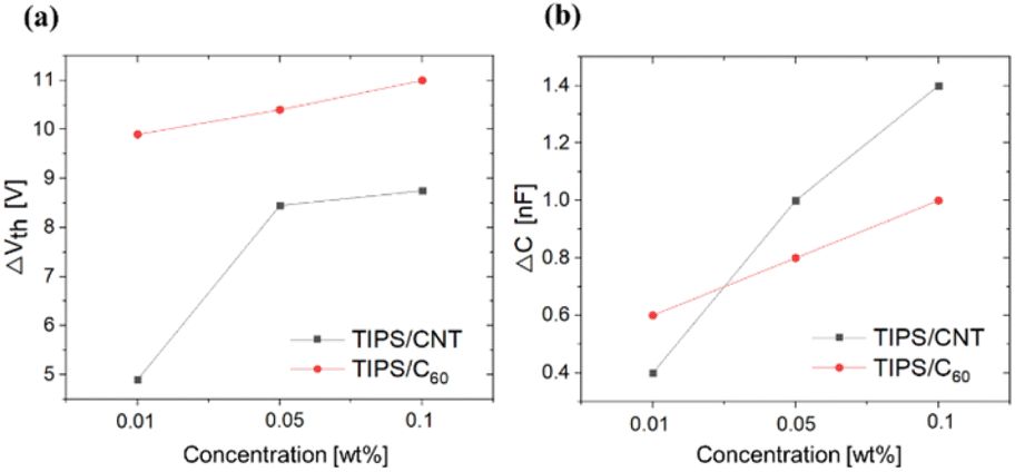 | ||
| Fig. 5 (a) ΔVth and (b) ΔC with the function of the concentration TIPS/CNT and TIPS/C60 double layer diode. | ||
I–V measurements were performed to observe the horizontal transport characteristics after carrier injection from the electrode into the TIPS/carbon composite film using an organic FET structure, as shown in Fig. 6. Fig. 6(a) shows the transfer characteristics at a concentration of 0.1 wt%. The sweep direction to Vgs is from +20 V to −20 V, and Vds is fixed to −20 V. The flowing current of the TIPS/carbon composite was one order of magnitude higher than that of the TIPS, and the order of magnitude of the current was similar to that of the diode.
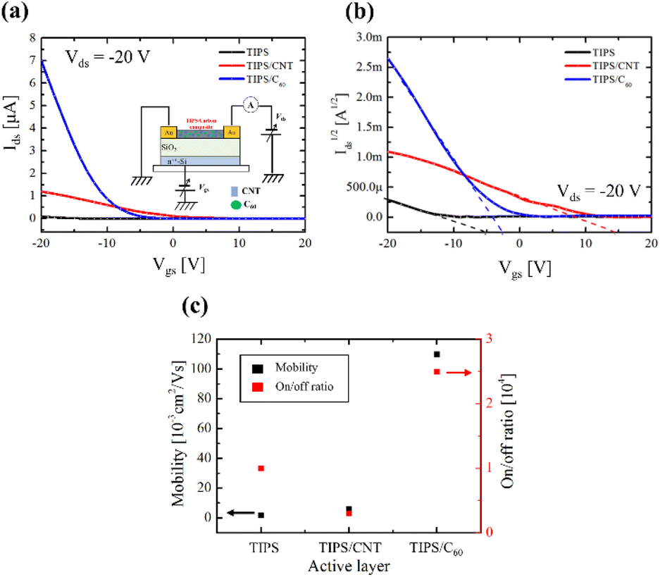 | ||
| Fig. 6 (a) Ids–Vgs characteristics for TIPS/carbon composite FET with the concentration of 0.1 wt%. (b) Replots for √Ids–Vgs and (c) comparison of performance parameter in TIPS/carbon materials composite. The inset image indicates the schematic representation of TIPS/carbon composite FET structure. | ||
Fig. 6(b) shows the √Ids–Vgs plots of TIPS/carbon composite FETs. The p-type threshold voltage of the TIPS FETs showed a significant positive shift with the embedded carbon materials, indicating a change in carrier injection. We could deduce the extracted field effect mobility (μFE) and on/off ratio of TIPS/carbon composite FET, as shown in Fig. 6(c).
The extracted μFE follows the conventional organic FET method.38 The TIPS FET, TIPS/CNTs, and TIPS/C60 FETs have an μFE of 0.1 × 10⁻³, 7 × 10⁻³, and 110 × 10−3 cm2 V−1 s−1, respectively. The carbon materials enhanced the μFE. Notably, the μFE of TIPS/C60 is 100 times higher than that of TIPS/CNT due to its chemical structure and chemical stability. In other words, the embedded carbon materials lowered the electron injection barrier; however, charge trapping occurred at the PI/TIPS/carbon composite interface.
In future studies, it is essential to incorporate time-resolved electric field induced optical second harmonic generation measurements32,33,36 to characterize and specifically discuss carrier trapping and mobility in composite film. This approach will allow for a clearer analysis of the carrier transport mechanism. Also, our research suggests potential applicability in areas where low power consumption is crucial or high-sensitivity measurements are required, such as biosensors for precise detection of biological signals, gas sensors for monitoring specific gas concentrations in the atmosphere, and photodetectors for measuring light intensity.
4. Conclusion
In summary, two different carbon nanocomposite (CNTs and C60) films for high-performance organic semiconductors were fabricated using a heterogeneous blending method. This approach influenced the formation of percolating networks in the composite films. The packing of the composite films was also compared using UV-visible absorption spectral measurements. The results indicate that the spacing between the intermolecular molecules of the TIPS film was reduced because of the carbon materials. This is related to the charge-transfer path in the organic devices. Furthermore, organic diodes and organic TFTs were employed to better evaluate the charge behavior. Devices with a concentration of embedded carbon materials within the percolation thresholds exhibit enhanced charge injection and trapping at the carbon materials CNT, C60, and/or the interface of the PI/TIPS composite. The electrical conductivity and trapping of TIPS/C60 were higher than those of TIPS/CNTs. Thus, we demonstrated that the dispersion and structure of the embedded material is involved in the injection and transport of charge and is dominant in determining the electrical properties of the organic semiconductor device.Data availability
The authors confirm that the data used to support the findings of this study are included within the article and are available from the corresponding author upon reasonable request.Conflicts of interest
There are no conflicts to declare.Acknowledgements
This research was supported by the Basic Research Program (no. RS-2024-00351723) of the National Research Foundation (NRF) funded by the Ministry of Education, Science, and Technology, Korea.References
- S. R. Forrest, The path to ubiquitous and low-cost organic electronic appliances on plastic, Nature, 2004, 428, 911–918, DOI:10.1038/nature02498.
- S. A. Choulis, V.-E. Choong, A. Patwardhan, M. K. Mathai and F. So, Interface modification to improve hole-injection properties in organic electronic devices, Adv. Funct. Mater., 2006, 16, 1075–1080, DOI:10.1002/adfm.200500443.
- M. Wang, P. Baek, A. Akbarinejad, D. Barker and J. Travas-Sejdic, Conjugated polymers and composites for stretchable organic electronics, J. Mater. Chem. C, 2019, 7, 5534–5552, 10.1039/C9TC00709A.
- Y. Cui, Y. Wang, J. Bergqvist, H. Yao, Y. Xu, B. Gao, C. Yang, S. Zhang, O. Inganäs, F. Gao and J. Hou, Wide-gap non-fullerene acceptor enabling high-performance organic photovoltaic cells for indoor applications, Nat. Energy, 2019, 4, 768–775, DOI:10.1038/s41560-019-0448-5.
- P. Andersson Ersman, R. Lassnig, J. Strandberg, D. Tu, V. Keshmiri, R. Forchheimer, S. Fabiano, G. Gustafsson and M. Berggren, All-printed large-scale integrated circuits based on organic electrochemical transistors, Nat. Commun., 2019, 10, 5053, DOI:10.1038/s41467-019-13079-4.
- R. A. Picca, K. Manoli, E. Macchia, L. Sarcina, C. Di Franco, N. Cioffi, D. Blasi, R. Österbacka, F. Torricelli, G. Scamarcio and L. Torsi, Ultimately sensitive organic bioelectronic transistor sensors by materials and device structure design, Adv. Funct. Mater., 2020, 30, 1904513, DOI:10.1002/adfm.201904513.
- T. Manaka, E. Lim, R. Tamura, D. Yamada and M. Iwamoto, Probing of the electric field distribution in organic field effect transistor channel by microscopic second-harmonic generation, Appl. Phys. Lett., 2006, 89 DOI:10.1063/1.2335370.
- J. H. Lee and J. J. Kim, Interfacial doping for efficient charge injection in organic semiconductors, Phys. Status Solidi A, 2012, 209, 1399–1413, DOI:10.1002/pssa.201228199.
- C. Liu, Y. Xu and Y. Y. Noh, Contact engineering in organic field-effect transistors, Mater. Today, 2015, 18, 79–96, DOI:10.1016/j.mattod.2014.08.037.
- S. Holliday, J. E. Donaghey and I. McCulloch, Advances in charge carrier mobilities of semiconducting polymers used in organic transistors, Chem. Mater., 2014, 26, 647–663, DOI:10.1021/cm402421p.
- G. Giri, D. M. DeLongchamp, J. Reinspach, D. A. Fischer, L. J. Richter, J. Xu, S. Benight, A. Ayzner, M. He, L. Fang, G. Xue, M. F. Toney and Z. Bao, Effect of solution shearing method on packing and disorder of organic semiconductor polymers, Chem. Mater., 2015, 27, 2350–2359, DOI:10.1021/cm503780u.
- M. Chang, G. T. Lim, B. Park and E. Reichmanis, Control of molecular ordering, alignment, and charge transport in solution-processed conjugated polymer thin films, Polymers, 2017, 9, 212, DOI:10.3390/polym9060212.
- Y. Zhang, A. Chen, M. W. Kim, A. Alaei and S. S. Lee, Nanoconfining solution-processed organic semiconductors for emerging optoelectronics, Chem. Soc. Rev., 2021, 50, 9375–9390, 10.1039/d1cs00430a.
- J. M. Lee, B. H. Kwon, H. I. Park, H. Kim, M. G. Kim, J. S. Park, E. S. Kim, S. Yoo, D. Y. Jeon and S. O. Kim, Exciton dissociation and charge-transport enhancement in organic solar cells with quantum-dot/N-doped CNT hybrid nanomaterials, Adv. Mater., 2013, 25, 2011–2017, DOI:10.1002/adma.201204454.
- M. Bok, J. H. Jeong and E. Lim, Nanostructure engineering in organic semiconductor devices toward interface matching, Nanotechnology, 2024, 35, 395204, DOI:10.1088/1361-6528/ad5db9.
- P. Priyadarshini, S. Senapati, A. Mohapatra, M. Pradhan, D. Alagarasan and R. Naik, Morphological evolution of individual microrods to self-assembled 3D hierarchical flower architectures of CuBi x In 1− x Se 2 for photo response applications, J. Mater. Chem. C, 2024, 12, 2879–2893, 10.1039/D3TC03250G.
- K. Yu, J. M. Lee, J. Kim, G. Kim, H. Kang, B. Park, Y. Ho Kahng, S. Kwon, S. Lee, B. H. Lee, J. Kim, H. I. Park, S. O. Kim and K. Lee, Semiconducting polymers with nanocrystallites interconnected via boron-doped carbon nanotubes, Nano Lett., 2014, 14, 7100–7106, DOI:10.1021/nl503574h.
- S. Rai, A. Ikram, S. Sahai, S. Dass, R. Shrivastav and V. R. Satsangi, CNT based photoelectrodes for PEC generation of hydrogen: A review, Int. J. Hydrog. Energy., 2017, 42, 3994–4006, DOI:10.1016/j.ijhydene.2016.10.024.
- C. Xu, S. Yang, P. Li, H. Wang, H. Li and Z. Liu, Wet-spun PEDOT:PSS/CNT composite fibers for wearable thermoelectric energy harvesting, Compos. Commun., 2022, 32, 101179, DOI:10.1016/j.coco.2022.101179.
- J. Banerjee and K. Dutta, Melt-mixed carbon nanotubes/polymer nanocomposites, Polym. Compos., 2019, 40(12), 4473–4488, DOI:10.1002/pc.25334.
- C. A. C. Chazot and A. J. Hart, Understanding and control of interactions between carbon nanotubes and polymers for manufacturing of high-performance composite materials, Compos. Sci. Technol., 2019, 183, 107795, DOI:10.1016/j.compscitech.2019.107795.
- N. Nandihalli, C. J. Liu and T. Mori, Polymer based thermoelectric nanocomposite materials and devices: Fabrication and characteristics, Nano Energy, 2020, 78, 105186, DOI:10.1016/j.nanoen.2020.105186.
- S. Kwon, H. W. Cho, G. Gwon, H. Kim and B. J. Sung, Effects of shape and flexibility of conductive fillers in nanocomposites on percolating network formation and electrical conductivity, Phys. Rev. E, 2016, 93, 032501, DOI:10.1103/PhysRevE.93.032501.
- S. Cho and E. Lim, Improvement of charge transport in organic TIPS semiconductor device using crystal alignment eco-friendly plastic cellulose nano-whisker, J. Korean Phys. Soc., 2021, 79, 966–972, DOI:10.1007/s40042-021-00333-6.
- Z. Yang, J. Ren, Z. Zhang, X. Chen, G. Guan, L. Qiu, Y. Zhang and H. Peng, Recent advancement of nanostructured carbon for energy applications, Chem. Rev., 2015, 115, 5159–5223, DOI:10.1021/cr5006217.
- Y. S. Song, M. Bok and E. Lim, Carrier transport of carbon nanotube embedded organic semiconductor composite, Mater. Res. Bull., 2017, 90, 232–236, DOI:10.1016/j.materresbull.2017.03.009.
- A. Pud, N. Ogurtsov, A. Korzhenko and G. Shapoval, Some aspects of preparation methods and properties of polyaniline blends and composites with organic polymers, Prog. Polym. Sci., 2003, 28, 1701–1753, DOI:10.1016/j.progpolymsci.2003.08.001.
- K. H. Mo, D. M. Choi and C. E. Lee, Charge dynamics study of the percolation threshold in a polymer-fullerene composite system, J. Korean Phys. Soc., 2019, 74, 527–529, DOI:10.3938/jkps.74.527.
- J. Aimi, T. Yasuda, C. F. Huang, M. Yoshio and W. C. Chen, Fabrication of solution-processable OFET memory using a nano-floating gate based on a phthalocyanine-cored star-shaped polymer, Adv. Mater., 2022, 3(7), 3128–3134 RSC.
- M. Bok, J. H. Jeong and E. Lim, Carrier behaviors of 6,13-Bis (triisopropylsilylethynyl) pentacene device with self-assembled monolayer, Mater. Chem. Phys., 2019, 227, 250–254, DOI:10.1016/j.matchemphys.2019.02.002.
- S. Araby, Q. Meng, L. Zhang, H. Kang, P. Majewski, Y. Tang and J. Ma, Electrically and thermally conductive elastomer/graphene nanocomposites by solution mixing, Polymer, 2014, 55, 201–210, DOI:10.1016/j.polymer.2013.11.032.
- R. Salehiyan and S. S. Ray, Tuning the conductivity of nanocomposites through nanoparticle migration and interface crossing in immiscible polymer blends: A review on fundamental understanding, Macromol. Mater. Eng., 2019, 304, 1800431, DOI:10.1002/mame.201800431.
- E. Lim, D. Taguchi and M. Iwamoto, Study of rectifying property of ITO/PI/TIPS-pentacene/Au diodes by electric field induced optical second harmonic generation, Org. Electron., 2013, 14, 1903–1908, DOI:10.1016/j.orgel.2013.04.021.
- E. Lim, D. Taguchi and M. Iwamoto, Modified Maxwell–Wagner model analysis on charging and discharging in TIPS-pentacene diode by optical second harmonic generation measurement, Curr. Appl. Phys., 2014, 14, 1156–1159, DOI:10.1016/j.cap.2014.06.011.
- Z. Tang, M. S. Johal, P. Scudder, N. Caculitan, R. J. Magyar, S. Tretiak and H. L. Wang, Study of the non-covalent interactions in Langmuir–Blodgett films: An interplay between π–π and dipole–dipole interactions, Thin Solid Films, 2007, 516, 58–66, DOI:10.1016/j.tsf.2007.04.149.
- E. Lim, T. Manaka, R. Tamura and M. Iwamoto, Analysis of hysteresis behavior of pentacene field effect transistor characteristics with capacitance-voltage and optical second harmonic generation measurements, J. Appl. Phys., 2007, 101 DOI:10.1063/1.2720092.
- W. P. Zhang, S. Chen, S. B. Qian and S. J. Ding, Effects of thermal annealing on the electrical characteristics of In-Ga-Zn-O thin-film transistors with Al2O3 gate dielectric, Semicond. Sci. Technol., 2014, 30(1), 015003 CrossRef.
- C. D. Dimitrakopoulos and P. R. L. Malenfant, Organic thin film transistors for large area electronics, Adv. Mater., 2002, 14, 99–117, DOI:10.1002/1521-4095(20020116)14:2<99::AID-ADMA99>3.0.CO;2-9.
| This journal is © The Royal Society of Chemistry 2024 |