
 Open Access Article
 This Open Access Article is licensed under a
 Creative Commons Attribution 3.0 Unported Licence
Yttrium-induced tunable bandgap for optical data storage applications
Surbhi Agarwala,
D. K. Dwivedi *a,
Pooja Lohiab and
Manoj Kumar Guptacd
*a,
Pooja Lohiab and
Manoj Kumar Guptacd
aPhotonics and Photovoltaic Research Lab, Department of Physics and Material Science, Madan Mohan Malviya University of Technology, Gorakhpur 273010, India. E-mail: todkdwivedi@gmail.com
bDepartment of Electronics and Communication Engineering, Madan Mohan Malviya University of Technology, Gorakhpur 273010, India
cCSIR – Advanced Materials and Processes Research Institute, Madhya Pradesh 462026, India
dAcademy of Scientific and Innovative Research (AcSIR), Ghaziabad 201002, India
First published on 19th September 2024
Abstract
Phase-change memory (PCM) relies on the characteristics of phase-change materials that exhibit slow resistance state changes and enable multilevel operation with minimal resistance drift. They are emerging as promising candidates for artificial intelligence applications inspired by neuroscience and require high volumes of data. However, achieving the necessary qualities, such as thermal stability and fast operation speed, simultaneously is still a major obstacle for PCM materials. The present study investigated the linear and nonlinear optical and electronic properties of Te(1−x)(GeSe0.5)Yx (x = 0.05, 0.1, 0.15) thin films deposited via a thermal evaporation technique by structural characterization (using XRD), surface morphology analysis (using SEM), and elemental composition analysis (using EDX). Transmission spectra ranging from 500 to 2500 nm were obtained using a UV-visible spectrophotometer to determine the optical properties. The refractive index (n) and extinction coefficient (k) were also determined, and Tauc's relationship was applied to assess the optical absorption data. The absorption coefficient (α) was determined utilizing the Urbach relation. The Wemple–DiDomenico model was employed to calculate the nonlinear refractive index. Furthermore, the dielectric properties, loss tangent, and surface/volume energy loss functions were determined. The optical energy bandgap of the thin films revealed the allowed indirect transitions. The observed enhancement of the optical parameters suggested that the investigated composition is appropriate for different photonic applications.
1. Introduction
In recent years, there has been an exponential growth in the demand for mobile electronics, data storage and processing in integrated circuits,1 quantum computing, blockchain, and artificial intelligence. Chalcogenide materials are alloys containing at least one of the elements sulfur (S), selenium (Se), or tellurium (Te). These elements serve as the fundamental building blocks for revolutionary concepts in microelectronics and microtechnologies. Chalcogenide materials play a pivotal role in advancing many fields, such as infrared optics, spintronics, thermoelectricity, and the design of non-volatile and neuromorphic memory components. Some examples of these components include PCM (phase-change memory), NLO (nonlinear optics), OTS (Ovonic threshold switching devices), TE (thermoelectrics), and FESO (ferroelectric spin–orbit devices). There is also a new class of crystals that have phase-matching conditions in the whole transparency regime, called full-wavelength phase-matching crystals. Borates2 show increasing potential to form noncentrosymmetric structures, possess wide optical transparency ranges, maintain excellent chemical stability, and exhibit significant polarizabilities. These characteristics enable them to achieve a combination of suitable second-order nonlinear optical (NLO) coefficients and birefringence, making borates a distinctive and exceptional class of materials for optical applications. Guanidinium tetrafluoroborate3 (C(NH2)3BF4 or GFB) has been experimentally shown to produce frequency-doubled light near its cut-off wavelength.In the 1960s, Ovshinsky4–6 made groundbreaking discoveries in resistive switching and phase-change memory effects utilizing chalcogenides, sparking extensive research into amorphous semiconductors. His discoveries ignited global interest and paved the way for the commercialization of digital RAM disks. Furthermore, they spurred the development of innovative phase-change materials, driving advancements in device fabrication techniques. In 1970s and 1980s, Ovshinsky4,5 with the help of many other researchers7,8 founded a company for producing amorphous semiconductors at the industrial level. Various engineering materials were developed by the company for the fabrication of commercialized memory devices. Regrettably, the physical limit has now been reached in traditional memory systems. Therefore, there is an urgent need for a new memory alternative that offers high thermal stability, low power consumption, and enhanced storage capacity. Solid-state drives (SSDs) incorporating dynamic random-access memories (DRAMs) and NAND Flash are in competition due to the growing demand for faster, denser, and more reliable storage solutions, juxtaposed with the limitations of DRAMs (volatile nature, increased cost, and power consumption) and NAND (poor reliability and slow read and write speeds).9,10
Alloys consisting of the chalcogenide elements selenium (Se) and tellurium (Te) and intrinsic semiconductor element germanium (Ge) offer exceptional electronic, optical, magnetic, and thermal properties.11–13 Selenium and tellurium are commonly employed chalcogens with potential applications in various electronic devices. However, synthesizing them in their pure form on a large scale is not practical. Telluride-based glassy alloys, while offering extensive infrared transmission and optical phase recording capabilities, exhibit a low glass-forming ability. In a similar manner, pure selenium, although it does form a good glass, it has a limited lifespan and also lacks sensitivity. It has been observed that alloys of selenium and tellurium demonstrate improved properties compared to their pure forms, including enhanced hardness, aging resistance, crystallization, and transmittance. Selenium–tellurium (Se–Te) alloys have attracted attention for their widespread industrial and scientific significance. Nevertheless, these alloys face certain challenges, such as a limited reversibility, relatively low crystallization temperature, and susceptibility to aging effects.
To overcome these shortcomings, researchers have explored the enhancement of the low thermo-mechanical properties of Se–Te glassy alloys through the introduction of other metalloids as suitable impurities. This approach results in the synthesis of multi-component composites, expanding the potential applications of Se–Te alloys and rendering them as multifunctional. Incorporating germanium (Ge) into the Se–Te14,15 matrix effectively addresses the limitations observed in the binary Se–Te alloy. The introduction of Ge involves cross-linking with the Se-chain, thereby modifying the bonds and strengthening the overall bond structure within the system. Furthermore, the introduction of germanium contributes to an expanded glass formation region. The compatibility in the size and electronegativity among the elements in the Ge–Se–Te matrix results in the creation of high-quality, stable melts. Earlier study conducted by one of the researchers thoroughly investigated the thermal, optical, and electrical properties of both the amorphous Ge–Se–Te bulk system and its thin films. Ge–Te–Se ternary alloys have great advantages due to their high photosensitivity, greater crystallization temperature, and slow aging effects. In the present work, yttrium was substituted with respect to tellurium in the host matrix of Ge–Te–Se. Yttrium increases the electrical resistivity of the crystalline state and also the thermal stability of the amorphous phase. The introduction of a small quantity of impurity allows for the customization of the alloy properties to align with industry requirements. The thermal properties were investigated earlier using DSC measurements.16 This research also indicated that the incorporation of yttrium (Y) into the Ge–Te–Se matrix enhances the thermal properties, glass stability, and appears to improve the optical storage17,18 process. Glassy alloys based on Ge–Te–Se exhibit a rapid transition between crystallization and amorphization. The incorporation of Y into Se-based glassy alloys results in an expansion of the glassy region, which affects the reliability and accuracy of data processing in phase-change memory.
The primary objective of the work is to analyze (i) the type of transition, (ii) bandgap variation, (iii) variation in the linear and nonlinear optical characteristics, and (iv) morphological and compositional changes. XRD confirmed the synthesized material was amorphous in nature due to the absence of sharp peaks, in agreement with the Raman analysis. Surface morphology imaging was done by scanning electron microscopy (SEM). An energy dispersive X-ray (EDX) study was also performed to verify the composition of the materials in the deposited films. The linear and nonlinear optical parameters were determined by UV-visible spectroscopy.
2. Experimental
2.1. Thin-film preparation
Quaternary TGSY (Te(1−x)(GeSe0.5)Yx) glassy alloys with varying x values (0.05, 0.1, 0.15) were synthesized through the melt-quench technique. High-purity elemental precursors (Te, Ge, Se, and Y), each with a purity of 5 N, were proportionally weighed based on their atomic percentages. These materials were then placed in a silica tube measuring 5 cm in length and 8 mm in diameter. The tube was sealed and evacuated to 10−5 Pa. Subsequently, the sealed ampoules underwent a carefully controlled heating process in a furnace, with the temperature gradually increasing at a rate of 3–4 °C per minute. To maintain consistency, the ampoules were gently rocked during the heating process, achieved by periodically rotating a ceramic rod inside each ampoule. The process required 11 to 12 h of rocking to reach 1000 °C. The resulting molten substance was rapidly quenched by quick cooling in a container with ice water. The cooled substance was taken out by breaking open the ampoule and ground into powder using a mortar and pestle. Additionally, thin films, approximately ∼500 nm in thickness, were prepared through the thermal evaporation method.2.2. Characterization
First, every sample underwent X-ray diffraction (XRD) analysis with Cu–K (1.54) radiation within a 10° to 80° range of scanning using a Rigaku Smart Lab 9 kW instrument. The amorphous nature of the observed samples was assured by the absence of a distinct peak, as illustrated in Fig. 1(a). Some minor peaks with low intensities and broad humps, namely, the first sharp diffraction peak (FSDP) and second sharp diffraction peak (SSDP), were observed, indicating the characteristics of intermediate range-ordering in the parent alloy. The material's morphology was determined through field-emission scanning electron microscopy (SEM) utilizing MA15/18 and 51N1000 instruments. The homogeneity of film deposition was validated by the SEM images presented in Fig. 2. An EDX plot is presented in Fig. 3.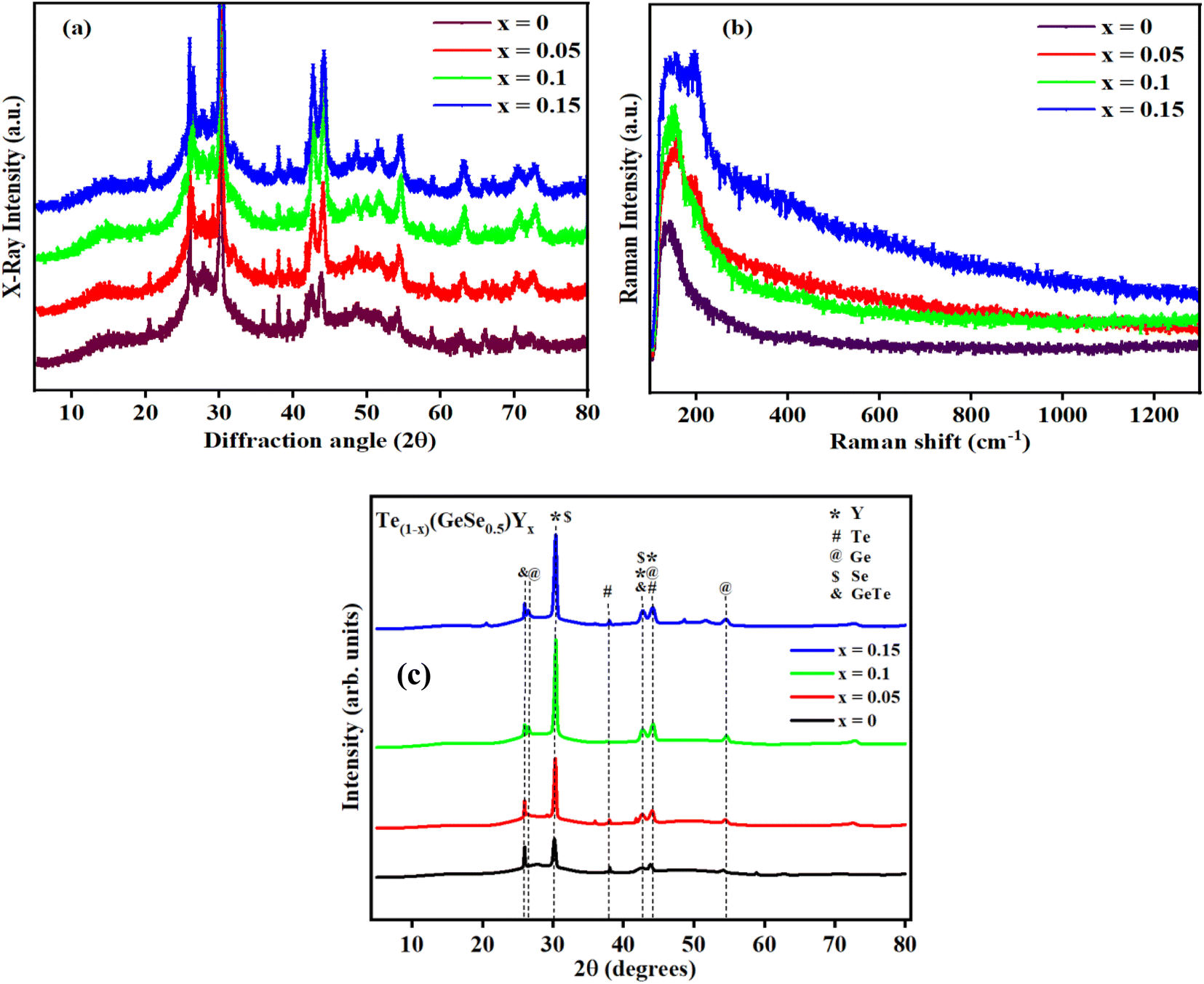 | ||
| Fig. 1 (a) X-ray diffractograms, (b) Raman spectra, (c) Rietveld refined XRD of Te(1−x)(GeSe0.5)Yx (x = 0, 0.05, 0.1, 0.15) thin-film samples. | ||
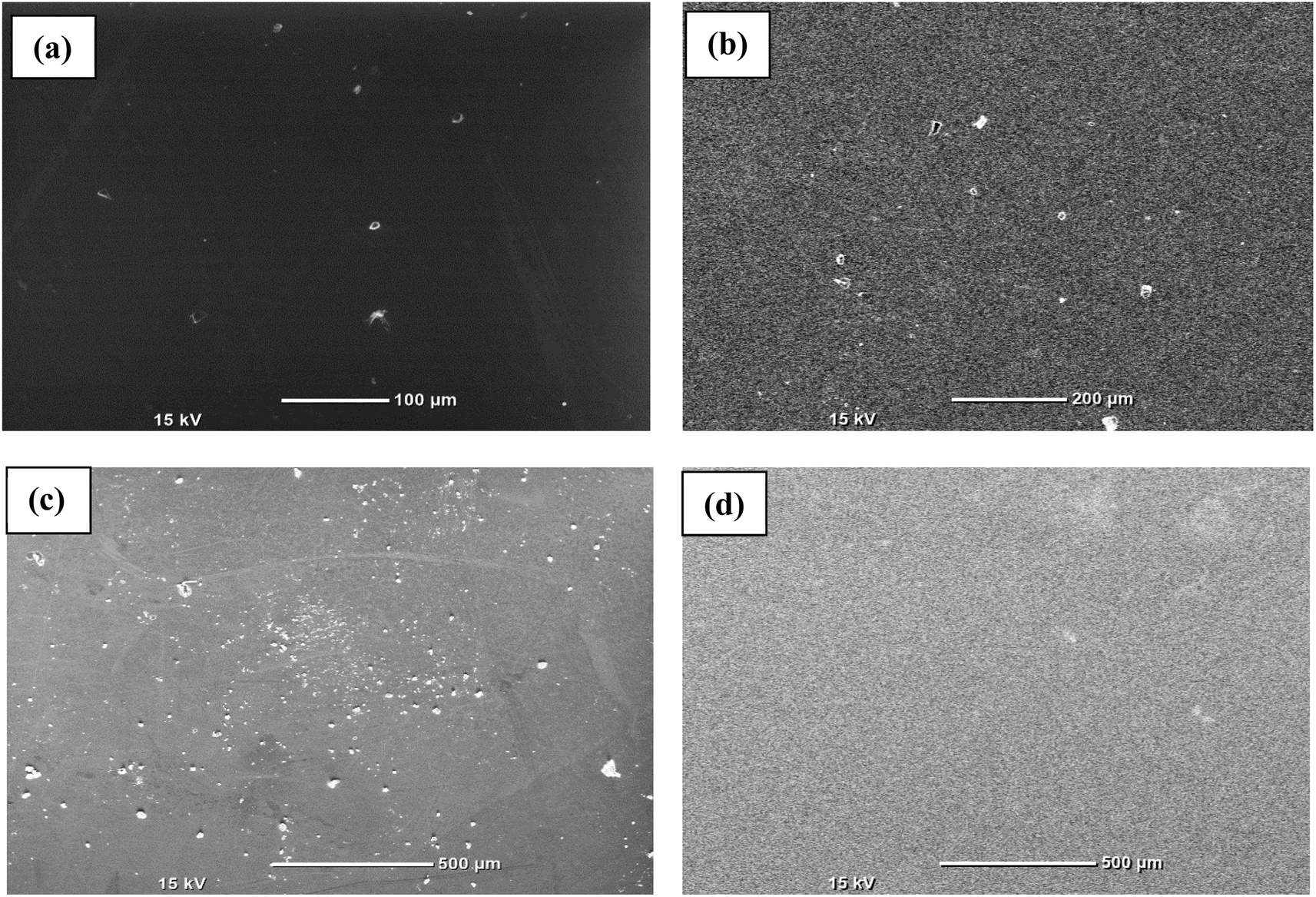 | ||
| Fig. 2 SEM images for surface morphological study of the Te(1−x)(GeSe0.5)Yx films. (a) x = 0, (b) x = 0.05, (c) x = 0.1, (d) x = 0.15. | ||
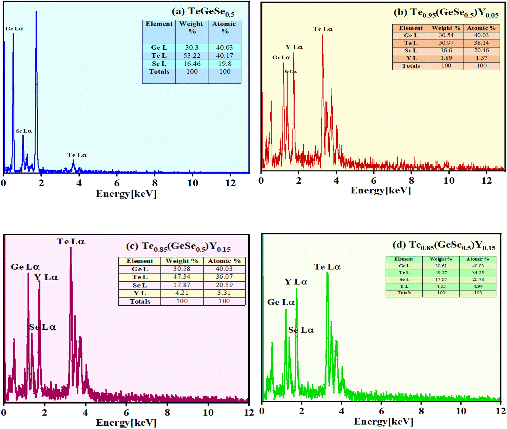 | ||
| Fig. 3 EDX spectra for the compositional study of the Te(1−x)(GeSe0.5)Yx thin films (a) x = 0, (b) x = 0.05, (c) x = 0.1, (d) x = 0.15. | ||
Raman spectroscopy, as depicted in Fig. 1(b), was employed to study the chemical formation, crystallinity, phase, and molecular interactions. Optical absorption spectra were recorded using a double-beam UV-visible spectrophotometer (Jasco V-770, FLH-741) within a 500–2500 nm wavelength range. In addition, IR transmission spectra were obtained utilizing an FTIR spectrophotometer (Shimadzu IRSpirit QATR-S FTIR spectrometer) in the range of 400 to 4000 per cm, with a resolution of 2 per cm. The linear and nonlinear optical characteristics were evaluated from the transmission spectra utilizing a variety of relationships.
3. Results and discussion
3.1. Structural analysis using XRD and Raman spectroscopy
Fig. 1(a) presents the XRD analysis for the Te(1−x)(GeSe0.5)Yx system with x values of 0, 0.05, 0.1, and 0.15. The diffraction angle 2θ was scanned from 10° to 80°. The XRD pattern of bulk Te(1−x)(GeSe0.5)Yx, as depicted in Fig. 1(c), illustrated the impact of Y substitution for Te. Initially, for GeTeSe0.5 (x = 0), the diffraction peaks precisely aligned with the standard pattern of ICSD23, indicative of a rhombohedral structure with minor traces of phase-segregated elemental Te. However, the effect of Y substitution became apparent through the broadening of the peak width and shift of the peak positions toward higher 2-theta values. The widening of the peaks indicated the increased Y content causing lattice distortion. The shift toward higher 2-theta values resulted from the compression of the lattice dimensions upon substituting the smaller Y atom for Te. This describes the analysis of the Se-substituted samples using Rietveld refinement with GeTeSe0.5 as a parent structure. The calculated and observed refinement patterns aligned well with the experimental measurements, indicating good agreement. The results, summarized in Table 1, reveal a systematic decrease in the lattice parameters, crystallite size, and volume for the Te(1−x)(GeSe0.5)Yx samples. The broadening of the peak full width at half maximum (FWHM) suggested a reduction in the coherent scattering domains, likely attributed to local distortion caused by Y's smaller atomic size within the GeTeSe0.5 structure.| Chemical formula | GeTeSe0.5 | x = 0.05 | x = 0.1 | x = 0.15 |
|---|---|---|---|---|
| Crystal system | Rhombohedral | Rhombohedral | Rhombohedral | Rhombohedral |
| Space group | R3m:H | R3m:H | R3m:H | R3m:H |
![[thin space (1/6-em)]](https://www.rsc.org/images/entities/char_2009.gif) |
||||
| Unit cell parameters Å | ||||
| a | 4.16872 | 4.14658 | 4.11887 | 4.07314 |
| b | 4.16872 | 4.14658 | 4.11887 | 4.07314 |
| c | 10.4781 | 10.3781 | 10.1973 | 10.2481 |
| c/a | 2.5135 | 2.5028 | 2.4757 | 2.5160 |
| Unit cell volume Å3 | 160.97420 | 158.72481 | 156.11487 | 155.37860 |
|
||||
| R values | ||||
| Rwp | 0.05674 | 0.06654 | 0.07167 | 0.03349 |
| RF2 | 0.06487 | 0.06741 | 0.08483 | 0.02471 |
| X2 | 1.997 | 1.8950 | 2.017 | 1.648 |
| Crystallite size (nm) | 32.7 | 30.9 | 28.6 | 27.9 |
Raman spectroscopy, as shown in Fig. 1(b), was conducted to investigate the chemical structure, phase, crystallinity, and molecular interactions of the samples. The vibrational mode observed at ∼160 cm−1 corresponded to the Ge–Te rhombohedral structure. It could be observed from all the spectra that there were negligible changes in the amorphous phase following Y doping.
3.2. Surface morphology study using SEM-EDX
Fig. 2 shows the SEM images of the thin films, showing the homogeneous deposition of the material on the substrate, indicating there was no cluster formation. Fig. 3 presents the EDX spectrum of the Te(1−x)(GeSe0.5)Yx system. The spectrum displayed maxima for the Ge, Te, Se, and Y elements, and their ratios were close to those of the nominal sample composition. Using k-factors for each element, it was estimated that the atomic percentage ratios in the analyzed alloy were approximately 40% Ge, 38% Te, 20% Se, and 2% Y. The error in estimating these elements did not exceed 2%.3.3. Study of the optical properties
Many optical features of semiconducting materials depend on understanding the optical absorption of the electromagnetic wave spectra, which is important fundamental knowledge. The extent of absorption of films may be impacted by numerous factors, including the composition of the film, doping components, doping ratios, and sample surface morphology. Thus, examination of the optical absorption and associated factors, for example, skin depth, optical density, extinction coefficient, and absorption coefficient, provides significant information. These parameters provide useful details regarding the characteristics and modifications of the electronics of the materials examined. For instance, it would be noteworthy to notice that the semiconductor material optical absorbance spectra show a sudden increase in specific photon energy. This increase might be related to electron changes that occur in the VB to CB.It should be mentioned that momentum and energy are conserved throughout the absorption process. At the semiconducting material's absorption edge, both direct and indirect transitions occur. The electrons in the VB undergo transit to the CB as a result of these transitions, which are caused by the interactions between electromagnetic waves and the electrons. In general, simultaneous interactions with the lattice vibrations are involved in the indirect transitions. As a result, in optical transitions, the electron wave vector may change.19,20 Therefore, in order to determine the transition type and the energy value of the optical bandgap of the current chalcogenide Te(1−x)(GeSe0.5)Yx (x = 0.05, 0.1, 0.15) thin-film samples, the research of optical absorption and absorption coefficient ‘α’ is given priority in the present investigation.
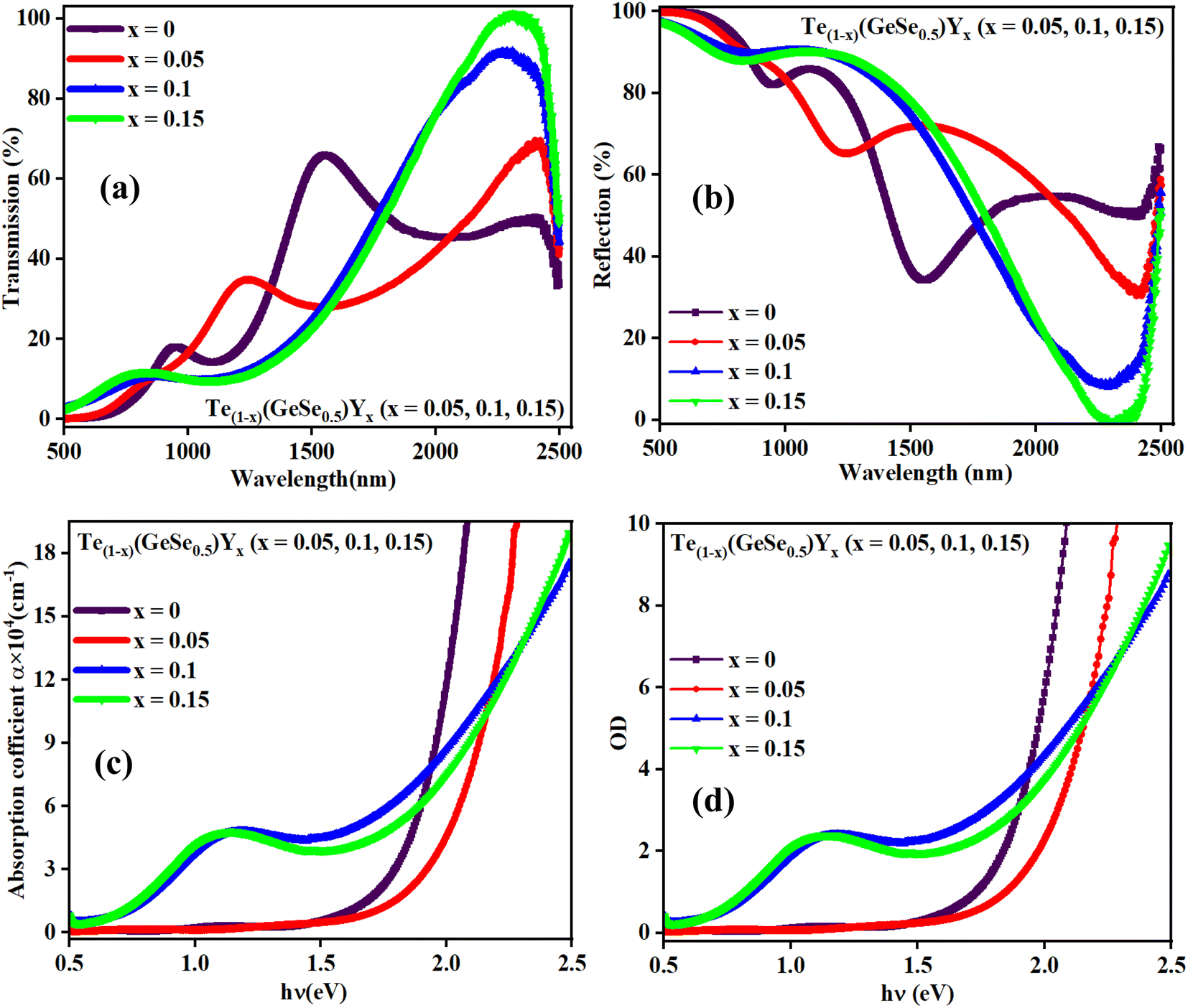 | ||
| Fig. 4 Variation in the (a) transmittance, (b) reflectance with wavelength, (c) absorption coefficient, and (d) optical density with the energy of the studied samples. | ||
Optical absorbance serves as a useful indicator offering insights into the bandgap and band structure of both amorphous and crystalline materials. The optical absorption edge arises from electronic transitions in the semiconductor. In this context, the region of the absorption edge fell within the scale of 500–1000 nm, and the absorption coefficient (α) was evaluated from the absorbance value utilizing the below equation:
 | (1) |
 | (2) |
The absorption capacity of the film is also indicated by another optical measure known as the optical density (OD). This indicates the extent to which a medium slows down transmitted light rays. The optical density is contingent upon the material concentration. It is associated with a subtle inclination of the atoms within the material to retain the absorbed energy from electromagnetic waves through vibrating electrons. This absorbed energy is subsequently re-emitted as a new disturbance for the propagating waves. Additionally, the dispersion of thin films, as indicated by their optical density, varies with thickness. Consequently, the velocity of electromagnetic waves is influenced by the optical density of the film material. As the optical density increases, the hindrance to the propagation of electromagnetic waves within the material intensifies. Fig. 4(d) illustrates the variation in OD (= α × t, where ‘t’ represents the film thickness and ‘α’ denotes the absorption coefficient), which increased with the Y incorporation. In thin films, the OD arises from the refraction and scattering of light, reflecting the speed of light within the material. The absorption is minimal (below 2%) at lower frequencies, leading to an improvement in electromagnetic wave transmission within a low-absorption range. This characteristic contributed to the high infrared (IR) transmission observed in Ge–Te–Se–Y chalcogenide thin films. Here, the optical density or the absorbance increased at higher energy values and it also increased with the Y content. For x = 0, the OD increased from 1.56 eV, to 1.63 for x = 0.05, 1.16 eV for x = 0.1, and 1.07 eV for x = 0.15. The optical density increased for x = 0.1 and 0.15 and it increased at lower values of energy compared to for x = 0, 0.05. The higher optical density was due to the bonding contribution of yttrium, where the bonding ratio Ge–Te/Ge–Y decreased with the Y content in the Ge–Te–Se–Y alloys. This behavior has been observed in other researchers' work also.22–24
In the spectral region with high absorbance, incident photon energy is absorbed by the semiconducting film. The penetration depth, also known as the skin depth (δ), is defined as the thickness of the film at which the optical density of the incident photon reaches 1/e of its value at the surface of the film. This depth of penetration is influenced by various parameters, including the film conductivity, material density of the film, and incident photon frequency, as well as the morphology of the film surface and its microstructure. The electrical and optical conductivities of semiconductors are contingent upon the optical bandgap energy and electronic transitions. Hence, there exists a correlation between the penetration depth (δ) of semiconductor films and their optical properties. The penetration depth or skin depth (δ) is related to the coefficient of absorption (α) through the equation:25,26 δ (cm) = 1/α. The relationship between the penetration depth (δ) and the photon energy incident on the Te(1−x)(GeSe0.5)Yx thin-film surface is depicted in Fig. 5(a).
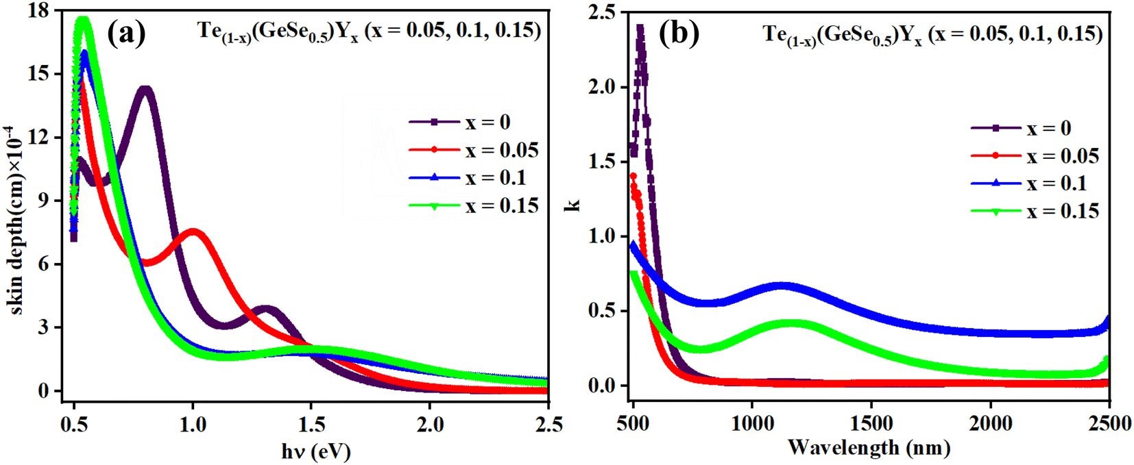 | ||
| Fig. 5 (a) Variation of skin depth ‘δ’ spectra with the photon energy, (b) dependence of the k-spectra with the wavelength for the Te(1−x)(GeSe0.5)Yx thin-film samples. | ||
It was observed that the penetration depth (δ) diminished with the incorporation of the Y content. This reduction in δ was correlated with an escalation in the absorbance of the film. Furthermore, during synthesizing, it was noted that the darkness of the films intensified with the increasing Y content. Additionally, the penetration depth decreased with the increase in the energy of the incident photons up to a certain value. The value of energy at which d becomes zero, observed across all the film samples, is termed the cut-off energy (Ecutoff), approximately amounting to 2 eV for the films under examination. The corresponding wavelength at this energy level is denoted as the cut-off wavelength (λcutoff), nearly equaling 623 nm for the current samples. Additionally, for photon energies exceeding the Ecutoff value (>2 eV), the penetration depth diminished (δ = 0), indicating the films' highest absorbance. Conversely, the propagated electromagnetic waves amplitude decreased at lower energies. Subsequently, the penetration depth (δ) demonstrated an increment toward the lower energy side, highlighting its strong dependence on the transmittance and reflectance values. This behavior aligns with previous findings reported in other work for similar semiconducting films.27,28
The rate at which electromagnetic waves travel through a material is dictated by the complex refractive index, typically represented as ñ = n − ik, where k stands for an optical parameter known as the coefficient of extinction, attenuation coefficient, or absorption index, while n indicates the refractive index. This optical constant, k, characterizes the reduction in the amplitude of incident electric-field oscillations. Consequently, the optical characteristics of the film material are influenced by the interaction between the electric-field component of the incident electromagnetic waves and the atoms of the material. Therefore, k plays a critical and foundational role in understanding the propagation of light waves through any material, as its value determines the extent of energy dissipation or loss due to absorption. The coefficient of extinction, k, can be expressed as k= (αλ/4π), where α represents the absorption coefficient and λ denotes the wavelength. Fig. 5(b) describes the spectral variation of this coefficient concerning the wavelength of incident photons. It displays there was a significant decrement in k values for the Te(1−x)(GeSe0.5)Yx films as the wavelength of the incident photons increased in the NIR region. The refractive index, extinction coefficient, and nonlinear parameters are all interconnected with the absorption coefficient. Its investigation holds significance primarily for estimating the propagation patterns of electromagnetic waves within the examined thin films with minimal damping or scattering. The k value explains the scattering, attenuation, or absorption of incident electromagnetic waves. Notably, the calculated lower k values and high transmission window render these materials highly suitable for near-infrared (NIR) and infrared (IR) optical applications. A similar behavior was observed by Mott and Davis29 in various other amorphous semiconductor materials. Additionally, the k value plays a vital role in dielectric studies.
| αhv = P(hv − Eg)m | (3) |
 | ||
| Fig. 6 (a) Evaluation of the indirect bandgaps of the studied films, (b) Eg and EU relationship. | ||
| Optical parameters | Te(1−x)(GeSe0.5)Yx | |||
|---|---|---|---|---|
| x = 0 | x = 0.05 | x = 0.1 | x = 0.15 | |
| Eg (eV) | 1.18 | 1.43 | 0.89 | 0.79 |
| P1/2 (cm−1/2 eV−1/2) | 165.87 | 158.61 | 151.37 | 144.28 |
| EU (eV) | 0.99 | 1.14 | 1.19 | 1.24 |
| σ × 10−2 (steepness parameter) | 18.45 | 17.02 | 16.39 | 15.14 |
| Se−p | 3.62 | 3.91 | 4.26 | 4.61 |
| Ed (eV) | 21.57 | 23.31 | 25.84 | 28.69 |
| Eo (eV) | 1.34 | 1.32 | 1.29 | 1.27 |
| f = Eo Ed | 28.90 | 30.76 | 33.33 | 36.43 |
| M−1 | 16.09 | 17.65 | 20.03 | 22.59 |
| M−3 | 8.96 | 10.12 | 12.03 | 14.01 |
| no | 3.89 | 3.91 | 3.95 | 3.98 |
| ε∞ | 23.23 | 26.65 | 28.03 | 30.59 |
| λo (nm) | 642.71 | 684.09 | 734.28 | 788.35 |
| so (nm2 × 10−8) | 10.25 | 11.47 | 13.89 | 15.34 |
| εL | 3.67 | 5.84 | 6.15 | 8.79 |
| N/m* (× 1056) (m−3 kg−1) | 0.1556 | 0.1570 | 0.1684 | 0.1725 |
| Plasma frequency ωP (× 1014) | 3.98 | 3.57 | 3.24 | 3.07 |
| ηopt | 1.60 | 1.66 | 1.73 | 1.81 |
| χ1 (esu) | 1.1297 | 1.1314 | 1.1357 | 1.1387 |
| χ3 × 10⁻¹¹ (esu) | 2.7376 | 2.7625 | 2.7934 | 2.8147 |
| nT2 × 10−9 | 2.6355 | 2.6547 | 2.7089 | 3.0145 |
| nF2 × 10−10 | 4.0345 | 4.1983 | 4.3781 | 4.7365 |
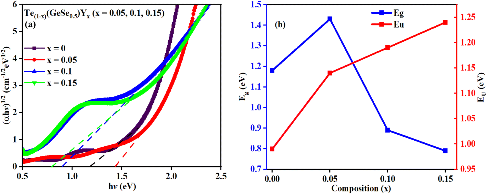
The value of Eg of the as-prepared film GeTeSe0.5 was 1.18 eV,17 which initially increased upon the doping of yttrium but then decreased as the Y doping increased. This can be explained by the Mott and Davis model.33 After doping, structural transformation takes place and the density of localized states increases in the gap, which decreases the bandgap.34,35 In another way, by the chemical bond approach, the formation of greater bond energy, such as for Y–Te (339 kcal mol−1) and Y–Se (435 kcal mol−1), was less than for Ge–Te (396.7 kcal mol−1) and Ge–Se (484.7 kcal mol−1). The temperature dependence of the bandgap in semiconductors is often associated with an increase in interatomic separation. This occurs because the magnitude of atomic vibration increases with a rise in thermal energy, leading to enhanced electron–lattice interactions. The P parameter indicates the degree of structural disorder for semiconducting materials. The P value was calculated from the slope of the graph shown in Fig. 6. The increasing value of P shows the reduction in the structural disorder.
Defects and impurities within a film can lead to a weak absorption region characterized by an exponential variation of ‘α’ with hv. This absorption edge signifies the presence of localized states within the gap. Band tailing arises from random variations in internal fields, leading to structural irregularities. The energy linked with this region is referred to as the Urbach energy (EU), which is calculated using Urbach's relation.
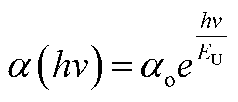 | (4) |
The broadening observed in the absorption edge is characterized by the steepness parameter (σ), attributed to excitation resulting from electron–phonon or excitation–phonon interactions. This parameter is determined by the relation σ = KT/EU, where T represents the temperature, EU denotes the Urbach energy, and K is the Boltzmann constant. The attained σ values are provided in Table 2, demonstrating the increase in σ with the increase in Y content. This observation confirmed the widening of the optical bandgap due to the broadening of the gap.
The strength of interaction between electrons and phonons is denoted by Se–p. Information regarding lattice expansion and the increment in lattice constants can be attained from Se–p. An increase in the Se–p value suggests an expansion in the lattice dimensions, and vice versa. Se–p is calculated using the formula Se–p = 2/3σ, as illustrated in Table 2. Considering that an increase in lattice dimensions leads to a decrement in the bandgap energy, there was a decrease in the Se–p value with the Y content. The decreased Se–p values correlate well with the higher Eg value due to their inverse relationship. Due to the unique optical characteristics of Ge–Te–Se–Y thin films, they are highly regarded for various optoelectronic applications and devices, including photonic circuits, photovoltaics, signal processing, solar cells, photolithography, optical fibers, and optical recorders.31
 | (5) |
Fig. 7(a) displays the refractive index variation with wavelength, displaying the normal dispersion nature of the film. The value of ‘n’ increased with the doping of Y, with a simultaneous increment in Eg. The value of ‘n’ was large at higher wavelength values, whereas it decreased at lower wavelengths. Absorption tends to be higher at higher frequencies, where the speed of light decreases, leading to an increase in the refractive index (n). This higher value of ‘n' facilitates greater optical field confinement, enabling switching in phase-change materials. Consequently, the optical intensities are enhanced, rendering the material more efficient and suitable for nonlinear interactions.21,38 The variation in refractive index is correlated with changes in the bandgap, as per Moss's rule, where Egn4 remains approximately constant.30,31
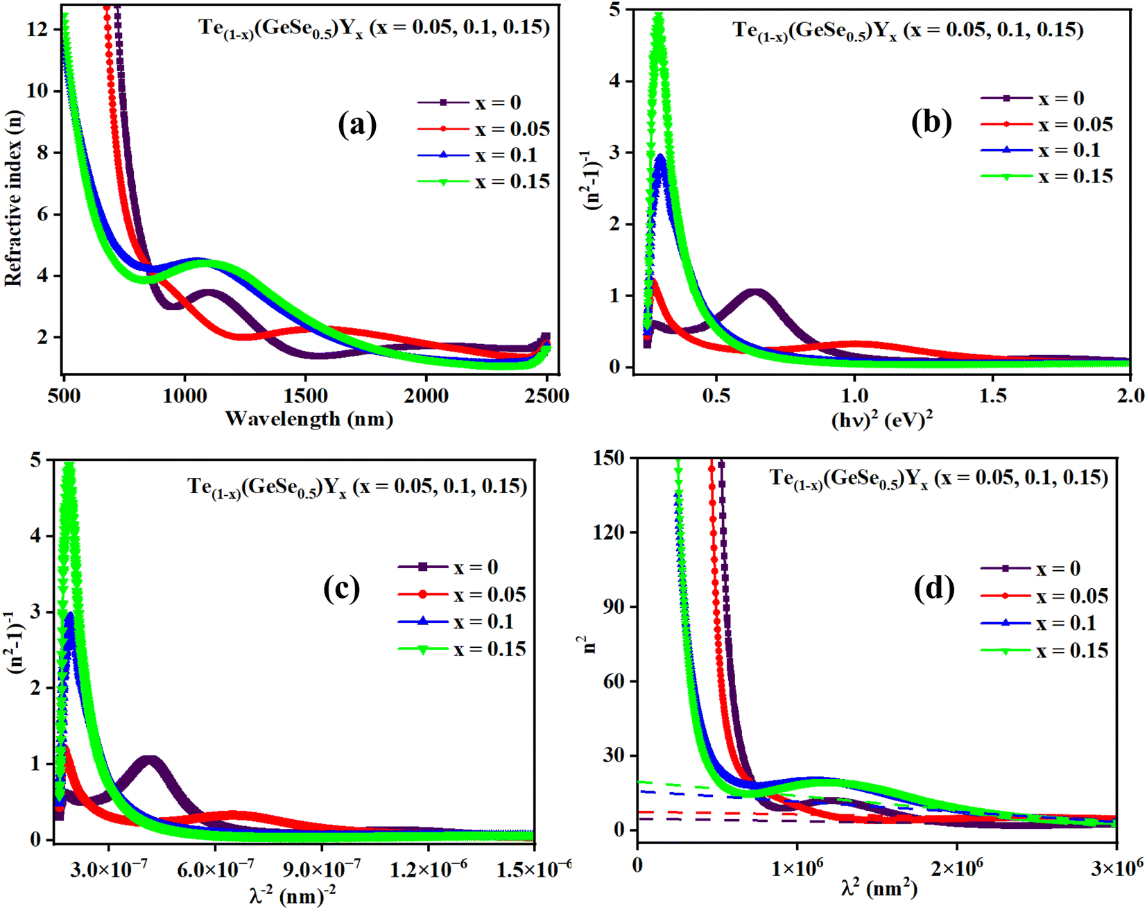 | ||
| Fig. 7 (a) Variation in ‘n’, (b) (n2 − 1)−1 versus (hv)2 plot, (c) (n2 − 1)−1 versus (λ)−2 plot, and (d) n2 versus (λ)2 plot for the Te(1−x)(GeSe0.5)Yx thin films. | ||
The dispersion parameters, particularly the single oscillator energy (Eo) and dispersion energy (Ed), are crucial for the design and functioning of spectral dispersion and optical communication devices. Two important parameters for optical devices are the single oscillator (Eo) and dispersion energy (Ed). Eo represents the single oscillator energy, which provides information about the band structure of a material, while Ed denotes the dispersion energy, which signifies the average interband optical transition strength. Ed is independent of Eo as it depends on the dielectric loss and on factors such as the structural parameters of a material. The Wemple–DiDomenico model relates Eo, Ed, and the energy of the incident photons (hv). Structural parameters that influence Ed include the coordination number (Nc), ionicity (β = 0.37 eV), effective number of valence electrons per anion (Ne), and anion valency (Za) of a material and these are related by Ed = βNcZaNe (eV). Ed is crucial for understanding the structural disorder and physical characteristics of a material. A decrease in Ed indicates a reduction in structural disorder, implying improved material properties.
The single effective oscillator model offers a comprehensive physical explanation of the measured parameters. This model is expressed by the following equation:30,31
 | (6) |
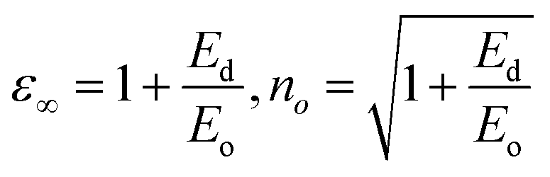 | (7) |
The quantity f = EoEd specifies the oscillator strength of a material, which was found to increase with the composition. ε∞ was noticed to decrease with the yttrium doping. The two factors of the spectra first-order (M−1) and third-order (M−3) were calculated by Eo and Ed by the below relations:30,31
| M−1 = Ed/Eo and M−3 = M−1/E2o | (8) |
The values of both M−1 and M−3 both decreased with the yttrium composition, as displayed in Table 1. In the lower frequency regime, the ‘n’ value follows the Sellmeier's dispersion model17,31 given below:
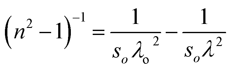 | (9) |
The value of so (strength of oscillator) and λo (wavelength of oscillator) can be determined by a straight-line fitting of the graph between (n2 − 1)−1 and (λ)−2 (shown in Fig. 7(c)). Here, the values of so and λo decreased with Y addition, as displayed in Table 2 λo is inversely related to Eo, and Eo is directly proportional to Eg, which results in λo ∝ 1/Eg.
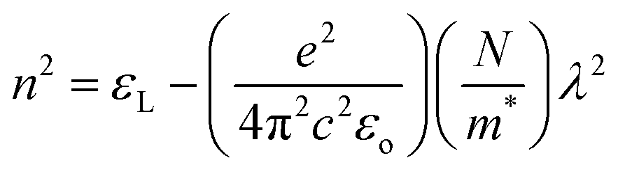 | (10) |
The plot depicted in Fig. 7(d), in correlation, facilitates the assessment of N/m* and εL, allowing deducing these values from the intercept and slope, respectively. The change in dipole orientation within the chalcogenide films resulted in variations in εL. Despite the close proximity of both the εL and ε∞ values, the decrease observed with the composition could be attributed to the increased polarization. The lower ε∞ value compared to εL was attributed to the contribution of free charge carriers to the polarization process, consistent with findings from previous studies.42,43
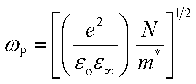
The plasma frequency (ωP) is calculated by using the Drude relation:17,44
 | (11) |
 | (12) |
The dielectric constant is an inherent property of a semiconductor that defines its behavior when subjected to an applied electric field. It comprises both real (εr) and imaginary (εi) parts, denoted as ε* (=εr + iεi). Furthermore, in terms of ‘n’ and ‘k’, it can be represented as ε* = (n + ik)2. The dielectric loss tangent (tanδ) is derived from εr and εi, where εr provides insights into the attenuation of incident energy during propagation within the films and is also related to the density of states (DOS) within the forbidden gap of a semiconductor material, while εi accounts for energy loss, referred to as the damping factor. This factor quantifies the energy dissipation within the material as light waves pass through it. The ratio of εi/εr assesses the loss factor, and these parameters are determined using the equation below :17,45
| εi = 2nk and εr = n2 − k2 | (13) |
Fig. 8(a) and (b) depicts the variation in εr and εi with wavelength, where it can be seen that both decreased with wavelength. The relatively higher value of εr compared to εi resulted from variations in ‘n’ and ‘k’. The dielectric loss factor quantifies the energy absorbed by the material as electromagnetic waves propagate through it. This parameter also illustrates the phase difference in energy loss at a fixed frequency (refer to Fig. 8(c)). Here, the value of ‘tanδ′ was higher at higher photon energy. The change in the nature of tan(δ) resembles that of the ‘k’ value, indicating the predominant influence of dielectric loss over optical absorption in this electromagnetic regime. The quality of oscillation, known as the quality factor (Q), is the reciprocal of tan(δ), i.e., Q = εr/εi. The Q factor was observed to decrease with the wavelength for the studied films, as depicted in Fig. 8(d).
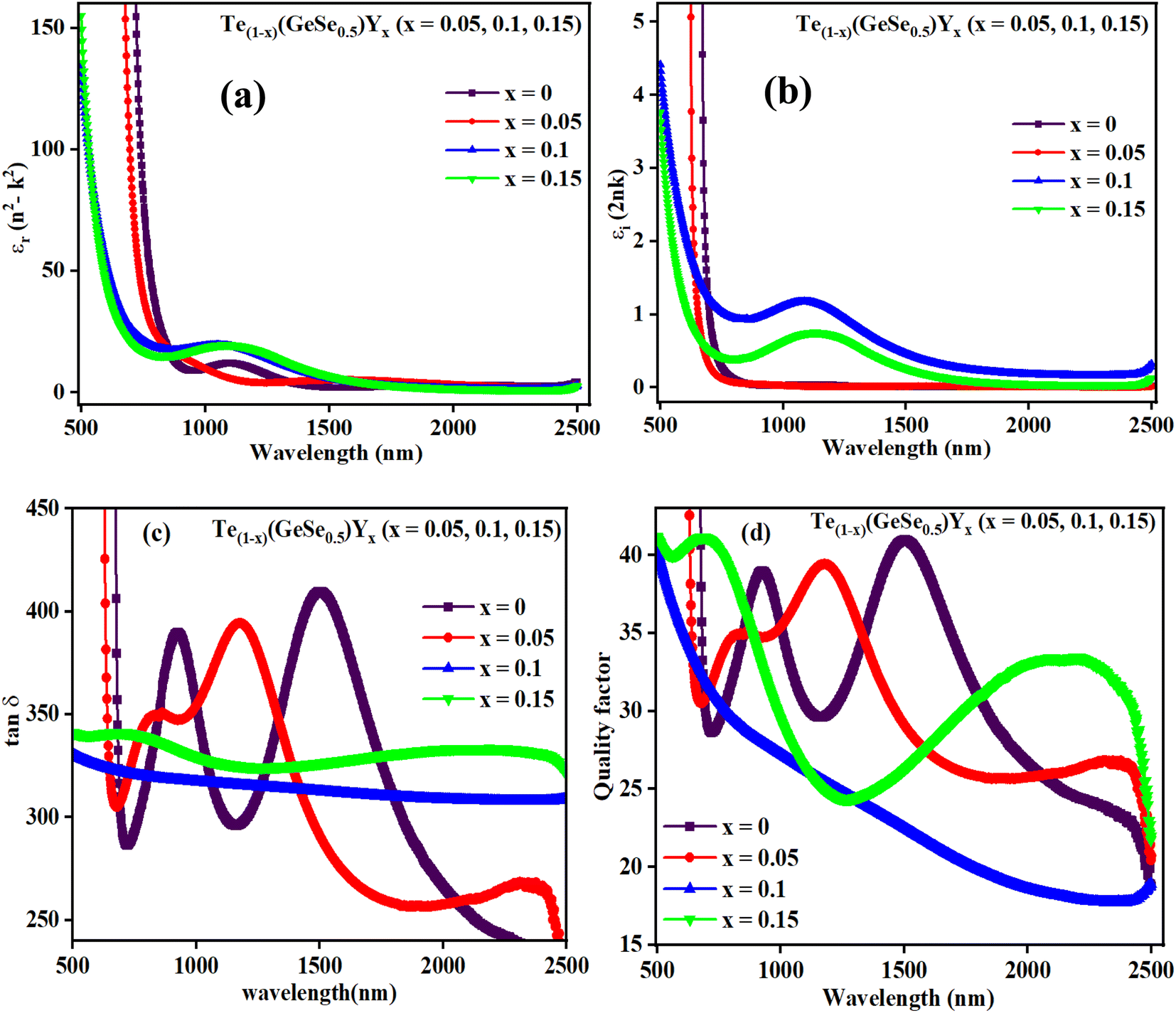 | ||
| Fig. 8 Plots of (a) εr, (b) εi, (c) tan(δ), (d) quality factor versus wavelength for the Te(1−x)(GeSe0.5)Yx thin films. | ||
When electrons move within a sample, they lose energy due to plasma oscillations induced in a sea of conduction band electrons. This energy loss is closely tied to the optical properties of the material. Energy loss parameters are crucial for understanding damping effects on the surface or within films. These functions help measure the average free path of inelastic electrons as they traverse through the sample. Therefore, it is vital to compute the volume energy losses (VELF) and surface energy loss functions (SELF). VELF and SELF are determined using εr and εi as follows:46
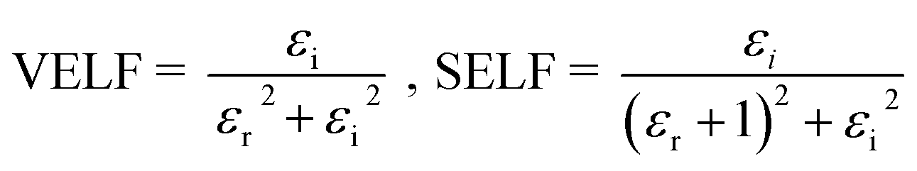 | (14) |
Both VELF and SELF characterize the absorption of energy in a material, indicating losses and are correlated with a single electron transition in a semiconductor. Fig. 9(a) and (b) display the variations in VELF and SELF with ‘hv’, illustrating that VELF and SELF decreased with hv.
 | ||
| Fig. 9 (a) Variation in VELF, (b) SELF, (c) σr, and (d) σi with hv for the studied films. | ||
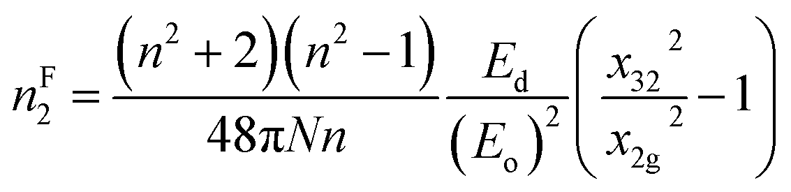
The electrical susceptibility (χc), i.e., the degree of polarization, is calculated by:
 | (15) |
The value of χc is displayed in Fig. 10(c), which displays an increasing trend with hv. The presence of lone pairs is associated with polarization by optical electronegativity (ηopt). The value of ηopt in terms of no is expressed as follows: ηopt = (C/no)1/4, where C = 25.54. The calculated ηopt values exhibited an increase with the composition for the studied films, as indicated in Table 2. Since ηopt is correlated with the refractive index, optical electronegativity also influences the nonlinear parameters.
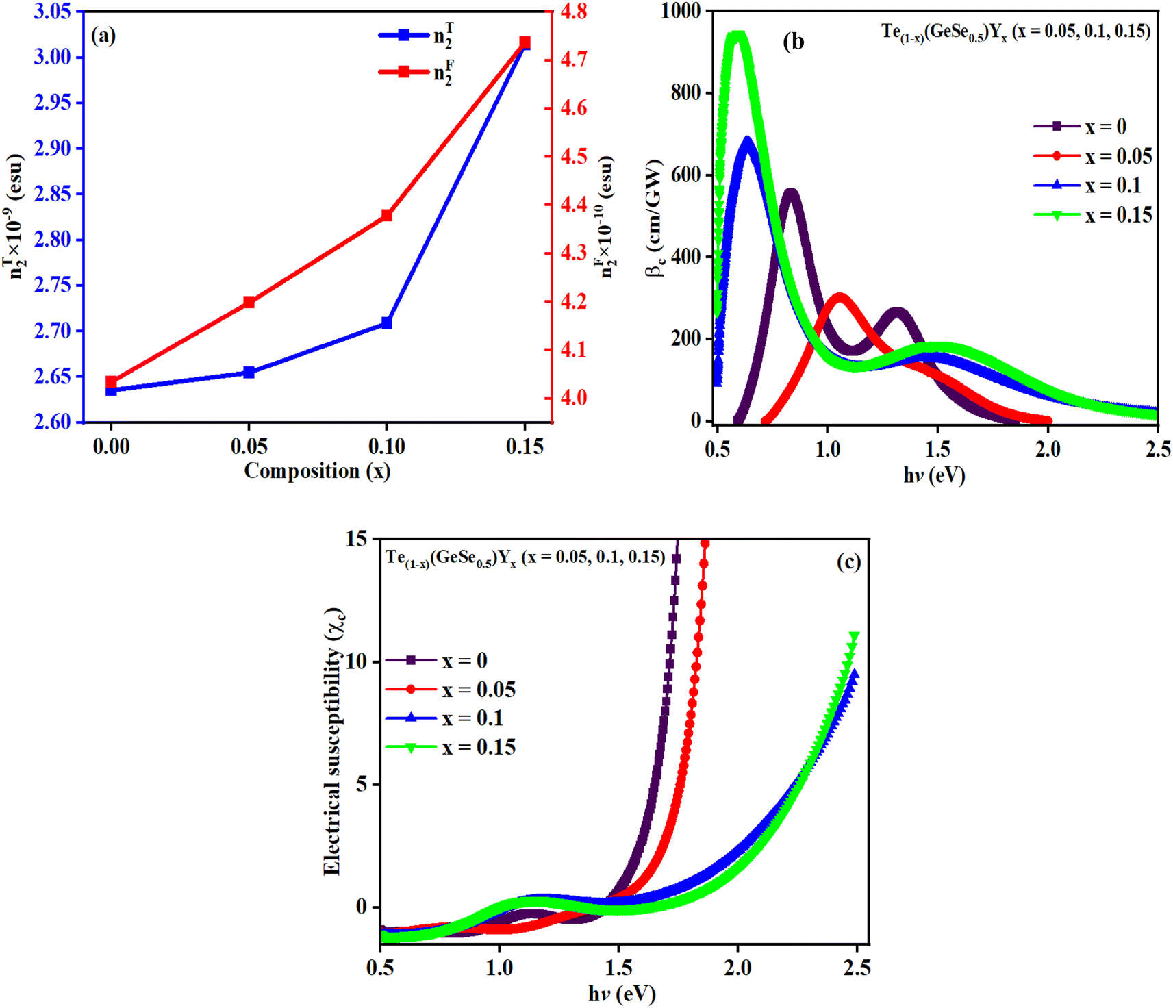 | ||
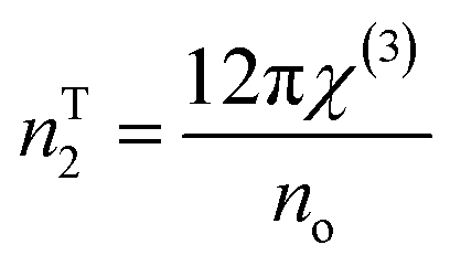
| Fig. 10 (a) nT2 and nF2 variation with the composition, (b) nonlinear absorption the coefficient βc, (c) electrical susceptibility (χc) variation with hv for the studied thin films. | ||
| P(t) = εo[χ1E(t) + χ2E(t)2 + χ3E(t)3 + …] | (16a) |
 | (16b) |
| χ3 = A(χ(1))4 | (16c) |
The nonlinear refractive index is determined from χ3 using the Tichy and Ticha formula:17,30,31
 | (16d) |
 | (16e) |
 | (16f) |
The estimated nF2 using the Fornier and Snitzer models is displayed in Table 2. Compared to nT2, nF2 exhibited a lower value. The comparative graph depicted in Fig. 10(a) illustrates that both nF2 and nT2 followed a similar trend to the linear refractive index, showing an overall decrease with the rise in wavelength. The number of homopolar bonds decreased with the increment in heteropolar ones, thereby reducing the defects in the band structure. Consequently, the reduction in defect density and variety accounted for the decrease in nonlinearity with the compositional variation. The decrease in χ3 and n2 by Y content is advantageous for solid-state lasers and UV nonlinear materials.30,31
Two-photon absorption (TPA) is a fundamental mechanism that elucidates the process of induced absorption within materials. This phenomenon occurs exclusively when the energy of incident light falls within the range of Eg/2 < hv < Eg. The TPA mechanism is characterized by the nonlinear absorption coefficient (βc), which can be determined using a straightforward empirical relation.17,31
 | (16g) |
4. Conclusion
The impact of Y concentration on various factors, including the structural and optical properties of Te(1−x)(GeSe0.5)Yx (x = 0, 0.05, 0.1, 0.15) chalcogenide thin films, was investigated. The energy bandgap (Eg) values were determined in the strong absorption region using the Tauc extrapolation method. The optical absorption outcomes of the selected system favor allowed indirect transitions. The evaluated optical bandgap was influenced by Y incorporation due to the higher binding energy of Te–Y compared to Te–Te binding energy. Additionally, the decreasing electronegativity contributed to the decrease in bandgap with Y concentration. The absorption coefficient followed the Urbach relation over a wide range of wavelengths, with calculated values of α indicating suitability for optical data-storage applications due to the high absorption coefficient. The decreasing k value with Y concentration indicated a reduced loss (εi = 2nk) due to increased energy absorption by the charge carriers. The nonlinear refractive index was evaluated using various methods, revealing the third-order nonlinear optical susceptibility χ(3) (∼10−10) and nonlinear refractive index n2 (∼10−9) increase with Y concentration. The results attained for Te(1−x)(GeSe0.5)Yx (x = 0, 0.05, 0.1, 0.15) thin films show they hold potential for various applications, including optical memory devices.Data availability
Data will be made available on request.Conflicts of interest
The authors declare no competing interests.Acknowledgements
Authors would like to acknowledge the contributions of numerous scientists and researchers whose work was extensively cited and whose insights greatly contributed to this paper.References
- C. Rios, M. Stegmaier, P. Hosseini, D. Wang, T. Scherer, C. D. Wright, H. Bhaskaran and W. H. P. Pernice, Nat. Photonics, 2015, 9, 725–732 CrossRef CAS.
- M. Mutailipu, K. R. Poeppelmeier and S. Pan, Chem. Rev., 2021, 121(3), 1130–1202 CrossRef CAS PubMed.
- M. Mutailipu, J. Han, Z. Li, F. Li, J. Li, F. Zhang, X. Long, Z. Yang and S. Pan, Nat. Photonics, 2023, 17, 694–701 CrossRef CAS.
- S. R. Ovshinsky, J. Non-Cryst. Solids, 1980, 42, 335–343 CrossRef CAS.
- S. R. Ovshinsky, Phys. Rev. Lett., 1968, 21, 1450–1453 CrossRef.
- N. Papandreou, A. Pantazi, A. Sebastian, M. Breitwisch, C. Lam, H. Pozidis and E. Eleftheriou, 2010 IEEE International Conference on Electronics, Circuits, and Systems, ICECS 2010 - Proceedings, 2010, pp. 1017–1020 Search PubMed.
- W. W. Koelmans, A. Sebastian, V. P. Jonnalagadda, D. Krebs, L. Dellmann and E. Eleftheriou, Nat. Commun., 2015, 6, 1–7 Search PubMed.
- R. E. Simpson, P. Fons, A. V. Kolobov, T. Fukaya, M. Krbal, T. Yagi and J. Tominaga, Nat. Nanotechnol., 2011, 6, 501–505 CrossRef CAS PubMed.
- S. Ghazi Sarwat, T. M. Philip, C. T. Chen, B. Kersting, R. L. Bruce, C. W. Cheng, N. Li, N. Saulnier, M. BrightSky and A. Sebastian, Adv. Funct. Mater., 2021, 31, 1–9 CrossRef.
- M. Nurmamat, K. Okamoto, S. Zhu, T. V. Menshchikova, I. P. Rusinov, V. O. Korostelev, K. Miyamoto, T. Okuda, T. Miyashita, X. Wang, Y. Ishida, K. Sumida, E. F. Schwier, M. Ye, Z. S. Aliev, M. B. Babanly, I. R. Amiraslanov, E. V. Chulkov, K. A. Kokh, O. E. Tereshchenko, K. Shimada, S. Shin and A. Kimura, ACS Nano, 2020, 14, 9059–9065 CrossRef CAS PubMed.
- S. Agarwal, P. Lohia and D. K. Dwivedi, J. Non-Cryst. Solids, 2022, 597, 121874 CrossRef CAS.
- S. Agarwal, P. Lohia and D. K. Dwivedi, J. Therm. Anal. Calorim., 2023, 10777–10793, DOI:10.1007/s10973-023-12440-6.
- S. Agarwal, P. Lohia and D. K. Dwivedi, Phys. B, 2022, 646, 414329 CrossRef CAS.
- M. Le Gallo and A. Sebastian, J. Phys. D Appl. Phys., 2020, 53, 213002 CrossRef CAS.
- A. V. Kolobov, P. Fons, A. I. Frenkel, A. L. Ankudinov, J. Tominaga and T. Uruga, Nat. Mater., 2004, 3, 703–708 CrossRef CAS PubMed.
- S. Agarwal, D. K. Dwivedi, P. Lohia and P. K. Singh, Ceram. Int., 2022, 50, 5483–5497 CrossRef.
- S. Agarwal, P. Lohia and D. K. Dwivedi, J. Non-Cryst. Solids, 2022, 606, 122199 CrossRef.
- S. Agarwal, P. Lohia and D. K. Dwivedi, New J. Chem., 2023, 47, 18957–18971 RSC.
- H. E. Atyia, S. S. Fouad, S. Kumar Pal, A. Srivastava and N. Mehta, Opt. Laser Technol., 2022, 150, 107985 CrossRef CAS.
- D. C. Sati, A. Dahshan, H. H. Hegazy, K. A. Aly and P. Sharma, Surface. Interfac., 2023, 39, 102995 CrossRef CAS.
- S. Agarwal, D. K. Dwivedi and P. Lohia, J. Alloys Compd., 2024, 983, 173773 CrossRef CAS.
- H. E. Atyia, S. S. Fouad, S. Kumar Pal, A. Srivastava and N. Mehta, Opt. Laser Technol., 2022, 150 DOI:10.1016/j.optlastec.2022.107985.
- H. P. Pathak, N. Shukla, V. Kumar and D. K. Dwivedi, Opt. Mater., 2016, 52, 69–74 CrossRef CAS.
- S. K. Pal, N. Mehta, H. E. Atyia and S. S. Fouad, J. Non-Cryst. Solids, 2021, 551, 120399 CrossRef CAS.
- S. K. Pal, N. Mehta, H. E. Atyia and S. S. Fouad, J. Non-Cryst. Solids, 2021, 551, 120399 CrossRef CAS.
- A. Zakery and S. R. Elliott, J. Non-Cryst. Solids, 2003, 330, 1–12 CrossRef CAS.
- A. Zakery and S. R. Elliott, J. Non-Cryst. Solids, 2003, 330, 1–12 CrossRef CAS.
- A. V. Kolobov, P. Fons, A. I. Frenkel, A. L. Ankudinov, J. Tominaga and T. Uruga, Nat. Mater., 2004, 3, 703–708 CrossRef CAS PubMed.
- E. A. Davis and N. F. Mott, Philos. Mag., 1970, 22, 903–922 CrossRef CAS.
- S. Das, D. Alagarasan, S. Varadharajaperumal, R. Ganesan and R. Naik, Adv. Mater., 2022, 3, 7640–7654 RSC.
- S. Giri, P. Priyadarshini, D. Alagarasan, R. Ganesan and R. Naik, RSC Adv., 2023, 13, 24955–24972 RSC.
- A. M. Abd-Elnaiem and G. Abbady, J. Alloys Compd., 2020, 818, 152880 CrossRef CAS.
- N. F. Mott, E. A. Davis and R. A. Street, Philos. Mag., 1975, 32, 961–996 CrossRef CAS.
- M. Mohamed, S. Moustafa, A. M. Abd-Elnaiem and M. A. Abdel-Rahim, J. Alloys Compd., 2015, 647, 771–777 CrossRef CAS.
- R. Chauhan, A. K. Srivastava, A. Tripathi and K. K. Srivastava, Prog. Nat. Sci.: Mater. Int., 2011, 21, 205–210 CrossRef.
- A. M. Abd-Elnaiem, S. Moustafa, A. M. Abdelraheem, M. A. Abdel-Rahim and A. Z. Mahmoud, J. Non-Cryst. Solids, 2020, 549, 120353 CrossRef CAS.
- A. M. Abd-Elnaiem, A. Z. Mahmoud and S. Moustafa, Opt. Mater., 2021, 111, 110607 CrossRef CAS.
- G. Abbady and A. M. Abd-Elnaiem, Phase Transitions, 2019, 92, 667–682 CrossRef CAS.
- M. Frumar, J. Jedelský, B. Frumarová, T. Wágner and M. Hrdlička, J. Non-Cryst. Solids, 2003, 326–327, 399–404 CrossRef.
- A. A. Abuelwafa, S. Elnobi, I. Yamada, N. Shibata and T. Soga, Opt. Mater., 2022, 123, 111850 CrossRef CAS.
- P. Sharma and S. C. Katyal, J. Appl. Phys., 2010, 107, 113527 CrossRef.
- A. A. Abuelwafa, M. S. A. El-sadek, S. Elnobi and T. Soga, Ceram. Int., 2021, 47, 13510–13518 CrossRef CAS.
- P. K. Singh and D. K. Dwivedi, Impact of Heat Treatment on the Structural and Optical Properties of Ge 4 Se 60 Te 30 in 6 Phase Change Thin Film, 2019, vol. 17 Search PubMed.
- S. K. Pal, N. Mehta, H. E. Atyia and S. S. Fouad, J. Non-Cryst. Solids, 2021, 551, 120399 CrossRef CAS.
- K. Yadav, R. Sangwan, Poonam, D. Mohan and S. Sanghi, J. Mater. Sci.: Mater. Electron., 2023, 34 DOI:10.1007/s10854-023-10559-8.
- W. Sun, Y. Lu, L. Miao and Y. Zhang, Photonics, 2022, 9, 132 CrossRef CAS.
| This journal is © The Royal Society of Chemistry 2024 |