DOI:
10.1039/D4RA05079G
(Paper)
RSC Adv., 2024,
14, 26437-26456
Numerical analysis and device modelling of a lead-free Sr3PI3/Sr3SbI3 double absorber solar cell for enhanced efficiency
Received
14th July 2024
, Accepted 16th August 2024
First published on 22nd August 2024
Abstract
Halide perovskites are the most promising options for extremely efficient solar absorbers in the field of photovoltaic (PV) technology because of their remarkable optical qualities, increased efficiency, lightweight design, and affordability. This work examines the analysis of a dual-absorber solar device that uses Sr3SbI3 as the bottom absorber layer and Sr3PI3 as the top absorber layer of an inorganic perovskite through the SCAPS-1D platform. The device architecture includes ZnSe as the electron transport layer (ETL), while the active layer consists of Sr3PI3 and Sr3SbI3 with precise bandgap values. The bandgap value of Sr3SbI3 is 1.307 eV and Sr3PI3 is 1.258 eV. By employing double-graded materials of Sr3PI3/Sr3SbI3, the study achieves an optimized efficiency of up to 34.13% with a VOC of 1.09 V, FF of 87.29%, and JSC of 35.61 mA cm−2. The simulation explores the influence of absorber layer thickness, doping level, and defect density on electrical properties like efficiency, short-circuit current, open-circuit voltage, and fill factor. It also examines variations in temperature and assesses series and shunt resistances in addition to electrical factors. The simulation's output offers valuable insights and suggestions for designing and developing double-absorber solar cells.
1. Introduction
The use of renewable energy sources, most notably solar power, is becoming more widely acknowledged as a viable way to meet the world's energy needs while also potentially reducing the adverse ecological consequences of conventional coal-based electricity industries. The imperative for high-performance, cost-effective solar panel technology has intensified in the context of addressing climate change driven by fossil fuel consumption.1 Recently, inorganic perovskites have also been studied since they could be very helpful as materials for solar cell absorbers.2–8 However, the inherent bandgap of absorber materials poses a limitation on light absorption, constraining single-junction solar cells from reaching their theoretical efficiency limit, known as the Shockley–Queasier limit. The decrease in performance of single-junction solar cells is primarily attributed to the lack of absorption of photons with energies beneath the bandgap. Additionally, the conversion of photon energy into carriers, rather than generating unfettered electron–hole duos, leads to heating defeats, further diminishing device productivity without enhancing results. To circumvent the Shockley–Queisser limit, researchers are concentrating on double-absorber solar panels, aiming to strengthen device efficiency. While one-layer perovskite solar cells may demonstrate higher effectiveness in certain scenarios, double-absorber configurations offer avenues for efficiency improvement. Typically, the integration of two absorber layers aims to broaden the absorbance range of perovskite solar cells (PSCs) to establish a hybridization.
During this context, Zhang et al. introduced a dual-absorber solar cell constructed on CsPbIxBr3−x/FAPbIyBr3−y, achieving a power conversion efficiency (PCE) of 17.48%.9 AlZoubi et al. conducted successful research on dual-absorber solar panels, achieving an increased 19.40% efficiency.10 Using CdTe/FeSi2, Rahman et al. created a numerical design for a double absorber solar cell that produced a noteworthy 27.35% power conversion efficiency.11 Abedini-Ahangarkola et al. utilized SCAPS-1D to investigate the superior effectiveness of perovskite/perovskite dual-absorbing solar cells, achieving a total effectiveness of 30.29%.12 Organometallic lead halide perovskite solar cells (PSCs) have garnered recent interest as a silicon-free solar power generating alternative to supplement conventional silicon photovoltaics.13,14 Lead-based perovskites are safer than other materials; however, there are stability issues with them. Still, a lead-free alternative for PSCs that shows promise is tin-halide perovskites.,15 offering potentially higher theoretical power conversion efficiency, enhanced carrier mobilities, and improved light absorption compared to their lead-based counterparts.16 Notably, perovskites based on NaZnBr3, such as NaZn0.7Cu0.3Br3, have been developed to address stability and efficiency issues.17 Sr3PI3 and Sr3SbI3 perovskites were deeply analyzed by the researchers in previous works and they showed that these materials will be very much effective for solar cell applications.18,19 Reza et al. introduced that above 28% PCE was achieved by using Sr3SbI3 perovskite as absorber in their work.20 Therefore, researchers have gotten above 27% PCE by using Sr3PI3 perovskite as absorber in their published work.21 Sr3PI3 and Sr3SbI3 have various benefits when used as absorbers in solar cells that are based on perovskites. To begin with, these materials have good visible-spectrum optical absorption, which is essential for effective solar energy harvesting. Additionally, because of their great chemical stability, the devices are less likely to break down over time and are more resilient. Sr3PI3 and Sr3SbI3 are non-toxic, addressing health and environmental issues, in contrast to lead-based perovskites. Their easy production and integration into current solar cell topologies are facilitated by their straightforward cubic crystal structures. These materials can also be optimized to maximize solar performance because of their tunable bandgaps. Last but not least, their energy and manufacturing costs are decreased by their compatibility with low-temperature processing methods. So, we have tried to expand the performance of Sr3PI3 and Sr3SbI3 perovskites based solar cells by arranging double absorber structure.
The ETL layer (n-type) is essential to the devices' JSC and VOC. The VOC is greatly impacted by the band orientation at the absorber/buffer interface. The conduction band offset (CBO) allows us to classify the sort of band orientation at the moment of interaction as either cliff, plane, or spike. Interface recombination is inhibited by an interface spike; however, interface recombination is increased and VOC levels are decreased by cliff-type band stretching.22 In order to prevent blocking the electrons' passage from the absorber layer into the ETL layer, which would reduce the fill factor and current density, the spike's amplitude must be sufficiently minimal.23 ZnSe (zinc selenide) is chosen as the charge carrier transport layer in this photovoltaic cell due to its favorable electronic properties, such as a suitable bandgap (∼2.7 eV), which allows it to act as an efficient ETL. ZnSe exhibits reduced absorption losses due to its strong electron mobility and good transparency in the visible range. Furthermore, efficient electron extraction is facilitated while back-transfer of holes is prevented due to its conduction band alignment with absorber materials such as Sr3SbI3. Additionally, ZnSe creates stable interfaces between the absorber layer and the FTO substrate, promoting strong adhesion and lowering interface recombination losses. Its appropriateness for these kinds of solar applications is further enhanced by its chemical stability and simplicity of manufacture. After depositing ZnSe using pulsed laser deposition (PLD) and analyzing the exceptionally preserved ZnSe layers optically and electrically, the bandgap, carrier concentration, and electron affinity in the ZnSe layers were determined.
Typically, the integration of two absorber layers aims to broaden the absorbance range of perovskite solar cells (PSCs) to establish hybridization. To our knowledge, the novel PSC prototype featuring the Sr3PI3/Sr3SbI3 heterojunction, which we intend to explore in this study, has not been previously investigated. Employing the SCAPS-1D software, we aim to model the behavior of this PSC setup with a heterojunction. Using the SCAPS-1D modelling instrument, a new dual-absorber solar cell was created and replicated, featuring a dual absorber layer composed of Sr3PI3 and Sr3SbI3 as the superior and inferior absorbers, respectively. Assumptions within SCAPS-1D include visually and electrically lossless tunnelling connections between the superior and inferior absorbers. The performance of this prototype during simulation is primarily influenced by the thicknesses of the absorber layers, doping concentrations, and defect densities. These variables are meticulously examined to assess their impacts on the electrical characteristics of the model. Additionally, we analyze the effects of temperature variations, shunt resistance, series resistance, and rear contact electrode on the electrical accomplishment of the novel PSC prototype based on Sr3PI3/Sr3SbI3. In the simulation, ZnSe is selected as the layer responsible for electron transport.
2. Device construction and simulation techniques
2.1 Structure of the device
FTO glass was used as the substrate for the hole transport layer (HTL)-free perovskite solar cells (PSCs), whereas ZnSe was used for the electron transport layer (ETL). and either Sr3PI3, Sr3SbI3, or a bilayer heterojunction of Sr3PI3/Sr3SbI3 as the light absorbance layer, with gold (Au) acting as the electrode. Fig. 1(a–c) illustrate the structures of these three types of PSCs. The layers of the suggested double absorber solar cell are as follows: Al/FTO/ZnSe/Sr3PI3/Sr3SbI3/Au, as depicted in Fig. 1(c). The proposed perovskites were named Device-I (Al/FTO/ZnSe/Sr3SbI3/Au), Device-II (Al/FTO/ZnSe/Sr3PI3/Au), and Device-III (Al/FTO/ZnSe/double absorber (Sr3PI3/Sr3SbI3)/Au). If we alternate the absorber positions (Al/FTO/ZnSe/double absorber (Sr3SbI3/Sr3PI3)/Au) in Device-III, the device performances are decreased (PCE = 31.98%, VOC = 1.04 V, FF = 85.55%, and JSC = 35.56 mA cm−2). All simulations were conducted under standard conditions: temperature of 300 K, frequency of 1.0 × 10⁶ Hz, and standard illumination of AM 1.5 G 1 sun. While data from literary sources was used to optimize other layer properties, simulation was used to determine the optimal thickness of the absorber layer. This arrangement creates a perfect tunnel with no optical loss or electrical resistance between the two absorbers. To mitigate shifting and protect the superior layers from solvent exposure and damage that sputters, dual-absorber solar cells include a conformal recombination layer amid absorber layers.
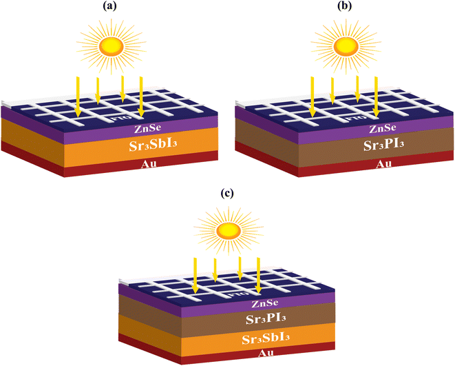 |
| | Fig. 1 Diagrammatic design configurations of (a) Device I, (b) Device II, and (c) Device III PV cells. | |
Table 1 lists the electrical parameters utilized in the simulations, with references to relevant computational and experimental studies found in the literature. Parameters such as layer thickness (t), relative dielectric constant (εr), electron affinity (χ), electron and hole mobility (μn & μp), bandgap (Eg), thermal velocity (vte, vtp), donor and acceptor densities (ND & NA), valence band and conduction band effective state densities (Nv & Nc), and total defect concentration (Nt) are included. Additionally, Table 2 presents the interface qualities of the ZnSe/Sr3SbI3, ZnSe/Sr3PI3, and Sr3PI3/Sr3SbI3 systems, allowing for the investigation of the impact of defect concentration while preserving a constant total defect density at the contact.
Table 1 SCAPS-1D simulation parameters for absorber, ETLs, and FTO
| Parameters |
Sr3SbI3 (ref. 20) |
Sr3PI3 (ref. 21) |
ZnSe24 |
FTO25 |
| Layer thickness, t (μm) |
0.5 |
0.5 |
0.05 |
0.05 |
| Band gap, Eg (eV) |
1.307 |
1.258 |
2.70 |
3.6 |
| Electron affinity, χ (eV) |
4.0 |
3.850 |
4.09 |
4.5 |
| Dielectric permittivity (relative), εr |
5.40 |
5.90 |
10.0 |
10 |
| Hole mobility, μh (cm2 (V−1 s−1)) |
50 |
25 |
20 |
20 |
| Electron mobility, μn (cm2 (V−1 s−1)) |
50 |
20 |
50 |
100 |
| VB effective density of states, NV (cm−3) |
2.4 × 10¹⁹ |
1.7 × 10¹⁹ |
1.5 × 10¹⁸ |
1.8 × 10¹⁹ |
| CB effective density of states, NC (cm−3) |
1.2 × 10¹⁹ |
1.03 × 10¹⁹ |
1.8 × 10¹⁹ |
2 × 10¹⁸ |
| Defect density, Nt (cm−3) |
1 × 10¹² |
1 × 10¹² |
1 × 10¹⁴ |
1 × 10¹⁴ |
| Shallow uniform acceptor density, NA (cm−3) |
1 × 10¹⁸ |
1 × 10¹⁸ |
0 |
0 |
| Shallow uniform donor density, ND (cm−3) |
0 |
0 |
1 × 10¹⁷ |
1 × 10¹⁸ |
Table 2 Characteristics of interface used in heterojunction solar cells comprising Al/FTO/ZnSe/absorber (Sr3PI3/Sr3SbI3)/Au structure
| Interface |
Defect type |
Capture cross section: electrons/holes (cm2) |
Defect position above the highest EV (eV) |
Reference for defect energy level |
Energetic distribution |
Total defect density (cm−2) |
| Sr3SbI3/ZnSe (Device-I) |
Neutral |
1 × 10⁻¹⁹ |
0.06 |
Above the highest Ev |
Single |
1.0 × 10¹⁰ |
| Sr3PI3/ZnSe (Device-II) |
Neutral |
1 × 10⁻¹⁹ |
0.06 |
Above the highest Ev |
Single |
1.0 × 10¹⁰ |
| Sr3SbI3/Sr3PI3 (Device-III) |
Neutral |
1 × 10⁻¹⁹ |
0.06 |
Above the highest Ev |
Single |
1.0 × 10¹⁰ |
| Sr3PI3/ZnSe (Device-III) |
Neutral |
1 × 10⁻¹⁹ |
0.06 |
Above the highest Ev |
Single |
1.0 × 10¹⁰ |
2.2 Simulation techniques
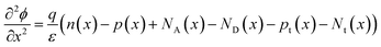
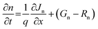
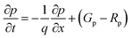
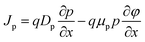
SCAPS-1D (version 3.3.0.7) is a sophisticated instrument for simulating solar cells, specifically crafted to examine the properties of individual layers in solar cells.26 Established by Mark Burgelman of the University of Gent, Belgium's Department of Electronics and Information Systems, this software is extensively utilized for analyzing different types of solar cells.27,28 It provides the PV community with detailed insights into parameters such as PCE, VOC, FF, and JSC (short-circuit current density) for each layer. Those functionalities are achieved through fixing three essential equations integrated into the SCAPS-1D software: the Poisson eqn (1), continuity eqn (2) and (3), and charge transport eqn (4) and (5), which govern the behavior of charge carriers. These equations are as follows:29,30| |
 | (1) |
In these equations, (q) represents the elementary charge, ε denotes the dielectric constant, (p) signifies the hole concentration, (n) represents the electron concentration, (ND) stands for the doping concentration of donor-type, and (NA) represents the doping concentration acceptor-type.
| |
 | (2) |
| |
 | (3) |
here, (
Gn) indicates the generation rate for electrons, (
Gp) denotes the generation rate for holes, (
Rn) represents the recombination rate for electrons, (
Rp) signifies the recombination rate for holes, (
Jp) represents the hole current density, and (
Jn) is the electron current density.
| |
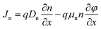 | (4) |
| |
 | (5) |
(
Dn) denotes the electron diffusion coefficient, (
Dp) signifies the hole diffusion coefficient, (
μn) represents the electron mobility, and (
μp) denotes the hole mobility.
Eqn (6) and
(7) illustrate the connection between important PV characteristics, as demonstrated below.
31| |
 | (6) |
| |
 | (7) |
In these equations, (Pin) represents the input solar energy, and (Pmax) denotes the maximum power output.
3. Result and discussion
3.1 Left contact work function's effect on solar cell performance
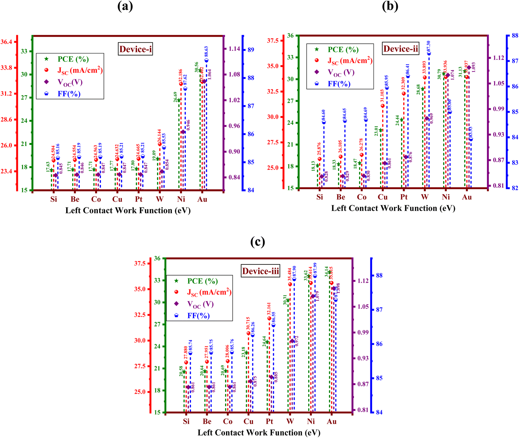
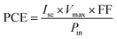
The productivity and general functioning of the solar panel are affected via the left contact, which has a substantial influence on the cellular performance.32 To maximize efficiency, the left contact, which is usually a component of the electrical contacts that extract current, needs to have low resistive losses. Inadequate contact may result in higher series resistance, which lowers power output and current flow. To preserve stability and endurance, it must also guarantee strong adhesion and little chemical contact with the semiconductor. Inadequately engineered connections may result in shading effects, obstructing light, and decreasing the active area. Improved charge carrier collection and reduced recombination losses are two benefits of optimal left contact design that directly impact the effectiveness and dependability of the solar panel. The best metal for the left contact is chosen by comparing its work function, which ranges from 4.85 eV to 5.47 eV. Fig. 2(a–c) display the PV parameters that were obtained for Devices I, II, and III with various left contacts. It has been observed that with gold (Au) as the left contact, we have gotten maximum performances from Devices I, II, and III. Once Au and Al were chosen as the left and right contacts, respectively, we observed maximum PCE values of 30.56, 31.13, and 34.14%, FF values of 88.63, 83.93, and 87.29%, JSC values of 32.402, 33.936, and 35.615 mA cm−2, and VOC values of 1.064, 1.074, and 1.098 V for Devices-I, II, and III. Table 3 shows the properties for front and back contacts.
 |
| | Fig. 2 Variation of left contact metal for (a) Device-I, (b) Device-II, and (c) Device-III. | |
Table 3 Back and front contact parameters used in simulation
| Parameters |
Left contact (back) |
Right contact (front) |
| Surface recombination velocity of electrons (cm s−1) |
1 × 10⁵ |
1 × 10⁷ |
| Surface recombination velocity of holes (cm s−1) |
1 × 10⁷ |
1 × 10⁵ |
| Majority carrier barrier height (eV) relative to EF |
−0.1630 |
−0.2400 |
| Majority carrier barrier height (eV) relative to EV |
−0.2453 |
−0.2580 |
| Work function (eV) |
Au (5.47) |
Al (4.26) |
| Temperature (K) |
275–475 |
3.2 Band diagram
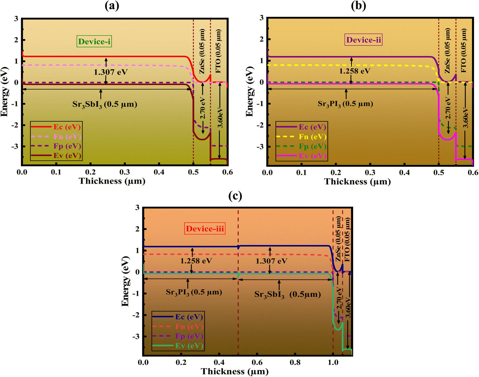
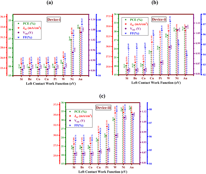
Fig. 3(a–c) depict three different kinds of HTL-free PSCs' band topologies, featuring different materials that absorb light (Sr3SbI3, Sr3PI3, Sr3PI3/Sr3SbI3) bilayer combination of the perovskite solar cells (PSCs), offering a comprehensive insight into their characteristics. Within this context, the symbols EC (eV), Fn (eV), EV (eV), and FP (eV) denote various energy levels within the band structure, namely denoting the valence band's maximum energy level, or the Fermi level for holes, the Fermi level for electrons, and the conduction band's minimum energy level, respectively. The discrepancy in energy levels between the lowest point of the conduction band (CB) electrons in the perovskite layer and the electron transport layer (ETL) is referred to as the conduction band offset (CBO), whereas the difference between the highest point of the valence band (VB) holes in the perovskite layer and the hole transport layer (HTL) is termed the valence band offset (VBO). In this study, the bandgaps of Sr3PI3 and Sr3SbI3 perovskite materials are determined to be 1.258 eV and 1.307 eV, correspondingly. The fluorine-doped tin oxide (FTO) window layer's energy gap is measured to be 3.6 eV, while the n-type zinc selenide (ZnSe) ETL layer exhibits energy gaps (Eg) of 2.70 eV.
 |
| | Fig. 3 Band arrangement of three types of HTL-free PSCs, featuring different light absorber materials: (a) Sr3SbI3, (b) Sr3PI3, (c) Sr3PI3/Sr3SbI3 bilayer combination. | |
3.3 Absorption coefficient of all layers
An essential indicator of a material's capacity to absorb light energy is its optical absorption coefficient, which has a significant impact on a solar panel's power conversion efficiency (PCE).33,34 The initial absorption peak is especially important for solar cells since it shows the exact light wavelengths that a material can absorb.35–37 Materials such as Sr3PI3, Sr3SbI3, ZnSe, and FTO are related to the FTO/ZnSe/absorber (Sr3SbI3/Sr3SbI3) SC structure. Fig. 4 displays the variations in the absorption coefficient at different wavelengths for the materials Sr3PI3, Sr3SbI3, ZnSe, and FTO. The absorption coefficient for Sr3PI3 and Sr3SbI3 materials surprisingly exhibits high peaks at 200 nm wavelength, but the FTO material exhibits a peak at 174 nm wavelength. On the other hand, the absorption coefficient for ZnSe material surprisingly exhibits high peaks at the 210 nm wavelength. Each substance's optical absorption spectrum displays the maximum absorption sites in the visible and ultraviolet light spectrums. According to Fig. 4(a–d), the absorption peaks for Sr3PI3, Sr3SbI3, ZnSe, and FTO materials are 198![[thin space (1/6-em)]](https://www.rsc.org/images/entities/char_2009.gif) 956.35 cm−1, 193593.72 cm−1, 113827.57 cm−1, and 100000 cm−1, respectively. The following tactics should be taken into consideration to make sure that target materials with bandgaps of 1.258 and 1.307 eV exhibit enough light absorption in the visible range for high-performance solar cells.
956.35 cm−1, 193593.72 cm−1, 113827.57 cm−1, and 100000 cm−1, respectively. The following tactics should be taken into consideration to make sure that target materials with bandgaps of 1.258 and 1.307 eV exhibit enough light absorption in the visible range for high-performance solar cells.
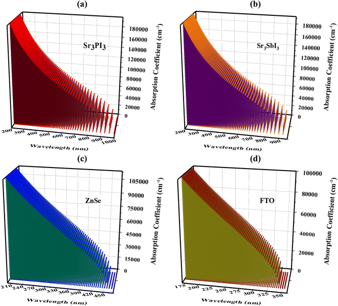 |
| | Fig. 4 Absorption coefficient of Al/FTO/ZnSe/absorber (Sr3SbI3/Sr3SbI3)/Au ideal solar cell construction for the following materials: (a) Sr3PI3, (b) Sr3SbI3, (c) ZnSe, and (d) FTO. | |
3.3.1 Doping and alloying. To move the absorption edge closer to the visible spectrum, modify the bandgap by doping or alloying with additional elements.
3.3.2 Layer thickness optimization. Optimize the thickness of the material layers to improve absorption of light while avoiding appreciable increases in recombination losses.
3.3.3 Antireflective coatings. To improve light absorption and decrease reflection losses, apply antireflective coatings to the surface of solar cells.
3.3.4 Light trapping structures. To improve absorption, include light-trapping structures in your material, such as photonic crystals or textured surfaces, which extend the light's travel length within it.In order to optimize the material's performance for solar cell applications, these techniques can aid in adjusting its optical characteristics.
3.4 Influence of the thickness, defect, and doping density of the single absorber layer
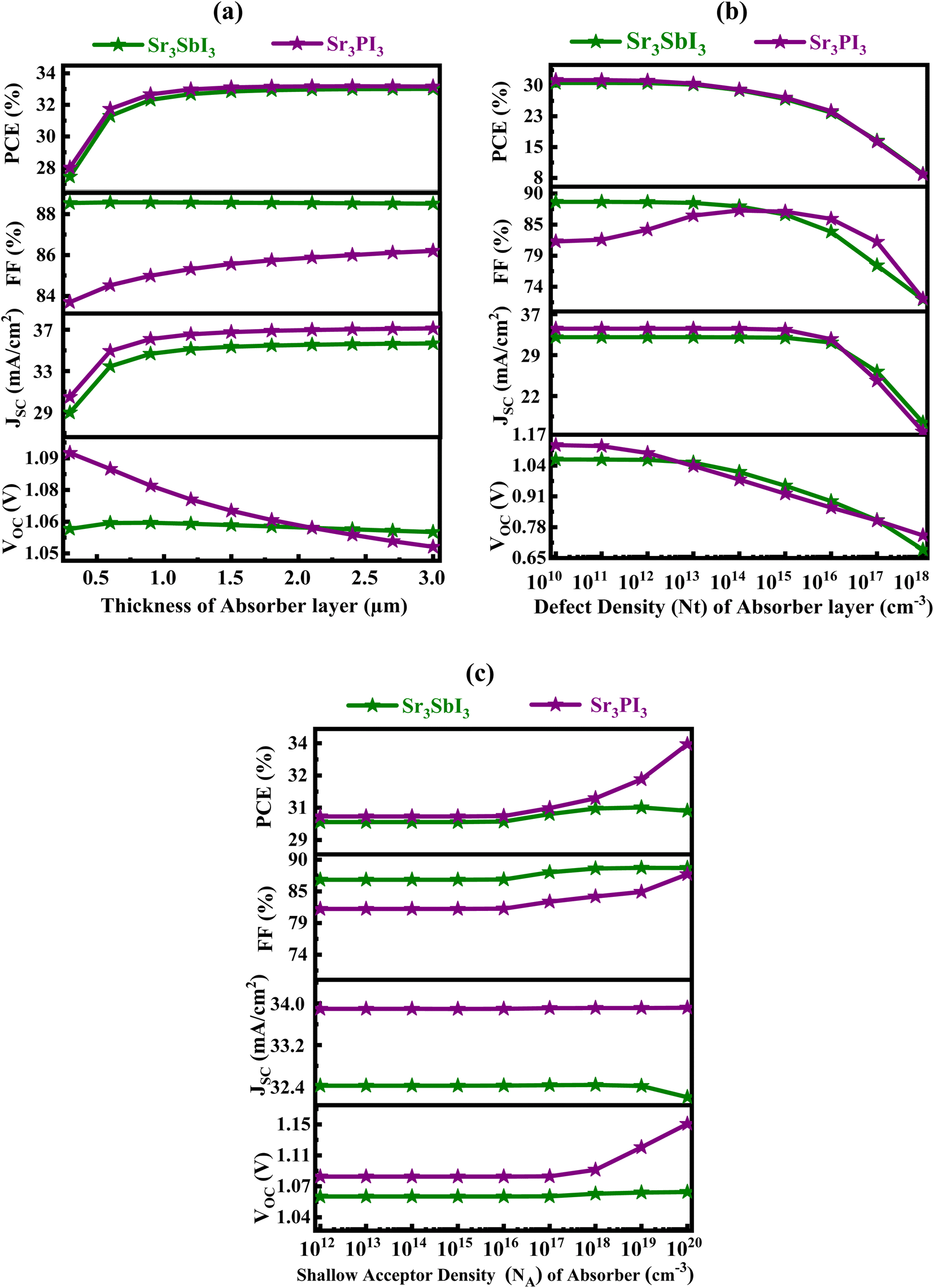
Fig. 5(a) illustrates the result of changing the absorber's thickness between three hundred and three thousand nanometers in order to figure out how to get the best results from our two simulated single absorber-based systems. An essential factor in increasing the efficiency of narrow-film photovoltaic cells is the thickness of the absorber layer.38 As soon as Device-II's absorber thickness increased during optimization, the reverse saturation current rose, but the VOC decreased even with a slight extension. However, with regard to device I, the variation in thickness barely affects the VOC. With thickness increasing, the spectral reaction grew at extended wavelengths, causing the JSC to rise and ultimately achieve an oversaturated value for all suggested gadgets. The thicker absorber in Device-II caused the structures to exhibit a noticeable FF rise, but in Device-I, it was constant. For devices I and II, efficiency was increased by using the proper thickness of absorber on both sides of 1000 nm. As the absorber layer thickens, more photons are absorbed, and the rate of recombination rises.21 Therefore, the optimal thickness for the absorber in the investigation was found to be 1000 nm in order to improve execution for Device-I and II incongruous structures. The optimal thickness values for Device-I were determined to be 30.5559% for PCE, 88.63% for FF, 32.40222 mA cm−2 for JSC, and 1.063996 V for VOC. PCE of 31.1272%, FF of 83.9314%, JSC of 33.93652 mA cm−2, and VOC of 1.092819 V were measured for device II.
 |
| | Fig. 5 Impact of (a) thickness, (b) defect density, and (c) doping concentration of absorber layer on the solar cell's performance for Devices I and II. | |
Recombination may be triggered by changes to the absorber layer's defect density (Nt) in photovoltaic systems, impede the charge carriers' progress, and compromise the durability of the device; inconsistent defect allocation all over the absorber layer can affect optical properties that affect photon absorption and can also result in spatial differences in device performance; the only ways to maximize PV efficiency and reliability are to minimize fault density and ensure homogeneity in the absorber layer. The impact of the absorber layer's Nt on the PV characteristics at a thickness of 1000 nm is illustrated in Fig. 5(b). The consequences of Nt between 1010 and 1018 cm−3 on Devices I and II were also examined. In Devices I and II, PCE, FF, JSC, and VOC significantly reduced from 30.60 to 8.46% and 31.31 to 8.36%, 88.66 to 72.04% and 87.18 to 72.16%, 32.402 to 17.151 mA cm−2 and 33.936 to 15.546 mA cm−2, 1.065 to 0.684 and 1.126 to 0.745 V, respectively, even though Nt increased from 1017 cm−3. For the purposes of additional computations, 1012 cm−3 is chosen as the ideal Nt worth for the absorbers.
The absorber layer's acceptor density (NA) was adjusted from 1012 to 1020 cm−3 to evaluate the effect of the absorber's NA on the PV characteristics. Fig. 5(c) shows how JSC, VOC, PCE, and FF fluctuate according to the choice of NA. The PSC's JSC stayed consistent at an approximately set amount as the NA was raised during optimization. The hole's Fermi energy level collapses as the absorber layer's NA grows, increasing the VOC in Device-II but remaining constant in Device-I. The built-in potential grows as the absorber layer's NA expands, and the boost in charge separation is an additional consideration contributing to the development of VOC. However, when the absorber layer's NA value surpassed 1016 cm−3, the PCE and FF rose. Regarding the variant of NA from 1012 to 1020 cm−3, the maximum ideals obtained for the VOC, JSC, FF, and PCE were 1.066 V, 32.402 mA cm−2, 88.73%, and 30.61% for Device-I, and 1.147 V, 33.941 mA cm−2, 87.65%, and 34.14% for Device-II. As mentioned in the paper, this could be the outcome of a higher number of defect states due to an increase in the NA of the absorber stratum.
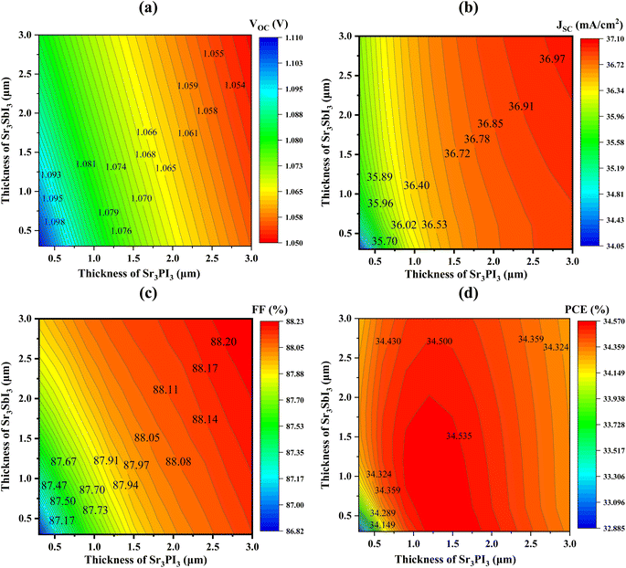
3.5 Impact of active layer thickness on the output parameters of double absorber device
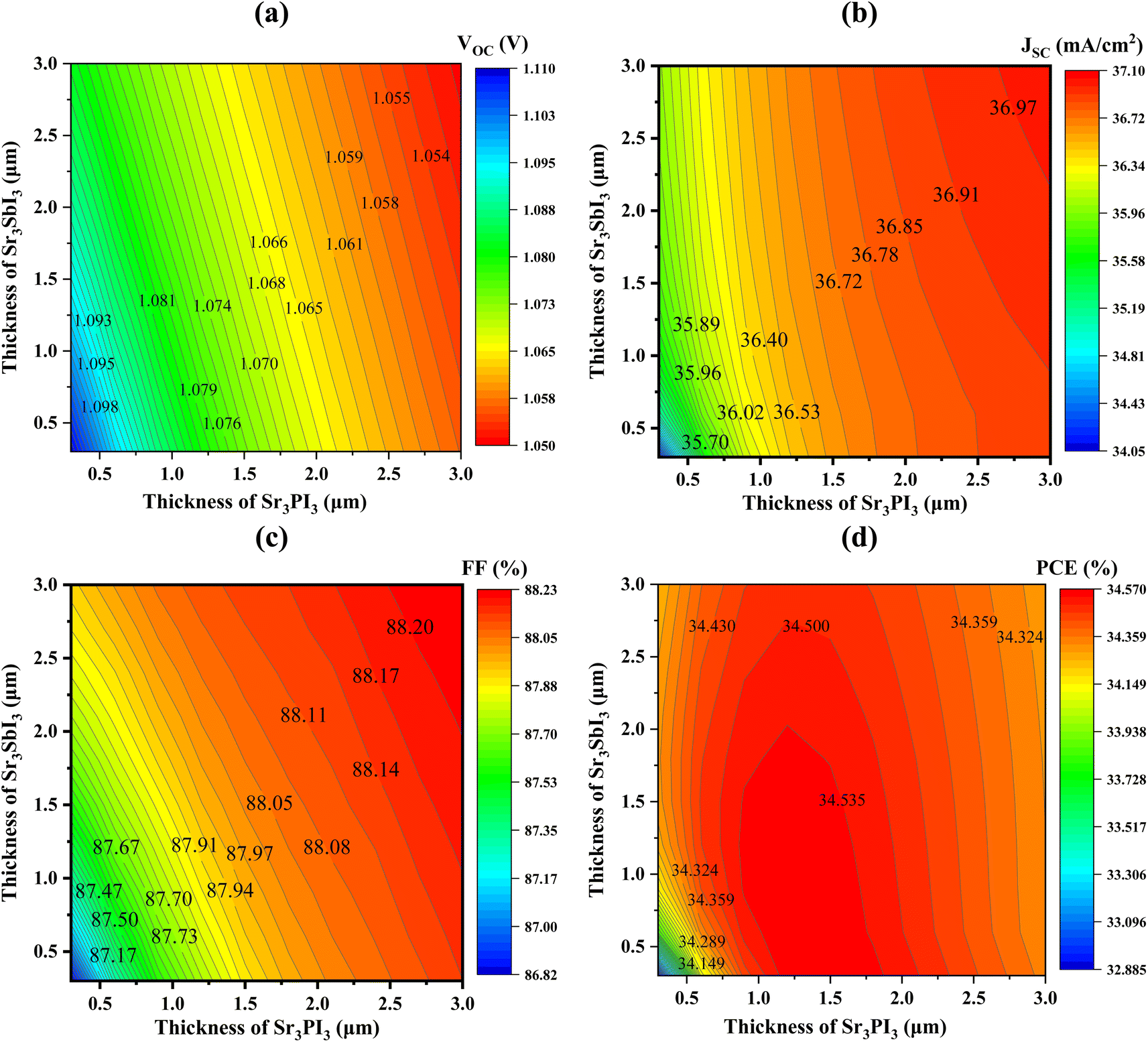
Fig. 6 illustrates the cumulative sway of the thicknesses of the double perovskite absorber layer (PAL). The x-axis represents the thickness of Sr3PI3, while Sr3SbI3 thickness is depicted on the y-axis. Through simulation models varying the PAL thicknesses from 300 nm to 3000 nm, the compatibility of different thickness combinations is evaluated, as depicted in Fig. 6(a–d). The photovoltaic (PV) outputs of the PSCs, or perovskite solar cells, are scrutinized to discern the optoelectrical qualities beneath AM 1.5G illumination. It is observed that the VOC peaks at smaller PAL thickness combinations, reaching up to 1.109 V, but declines with increasing PAL thickness due to heightened recombination rates. Concerning the short-circuit current density (JSC), a Sr3PI3 thickness of approximately 1 μm yields superior results, offering up to 36.97 mA cm−2. Conversely, lower thickness values of Sr3PI3 and Sr3SbI3 lead to reduced JSC due to inadequate photon absorption within the PALs, achieving around 34.12 mA cm−2, thereby adversely affecting efficiency. The contour plot in Fig. 6(c) demonstrates that a double PAL setup yields a maximum fill factor (FF) of 88.22% at variations in thickness values. Lastly, the collective impact of PAL thicknesses on power conversion efficiency (PCE) is depicted in Fig. 6(d), wherein an optimized value of 34.1395% is obtained using a combined thickness of 0.5 μm both for Sr3PI3 and Sr3SbI3. This aligns with the 35.61451 mA cm−2 JSC values under 0.5 μm and 0.5 μm absorber thickness, as PCE is directly proportional to JSC. The contour analysis furnishes valuable insights into PSC device investigations.
 |
| | Fig. 6 The electrical parameters, encompassing (a) VOC (b) JSC (c) FF and (d) PCE, as determined by altering the thickness of the both layers that are active. | |
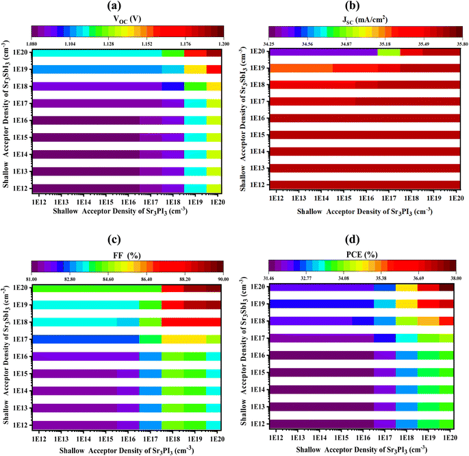
3.6 Effect of active layer doping concentration on the performance of double absorber device
The absorption layer within the perovskite material serves to capture photons released by light, thereby generating electron–hole pairs. Introducing doping to this layer has the potential to enhance carrier concentration, thereby aligning the energy bands of the hybridization with the electron transport layer and consequently enhancing solar cell performance. Our investigation delves into the impact of NA variation within the Sr3PI3 and Sr3SbI3 layers, spanning from 1 × 10¹² to 1 × 1020 cm−3. Fig. 7(a–d) elucidate the sway of NA on the electrical parameters of the two absorber layers. Notably, our findings indicate that the perovskite solar cell prototype exhibits superior performance when the NA level in the Sr3PI3 and Sr3SbI3 layers surpasses 1 × 1017 cm−3, as evidenced in Fig. 7(d).
 |
| | Fig. 7 Effect of active layer doping on electrical properties of PSCs: (a) VOC (b) JSC (c) FF and (d) PCE. | |
Indeed, when the NA in the Sr3PI3 layer exceeds that of the Sr3SbI3 layer, it facilitates enhanced mobility of holes and electrons within the absorber layer. The fill factor experiences significant influence from variations in NA, as depicted in Fig. 7(c). This variation in NA levels within the absorber layer instigates an internal electrical field, leading to substantial electron emission from the solar cell. Consequently, this phenomenon results in a reduction in voltage, as demonstrated in Fig. 7(a). Conversely, when the NA level in the Sr3SbI3 layer surpasses that of the Sr3PI3 layer, it impedes the flow of particles, causing the solar panel to function as an open circuit. Fig. 7(d) elucidates that the PCE of the PSC's highest points at a NA level of 1 × 1018 cm−3 for Sr3PI3 and 1 × 1018 cm−3 for Sr3SbI3 perovskite materials, achieving approximately 34.13% with a thickness of 500 nm and 500 nm for Sr3PI3 and Sr3SbI3, respectively. As NA increases, all electrical characteristics of the PSC improve except for the JSC. However, the VOC reaches 1.098137 V at the optimum NA of 1 × 1018 cm−3 for both Sr3PI3 and Sr3SbI3 perovskite materials (Fig. 7(a)). At the optimized NA for both PALs, the maximum JSC reaches 35.61451 mA cm−2 (Fig. 7(b)). Additionally, the FF reaches 87.2919% at this optimized NA (Fig. 7(c)).
3.7 Impact of active layer defect density on the performance of double absorber device
Fig. 8(a–d) depict the variance in defect density (Nt) within the perovskite absorber layer (PAL), spanning from 1 × 10¹⁰ to 1 × 1018 cm−3. Our findings reveal that Nt exerts a significant influence on the electrical parameters, as demonstrated in Fig. 8(a–d). The investigation focuses on both the Sr3PI3 and Sr3SbI3 absorber layers. Photovoltaic characteristics exhibit a decline with increasing Nt in the absorber layer, indicating a clear correlation between Nt and carrier trapping within the solar cell.39 Higher Nt accelerates carrier recombination by trapping carriers, resulting in energy loss as carriers collide within the crystal lattice, thereby facilitating recombination due to reduced carrier energy levels. The escalating recombination process with increasing trap density leads to a deterioration in PSC performance, potentially causing device overheating. Thus, maintaining Nt within acceptable limits, approximately 1012 cm−3, is crucial, based on acceptable current and voltage thresholds from both the Sr3SbI3 layer (1.307 eV) and the Sr3PI3 layer (1.258 eV).
 |
| | Fig. 8 Influence of active layer defect density on electrical properties of PSCs: (a) VOC (b) JSC (c) FF and (d) PCE. | |
Fig. 8(d) demonstrates that the PCE peaks at a Nt of 1 × 1012 cm−3 for both perovskite materials, reaching nearly 34.13% for a thickness of 500 nm for Sr3PI3 and 500 nm for Sr3SbI3 PALs. As Nt increases, all electrical characteristics of the PSC decrease. However, the VOC extends its peak value of 1.098137 V at a Nt of 1 × 1012 cm−3 for both perovskite materials (Fig. 8(a)). The JSC exhibits a continuous decrease with increasing Nt, sharply declining at elevated levels. At an optimized Nt of 1 × 1012 cm−3 for both PALs, the maximal JSC reaches 35.61451 mA cm−2 (Fig. 8(b)). Additionally, FF reaches 87.2919% at this optimized Nt (Fig. 8(c)).
3.8 Effects of the ETL's thickness and doping density
The thickness of the ETL layer significantly affects the power output of solar energy systems,40 as Fig. 9(a) illustrates. By allowing charged particles to travel more readily from the absorber layer towards the electrode, buffer layers improve the durability and effectiveness of these kinds of devices. The thickness of the ETL layer impacts a number of PV device qualities, comprising energy carrier recombination, light absorption, and resistance to layer-to-layer contact. More expansive band gaps and narrower ETL layers successfully transport virtually all incoming photons to the Sr3PI3/Sr3SbI3 absorber layers, increasing the absorption of light in the cells. The VOC and JSC for Devices I, II, and III stayed nearly constant at 1.063, 1.092, 1.098 V, and 32.397, 33.931, 35.601 mA cm−2, respectively, in spite of the rise in the thickness of the ETL stratum. For Device II, the FF and PCE values varied from 86.71% to 83.93% and 32.24 to 31.10%, but for Devices I and III, they were constant at 88.63%, 87.29%, and 30.54%, 34.12%, respectively.
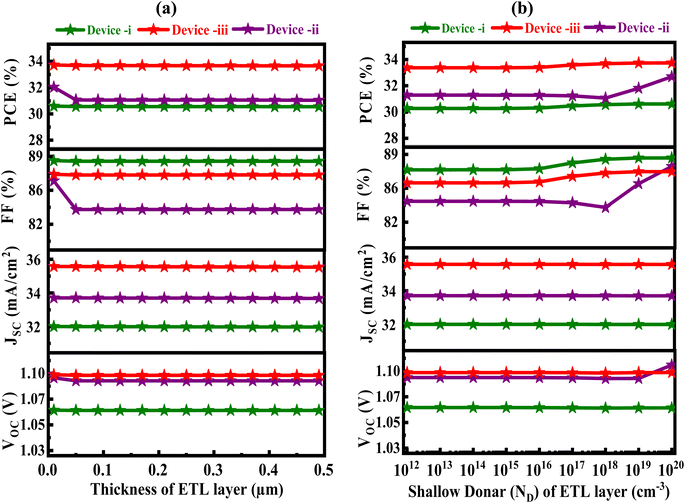 |
| | Fig. 9 Effects on the solar cell's performance caused by the (a) thickness and (b) doping level of the (ZnSe) electron transport layer, respectively. | |
Fig. 9(b) displays the PV qualities of Devices I, II, and III in relation to the donar concentration (ND) of ETL. As ND increased from 1012 to 1020 cm−3, FF and PCE for Devices I, II, and III stayed constant at 87.60, 84.53, 86.33%, and 30.22, 31.37, 33.78%. After that, there was a discernible rise in PCE and FF, from 30.22 to 30.60%, 31.37 to 32.99%, 33.78 to 34.20%, and 87.60 to 88.75%, 84.53 to 87.93%, 86.33 to 87.41%, respectively, for Devices I, II, and III. However, despite the rise in the ND of the ETL layer, the VOC and JSC for Devices I, II, and III remained almost unchanged at 1.064, 1.093, 1.098 V and 32.403, 33.938, and 35.615 mA cm−2, respectively. The ideal configuration was determined to be Devices I, II, and III with an ND of 1017 cm−3. This improvement in FF might possibly be attributed to the significant decrease in series resistance (Rs) and the increase in the internal electric field. The outcomes of this investigation are in line with earlier findings.41,42
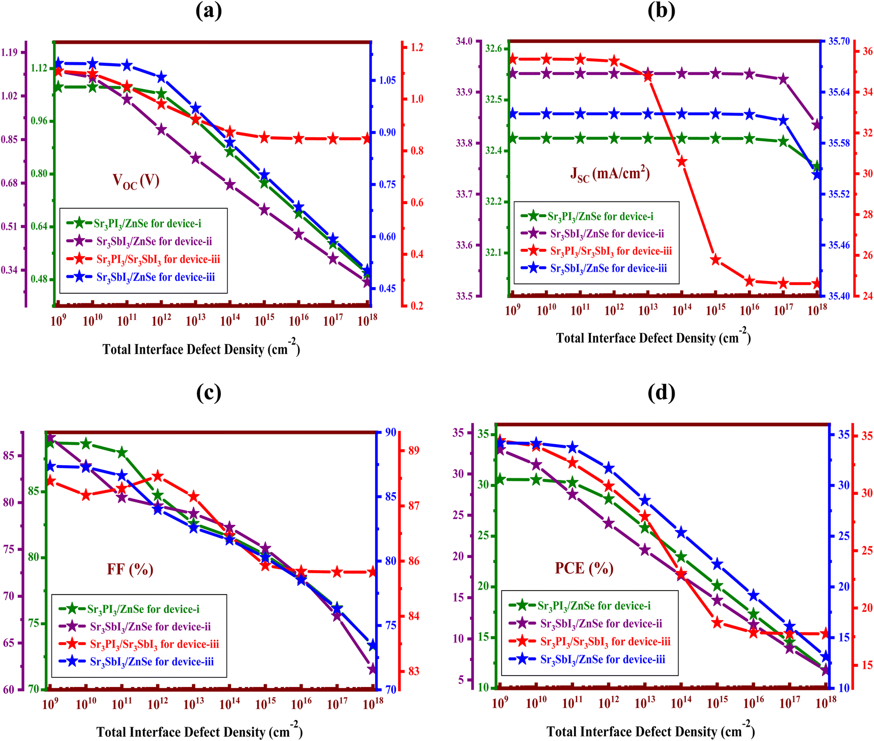
3.9 Impact of the interface defect density
Interface defects (Ntf) develop from structural flaws throughout the solar cell manufacturing process. These flaws worsen the effectiveness of the solar panel by promoting charge carrier recombination at the interface.43 For this reason, it is essential to evaluate their effects and choose the ideal parameters for realistic manufacturing. All simulations in this study used a neutral Ntf of 1010 cm−2 at the Sr3PI3/ZnSe (Device I), Sr3SbI3/ZnSe (Device II), Sr3PI3/Sr3SbI3 (Device III), and Sr3SbI3/ZnSe (Device III) interfaces, and all PV cells' defect levels were kept at 0.6 eV, as illustrated in Fig. 10. By changing the Ntf from 109 to 1018 cm−2, we may assess its impact on the PV parameters in this instance. PCE, FF, and VOC were significantly reduced with increasing Ntf from 30.58 to 11.82%, 88.70 to 73.33%, and 1.064 to 0.498 V for Sr3PI3/ZnSe (Device I), 32.94 to 6.17%, 86.94 to 62.20%, and 1.116 to 0.293 V for Sr3SbI3/ZnSe (Device II), 34.59 to 17.75%, 87.67 to 85.20%, and 1.107 to 0.846 V for Sr3PI3/Sr3SbI3 (Device III), 34.18 to 13.12%, 87.36 to 73.46%, and 1.098 to 0.502 V for Sr3SbI3/ZnSe (Device III). Recombination centers that are produced by Ntf can reduce the device's carrier transport efficiency, which lowers FF and VOC. But with increasing Ntf, JSC remained almost stable for all interfaces except the Sr3PI3/Sr3SbI3 (Device III) interface, where it reduced from 35.615 to 24.606 mA cm−2. Series resistance may rise substantially in the presence of interface difficulties.44 When Ntf increases, there is an increased rate of interface carrier recombination, which results in a decrease in performance.45,46 Consequently, it is suggested that a significant element affecting the performance attributes of PV devices is Ntf at the Sr3PI3/ZnSe (Device I), Sr3SbI3/ZnSe (Device II), Sr3PI3/Sr3SbI3 (Device III), and Sr3SbI3/ZnSe (Device III) interfaces.47,48
 |
| | Fig. 10 The impact of interface defect densities on the outputs of the PSC: (a) VOC (b) JSC (c) FF and (d) PCE. | |
3.10 Impact of the absorber layer's thickness on the G-R profile
Fig. 11(a) and (b) exhibit the carrier production and recombination rates for the Device I, II, and III structures over a wide range of locations. An electron forms duo of electrons and holes during carrier formation when it migrates from the valence band (VB) to the conduction band (CB), with the hole remaining in the VB.49 Sr3PI3 and Sr3SbI3 undergo this transition, releasing electrons and holes and producing additional carriers.50,51 Notably, the generation rate is lowest at around 1 μm and maximum at about 0.5 μm for Device I and II structured PSCs, but lowest at 1.04 μm and highest at roughly 1 μm for Device III. This mismatch results from different photon absorption rates at different places. Eqn (8) makes it easier to find G(x), and the SCAPS-1D model's Nphot (λ, x) evaluates the output of electron and hole duos based on the arriving photon flux.35| | |
G(λ, x) = α(λ, x)Nphot(λ, x)
| (8) |
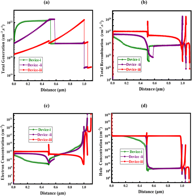 |
| | Fig. 11 Impact of (a) concentration of electron, (b) concentration of hole, (c) generation, and (d) recombination regarding the thickness of absorber layer. | |
In the conduction band of solar systems, electrons and holes recombine. In tastefully constructed and optimized PSCs, the density and durability of these charge carriers greatly influence the recombination rates. Each layer's defect states have a major impact on PSC recombination as well. When electrons cross the energy barrier, there are more of them that pair with holes in the valence band of the conduction band. Moreover, the energy levels associated with this transition affect the electron–hole recombination rates. Fig. 11(c) and (d) show the variations in absorber layer thickness, ETL, and their effects on electron and hole carrier concentrations. These differences in absorber thickness have an effect on the hole concentration in the absorber because they produce distinct densities of states (DOS) within the valence bands. Larger carrier concentrations are more significant, especially when comparing electron and hole densities dslb. This study indicates that the efficiency of the absorber material can be increased by utilizing ZnSe as the ETL in combination with the (Sr3PI3/Sr3SbI3) absorber, as this reduces electron–hole recombination and boosts carrier generation. These developments could pave the way for the development of PSCs that are incredibly successful.
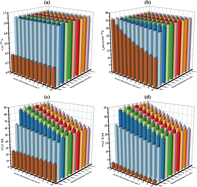
3.11 Influence of shunt and series resistances
Fig. 12 illustrates how the performance of solar panel parameters is impacted by both series (Rs) and shunt resistance (Rsh). Series resistance reflects the electrical hindrance caused by the connection of the device to external loads through its front and back contacts, while Rsh represents the leakage current occurring at the solar panel's edges. The Rs of a solar cell are determined by the circuit's overall impact of bulk resistance, both front and back metal contact resistance, and final resistance.52 In the study, Rs and Rsh were adjusted within the ranges of 0–10 Ω cm2 and 10–1010 Ω cm2, respectively. The analysis demonstrates that both series and shunt resistance play significant roles in determining the PCE, as depicted in Fig. 12(d). For the PSC to operate more efficiently, lower Rs and greater Rsh are necessary.53 Specifically, the VOC, illustrated in Fig. 12(a), exhibits a stronger correlation with lower values of shunt resistance rather than series resistance. Conversely, the JSC is more affected by higher values of series resistance compared to shunt resistance, as depicted in Fig. 12(b). Moreover, the FF demonstrates a notable dependency on changes in series resistance, as seen in Fig. 12(c). The data presented in Fig. 12 suggests that when the Rs and Rsh vary from 0 to 10 Ω cm2 and 10 to 1010 Ω cm2, correspondingly, the PCE, FF, JSC, and VOC change from 34.13% to 1.58%, 87.29 to 24.93%, 35.61 to 17.80 mA cm−2, and 1.098 to 0.356 V. These findings indicate that optimal PCE is achieved when the leakage current is minimized (elevated shunt resistance) and series resistance is minimized to facilitate effective carrier collection by the metal electrode.
 |
| | Fig. 12 Impact of shunt and series resistance on electrical properties of PSCs: (a) VOC (b) JSC (c) FF and (d) PCE for the optimum Al/FTO/ZnSe/double absorber (Sr3PI3/Sr3SbI3)/Au structure. | |
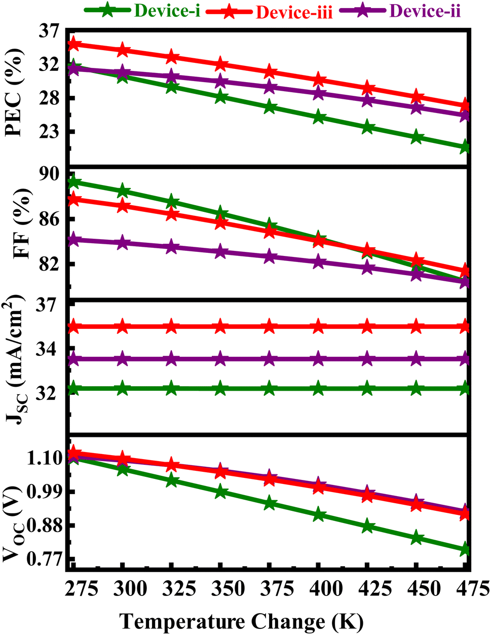
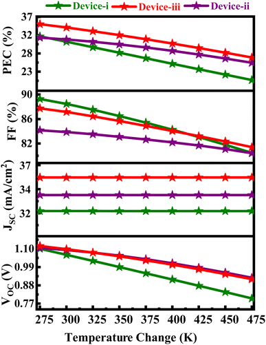
3.12 The impact of operating temperature on the performance of a solar cell
Fig. 13 illustrates how temperature affects Device I, II, and III's performance over a 275–475 K temperature range. The results reveal that as temperature increases, there's a tendency for JSC to stay stable while FF, VOC, and PCE decrease. This observation suggests that elevated temperatures enhance the thermal mobility of carriers within the solar panel, potentially leading to a higher JSC. However, increased temperatures may also cause the absorber layer to behave as an ohmic conductor, impeding carrier flow and resulting in the conversion of electrical energy into heat, thereby reducing FF, VOC, and PCE.54,55 The limited thermal dissipation within different components of the PSC can exacerbate temperature rise, posing a risk of device damage. Therefore, it is crucial to carefully consider the operational limits of each absorber layer during the creation of such interconnection solar cells. The temperature dependence is evident in the constant JSC values of 32.40, 33.93, and 35.61 mA cm−2, accompanied by a reduction in VOC from 1.100 to 0.801 V, 1.105 to 0.925 V, and 1.117 to 0.916 V for Devices I, II, and III. Conversely, FF decreases from 89.45 to 80.44%, 84.21 to 80.38%, and 87.88 to 81.39% for Devices I, II, and III, with increasing temperature. The efficiency reaches its highest value of 31.89, 31.58, and 34.97% at lower temperatures, declining to 20.88, 25.24, and 26.58% for Device I, II, and III as temperatures rise (see Fig. 13).
 |
| | Fig. 13 The effect of temperature changes on solar cells. | |
3.13 J–V and Q–E characteristics
A class of photovoltaic devices known for their cheap manufacturing costs and excellent efficiency is perovskite solar cells, which have drawn a lot of interest. The J–V (current density–voltage) and Q–E (quantum efficiency) qualities are two important aspects of these cells' operation to comprehend.18,19 The greatest current the cell can generate in an illuminated environment is shown by the current density at zero voltage. The voltage at which there is no current—the highest voltage that the cell is capable of producing. The ratio of charge carriers the cell accumulates to photons impinging on the cell is known as Q–E.56,57 It gauges the cell's capacity to transform incident photons into electrical current that can be used. The cell's efficiency is demonstrated throughout the solar spectrum by Q–E, which changes with the wavelength of incident light. This aids in the comprehension of the spectrum regions that the cell uses most efficiently. Q–E analysis can help guide advances in cell design by identifying losses resulting from non-radiative recombination, reflection, and transmission.
The J–V and Q–E qualities for Device-I, II, and III constructions are displayed in Fig. 14(a and b). With FF values of 88.63, 83.93, and 87.291%, JSC values of 32.40, 33.93, and 35.61 mA cm−2, and VOC values of 1.0639, 1.0928, and 1.0981 V, the optimized setup's PCE for Devices I, II, and III reached a maximum of 30.55, 31.12, and 34.13%. It is noteworthy that with regard to Devices I, II, and III, the current density of the optimized structure zeroes out at 1.08, 1.098, and 1.1 V. Remember that prior research has repeatedly demonstrated that current density declines with growing voltage,58,59 as Fig. 14(a) demonstrates. As seen in Fig. 14(b), the Q–E profiles cover a wavelength range of 300–1100 nm. For Device I, II, and III structures, the Q-E begins at around 100% and progressively drops to 0% as the wavelength gets closer to 950, 990, and 990 nm. This drop in Q–E correlates with the J–V profile conclusions. Table 4 summarizes the optimized simulated outputs for the final solar cells so that they can be further compared with earlier works.
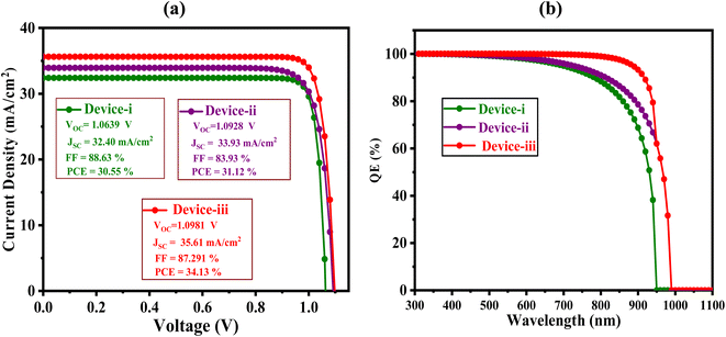 |
| | Fig. 14 (a) J–V and (b) Q–E curves of Device-I, II, and III structures. | |
Table 4 The photovoltaic (PV) metrics obtained in this study with those reported for other double absorber configurations in existing literature (note: E = experimental work and T = theoretical work)
| Structures |
Type of works |
VOC (V) |
FF (%) |
JSC (mA cm−2) |
PCE (%) |
Ref. |
| Device-I |
T |
1.0639 |
88.63 |
32.4022 |
30.55 |
This work |
| Device-II |
T |
1.0928 |
83.93 |
33.9365 |
31.12 |
This work |
| Device-III |
T |
1.0981 |
87.29 |
35.6145 |
34.13 |
This work |
| FTO/SnS2/Sr3SbI3 |
T |
0.93 |
34.67 |
87.31 |
28.05 |
20 |
| FTO/SnS2/Sr3PI3 |
T |
0.92 |
34.65 |
34.65 |
28.15 |
21 |
| CsPbI3/Cs0.25FA0.75PbI3 |
E |
1.20 |
76.00 |
18.91 |
17.39 |
60 |
| CsPbI3/FAPbI3 |
E |
1.22 |
74.00 |
17.26 |
15.60 |
61 |
| MASnI3/MASnBr3 |
T |
1.04 |
78.18 |
31.77 |
25.91 |
62 |
| CsPbI3/CsGeI3 |
T |
1.19 |
86.19 |
23.45 |
24.06 |
63 |
| MASnI3/MAPbI3 |
T |
1.15 |
85.29 |
30.87 |
30.29 |
64 |
| CsPbI3/FAPbI3 |
T |
1.10 |
74.00 |
24.50 |
19.94 |
65 |
| CsPbI3/CsSnI3 |
T |
0.96 |
78.41 |
26.59 |
19.99 |
66 |
4. Plan for experimental validation
Sr3PI3/Sr3SbI3 solar cell technologies should be experimentally evaluated using a comprehensive and multifaceted approach to increase the accuracy of simulation results. This strategy covers material synthesis, device production, characterization, performance analysis, and stability testing. This is a comprehensive plan:
4.1 Synthesis and Preparation of Materials
4.1.1 Production of Sr3PI3 and Sr3SbI3.
4.1.1.1 Chemical procedures. Solid-state synthesis, solution processing, or chemical vapor deposition (CVD) can be used to produce high-purity Sr3PI3 and Sr3SbI3 perovskite materials. Sustain repeatability by following a specified protocol.
4.1.1.2 Characterization. X-ray diffraction (XRD) is used to confirm the crystalline structure and phase purity. Transmission electron microscopy (TEM) and scanning electron microscopy (SEM) are useful for studying morphology and microstructure.
4.1.2 Compositional engineering and doping. To maximize the stability and electrical properties, experiment with different doping levels and compositional modifications. Use energy-dispersive X-ray spectroscopy (EDS) with inductively coupled plasma mass spectrometry (ICP-MS) for precise compositional analysis.
4.2. Manufacturing of devices
4.2.1 Solar cell construction.
4.2.1.1 Layer deposition in the construction of solar cells. Layers can be deposited sequentially using spin-coating, thermal evaporation, or sputtering techniques. Typically, a setup may consist of a metal electrode, Sr3PI3 and Sr3SbI3 active layer, and electron transport layer (ETL).
4.2.1.2 Controlled environment. Manufacture in a glove box with an inert environment to prevent damage from oxygen and moisture.
4.2.2 Quality control. Analyze layer thickness and coverage using profilometry and atomic force microscopy (AFM) to ensure uniformity and durability.
4.3 Evaluation of stability
4.3.1 Stability of the environment. (i) Permit devices to be exposed to ambient conditions (oxygen, humidity), and monitor the gradual decline in device performance over time with recurring I–V measurements.(ii) Conduct accelerated ageing trials at high temperatures and continual illumination to simulate long-term operation conditions.
4.3.2 Mechanical and thermodynamic stability. (i) Perform thermal cycling studies to evaluate the stability in the presence of temperature changes.(ii) Perform mechanical stress testing, if appropriate, to assess the resilience of flexible devices.
4.4 Evaluation by comparison and benchmarking
4.4.1 A reference cells. Create and evaluate reference solar cells utilizing silicon or other perovskites, such as MAPbI3, to act as a performance standard.
4.4.2 Simulation correlation. This is comparing the results of the simulations with the data from the experiment, with special focus to crucial factors like charge carrier lifetimes, PCE, VOC, and JSC. Based on deviations, modify the simulation models.
4.5. More complex characterization methods
4.5.1 Analysis of interface and defects. (i) Use techniques like X-ray photoelectron spectroscopy (XPS) and Fourier-transform infrared spectroscopy (FTIR) to analyze chemical states and interface features.(ii) Examine defects and trap states using deep-level transient spectroscopy (DLTS).
4.5.2 Microscopic methods. (i) Utilizing Kelvin probe force microscopy (KPFM), map the work function and oscillations in the surface potential.(ii) Local electrical characteristics can be examined using conductive AFM, or c-AFM.
By following this detailed approach, it will be possible to validate Sr3PI3/Sr3SbI3 solar cell technologies experimentally and produce high-quality, dependable results that support and enhance simulation predictions, ultimately contributing to the creation of high-performance solar cells.
6. Conclusions
The purpose of this work was to use SCAPS-1D software to model a lead-free heterojunction PSC produced from Sr3PI3/Sr3SbI3. The simulation process for this novel PSC prototype commenced with the creation of the absorber layer, which incorporates two components of perovskites, Sr3PI3/Sr3SbI3, alongside ZnSe as the electron transport layer (ETL) within the SCAPS-1D software environment. The investigation evaluated the effect of absorber layer thicknesses, doping levels, and defect densities, followed by the influence of ETL thickness and doping. Furthermore, utilizing the SCAPS-1D platform, simulations were run to evaluate the impact of temperature, shunt, and series resistance on the electrical properties of this new prototype under standard test conditions (STC). The findings revealed that the maximum simulated efficiency of the new prototype reached 34.1395% with VOC of 1.098137 V, FF of 87.2919%, and JSC of 35.61451 mA cm−2, when the Sr3PI3 thickness was approximately 500 nm and the Sr3SbI3 thickness was around 500 nm. Optimal doping levels were determined to be approximately 1018 cm−3 for Sr3SbI3 and Sr3PI3, with a recommended defect density of around 1012 cm−3 for both absorber layers. Hence, within the production process of this particular PSC, only considerations regarding the absorber layer, FTO, and ETL are crucial for assessing stability and efficiency. Furthermore, it was recommended to maintain the temperature of the fresh PSC prototype at approximately 300 K for optimal performance. For future research directions, experimental investigations are warranted to evaluate the steadiness and longevity of this new device under real-time weather circumstances. Additionally, further studies should explore the effects of different HTL, ETL, and FTO materials on the relationship and performance of this prototype.
Ethical approval
All the authors declare that the manuscript does not have studies on human subjects, human data or tissue, or animals.
Data availability
Data will be made available on reasonable request.
Author contributions
Avijit Ghosh: conceptualization, methodology, software, validation, formal analysis, visualization, investigation, data curation, supervision, writing—original draft, and review and editing. Mohammad Fokhrul Islam Buian, Md. Maniruzzaman, Md Mahfuz Hossain, and Abul Kalam Azad: methodology, software, validation, formal analysis, writing—original draft, and review and editing. Asif Ahammad Miazee, Islam Ragab, Abeer A. Hassan, H. A. Alrafai, and Siham Khalaf Alla Abdelrahim: software, validation, formal analysis, writing—original draft, and review and editing.
Conflicts of interest
The authors have no conflicts of interest.
Acknowledgements
The authors extend their appreciation to the Deanship of Research and Graduate Studies at King Khalid University for funding this work through Large Research Project under grant number RGP2/94/45. The authors also would like to offer their heartfelt appreciation to Dr Marc Burgelman and his colleagues at the EIS Department at the University of Gent in Belgium for providing the opportunity to use the SCAPS-1D software.
References
- N. Kannan and D. Vakeesan, Solar energy for future world: - A review, Renewable Sustainable Energy Rev., 2016, 62, 1092–1105, DOI:10.1016/j.rser.2016.05.022.
- M. F. Rahman, et al., The optical and electronic properties of inorganic halide perovskite Sr3NCl3 under applied biaxial strain, J. Mater. Sci., 2023, 58(32), 13100–13117, DOI:10.1007/s10853-023-08825-5.
- A. Ghosh, et al., Inorganic novel cubic halide perovskite Sr3AsI3: Strain-activated electronic and optical properties, Heliyon, 2023, 9(8), e19271, DOI:10.1016/j.heliyon.2023.e19271.
- M. F. Rahman, et al., An investigation on strain-incited electronic and optical properties of novel inorganic cubic material Sr3AsCl3, J. Solid State Chem., 2023, 328, 124341, DOI:10.1016/j.jssc.2023.124341.
- A. Ghosh, et al., Structural, electronic and optical characteristics of inorganic cubic perovskite Sr 3 AsI 3, Opt. Continuum, 2023, 2(10), 2144, DOI:10.1364/OPTCON.495816.
- M. F. Rahman, et al., Unraveling the strain-induced and spin–orbit coupling effect of novel inorganic halide perovskites of Ca3AsI3 using DFT, AIP Adv., 2023, 13(8) DOI:10.1063/5.0156961.
- M. A. B. Shanto, et al., Investigating how the electronic and optical properties of a novel cubic inorganic halide perovskite, Sr3NI3 are affected by strain, F1000Research, 2023, 12, 1005, DOI:10.12688/f1000research.137044.1.
- A. Ghosh, et al., Strain-induced changes in the electronic, optical and mechanical properties of the inorganic cubic halide perovskite Sr3PBr3 with FP-DFT, J. Phys. Chem. Solids, 2024, 191, 112053, DOI:10.1016/j.jpcs.2024.112053.
- Y.-N. Zhang, B. Li, L. Fu, Y. Zou, Q. Li and L.-W. Yin, Enhanced optical absorption and efficient cascade electron extraction based on energy band alignment double absorbers perovskite solar cells, Sol. Energy Mater. Sol. Cells, 2019, 194, 168–176, DOI:10.1016/j.solmat.2019.02.014.
- T. AlZoubi, A. Moghrabi, M. Moustafa and S. Yasin, Efficiency boost of CZTS solar cells based on double-absorber architecture: Device modeling and analysis, Sol. Energy, 2021, 225, 44–52, DOI:10.1016/j.solener.2021.07.012.
- M. F. Rahman, et al., Design and numerical investigation of cadmium telluride (CdTe) and iron silicide (FeSi2) based double absorber solar cells to enhance power conversion efficiency, AIP Adv., 2022, 12(10), 1–11, DOI:10.1063/5.0108459.
- H. Abedini-Ahangarkola, S. Soleimani-Amiri and S. Gholami Rudi, Modeling and numerical simulation of high efficiency perovskite solar cell with three active layers, Sol. Energy, 2022, 236, 724–732, DOI:10.1016/j.solener.2022.03.055.
- P. Nayak, S. Mahesh, H. Snaith and D. Cahen, Photovoltaic solar cell technologies: analysing the state of the art, Nat. Rev. Mater., 2019, 4, 1, DOI:10.1038/s41578-019-0097-0.
- J. Li, et al., Biological impact of lead from halide perovskites reveals the risk of introducing a safe threshold, Nat. Commun., 2020, 11(Jan) DOI:10.1038/s41467-019-13910-y.
- F. Ünlü, M. Deo, D. S. Mathur, T. Kirchartz and A. Kulkarni, Bismuth-based halide perovskite and perovskite-inspired light absorbing materials for photovoltaics, J. Phys. D Appl. Phys., 2021, 55(Nov) DOI:10.1088/1361-6463/ac3033.
- M. Roknuzzaman, K. Ostrikov, H. Wang, A. Du and T. Tesfamichael, Towards lead-free perovskite photovoltaics and optoelectronics by ab-initio simulations, Sci. Rep., 2017, 7(1), 14025, DOI:10.1038/s41598-017-13172-y.
- M. Emetere, O. Bello and A. Afolalu, Enhancement of novel NaZnBr3 perovskite for solar cells application, Energy Rep., 2022, 8, 4453–4460, DOI:10.1016/j.egyr.2022.03.087.
- M. F. Rahman, et al., Exploring the impact of strain on the electronic and optical properties of inorganic novel cubic perovskite Sr 3 PI 3, Phys. Scr., 2023, 98(11), 115105, DOI:10.1088/1402-4896/acfce9.
- M. S. Islam, et al., Investigation strain effects on the electronic, optical, and output performance of the novel inorganic halide perovskite Sr3SbI3 solar cell, Chin. J. Phys., 2024, 88, 270–286, DOI:10.1016/j.cjph.2024.01.011.
- M. S. Reza, et al., Boosting efficiency above 28% using effective charge transport layer with Sr 3 SbI 3 based novel inorganic perovskite, RSC Adv., 2023, 13(45), 31330–31345, 10.1039/D3RA06137J.
- A. Ghosh, et al., Enhancing solar cell efficiency beyond 27% through the implementation of an efficient charge transport layer utilizing an innovative inorganic perovskite Sr3PI3, J. Phys. Chem. Solids, 2024, 190, 112029, DOI:10.1016/j.jpcs.2024.112029.
- M. Haghighi, M. Minbashi, N. Taghavinia, D.-H. Kim, S. M. Mahdavi and A. A. Kordbacheh, A modeling study on utilizing SnS2 as the buffer layer of CZT(S, Se) solar cells, Sol. Energy, 2018, 167, 165–171, DOI:10.1016/j.solener.2018.04.010.
- W. Chu, X. Li, S. Li, J. Hou, Q. Jiang and J. Yang, High-Performance Flexible Perovskite Solar Cells with a Metal Sulfide Electron Transport Layer of SnS 2 by Room-Temperature Vacuum Deposition, ACS Appl. Energy Mater., 2019, 2(1), 382–388, DOI:10.1021/acsaem.8b01405.
- R. Kumari, M. Mamta, R. Kumar, Y. Singh and V. N. Singh, 24% Efficient, Simple ZnSe/Sb 2 Se 3 Heterojunction Solar Cell: An Analysis of PV Characteristics and Defects, ACS Omega, 2023, 8(1), 1632–1642, DOI:10.1021/acsomega.2c07211.
- A. Ghosh, et al., A theoretical investigation of MoS2-based solar cells with CdS electron transport layer and V2O5 hole transport layer for boosting performance, Mater. Sci. Eng., B, 2024, 307, 117521, DOI:10.1016/j.mseb.2024.117521.
- M. Burgelman, K. Decock, S. Khelifi and A. Abass, Advanced electrical simulation of thin film solar cells, Thin Solid Films, 2013, 535(1), 296–301, DOI:10.1016/j.tsf.2012.10.032.
- M. A. Ashraf and I. Alam, Numerical simulation of CIGS, CISSe and CZTS-based solar cells with In2S3 as buffer layer and Au as back contact using SCAPS 1D, Eng. Res. Express, 2020, 2(3), 35015, DOI:10.1088/2631-8695/abade6.
- L. ∼I. Nykyruy, R. ∼S. Yavorskyi, Z. ∼R. Zapukhlyak, G. Wisz and P. Potera, Evaluation of CdS/CdTe thin film solar cells: SCAPS thickness simulation and analysis of optical properties, Opt. Mater., 2019, 92, 319–329, DOI:10.1016/j.optmat.2019.04.029.
- N. K. Bansal, S. Mishra, H. Dixit, S. Porwal, P. Singh and T. Singh, Machine Learning in Perovskite Solar Cells: Recent Developments and Future Perspectives, Energy Technol., 2023, 11(12), 2300735, DOI:10.1002/ente.202300735.
- K. T. Arockiya-Dass, K. Sekar and L. Marasamy, Theoretical Insights of Degenerate ZrS2 as a New Buffer for Highly Efficient Emerging Thin-Film Solar Cells, Energy Technol., 2023, 11(9), 2300333, DOI:10.1002/ente.202300333.
- G. Kumar, B. K. Ravidas, S. Bhattarai, M. K. Roy and D. P. Samajdar, Exploration of the photovoltaic properties of oxide-based double perovskite Bi2FeCrO6 using an amalgamation of DFT with spin–orbit coupling effect and SCAPS-1D simulation approaches, New J. Chem., 2023, 47(40), 18640–18658, 10.1039/D3NJ02841K.
- S. Gohri, et al., Achieving 24.6% efficiency in 2D perovskite solar cells: Bandgap tuning and MXene contact optimization in (BDA)(MA)n−1PbnI3n+1 structures, Chem. Phys. Lett., 2024, 845, 141291, DOI:10.1016/j.cplett.2024.141291.
- A. Ghosh, A. A. Hassan, H. A. Alrafai and S. K. A. Abdelrahim, A comprehensive study on electron and hole transport layers for designing and optimizing the efficiency of MoSe2-Based solar cells using numerical simulation techniques, Heliyon, 2024, 10(16), e35061, DOI:10.1016/j.heliyon.2024.e35061.
- M. S. Reza, et al., Tuning the Hole Transport Layer in the Ca3SbI3 Absorber-Based Solar Cells to Improve the Power Conversion Efficiency, J. Phys. Chem. Solids, 2024, 112250, DOI:10.1016/j.jpcs.2024.112250.
- A. Ghosh, et al., Improving the power conversion efficiency of RbPbBr3 absorber based solar cells through the variation of efficient hole transport layers, J. Phys. Chem. Solids, 2024, 193, 112179, DOI:10.1016/j.jpcs.2024.112179.
- M. F. I. Buian, et al., A novel investigation into strain-induced changes in the physical properties and solar cell performances of lead-free Ca3NCl3 perovskite, Mater. Sci. Semicond. Process., 2024, 180, 108580, DOI:10.1016/j.mssp.2024.108580.
- M. F. Rahman, et al., First-principles analysis of how Cobalt doping affects the structural, electronic, and optical properties of α-MoO3, Indian J. Phys., 2023 DOI:10.1007/s12648-023-03043-w.
- A. A. Hassan, et al., Investigating the physical characteristics and photovoltaic performance of inorganic Ba3NCl3 perovskite utilizing DFT and SCAPS-1D simulations, Mater. Sci. Eng., B, 2024, 308, 117559, DOI:10.1016/j.mseb.2024.117559.
- A. Ghosh, et al., Investigating of novel inorganic cubic perovskites of A3BX3 (A=Ca, Sr, B P, As, X=I, Br) and their photovoltaic performance with efficiency over 28, J. Alloys Compd., 2024, 986, 174097, DOI:10.1016/j.jallcom.2024.174097.
- M. S. Reza, et al., Design and Optimization of High-Performance Novel RbPbBr 3 -Based Solar Cells with Wide-Band-Gap S-Chalcogenide Electron Transport Layers (ETLs), ACS Omega, 2024 DOI:10.1021/acsomega.3c08285.
- N. Jahan, et al., A comparative study of CuO based solar cell with ZnTe HTL and SnS2 ETL using SCAPS 1D simulation, J. Optom., 2024 DOI:10.1007/s12596-024-01800-6.
- R. Jeyakumar, A. Bag, R. Nekovei and R. Radhakrishnan, Influence of Electron Transport Layer (TiO2) Thickness and Its Doping Density on the Performance of CH3NH3PbI3-Based Planar Perovskite Solar Cells, J. Electron. Mater., 2020, 49(6), 3533–3539, DOI:10.1007/s11664-020-08041-w.
- J. Cerdà, J. Arbiol, R. Diaz, G. Dezanneau and J. Morante, Synthesis of perovskite-type BaSnO3 particles obtained by a new simple wet chemical route based on a sol–gel process, Mater. Lett., 2002, 56(3), 131–136, DOI:10.1016/S0167-577X(02)00428-7.
- Z. Gu, et al., Novel planar heterostructure perovskite solar cells with CdS nanorods array as electron transport layer, Sol. Energy Mater. Sol. Cells, 2015, 140, 396–404, DOI:10.1016/j.solmat.2015.04.015.
- M. Burgelman, J. Verschraegen, S. Degrave and P. Nollet, Modeling thin-film PV devices, Prog. Photovolt.: Res. Appl., 2004, 12(23), 143–153, DOI:10.1002/pip.524.
- C. Chen, et al., Characterization of basic physical properties of Sb2Se3 and its relevance for photovoltaics, Front. Optoelectron, 2017, 10(1), 18–30, DOI:10.1007/s12200-017-0702-z.
- Y. H. Khattak, F. Baig, H. Toura, S. Beg and B. M. Soucase, Efficiency enhancement of Cu2BaSnS4 experimental thin-film solar cell by device modeling, J. Mater. Sci., 2019, 54(24), 14787–14796, DOI:10.1007/s10853-019-03942-6.
- H. Zhang, S. Cheng, J. Yu, H. Zhou and H. Jia, Prospects of Zn(O,S) as an alternative buffer layer for Cu 2 ZnSnS 4 thin-film solar cells from numerical simulation, Micro Nano Lett., 2016, 11(7), 386–390, DOI:10.1049/mnl.2016.0130.
- A. Ghosh, et al., Solar power conversion: CuI hole transport layer and Ba 3 NCl 3 absorber enable advanced solar cell technology boosting efficiency over 30, RSC Adv., 2024, 14(33), 24066–24081, 10.1039/D4RA03695F.
- Y. Zhou and A. Gray-Weale, A numerical model for charge transport and energy conversion of perovskite solar cells, Phys. Chem. Chem. Phys., 2016, 18(6), 4476–4486, 10.1039/C5CP05371D.
- O. Ahmad, A. Rashid, M. W. Ahmed, M. F. Nasir and I. Qasim, Performance evaluation of Au/p-CdTe/Cs2TiI6/n-TiO2/ITO solar cell using SCAPS-1D, Opt. Mater., 2021, 117, 111105, DOI:10.1016/j.optmat.2021.111105.
- H. Heriche, Z. Rouabah and N. Bouarissa, New ultra thin CIGS structure solar cells using SCAPS simulation program, Int. J. Hydrogen Energy, 2017, 42(15), 9524–9532, DOI:10.1016/j.ijhydene.2017.02.099.
- E. Karimi and S. M. B. Ghorashi, Simulation of perovskite solar cell with P 3 HT hole-transporting materials, J. Nanophotonics, 2017, 11(3), 032510, DOI:10.1117/1.JNP.11.032510.
- F. Behrouznejad, S. Shahbazi, N. Taghavinia, H.-P. Wu and E. Wei-Guang Diau, A study on utilizing different metals as the back contact of CH 3 NH 3 PbI 3 perovskite solar cells, J. Mater. Chem. A, 2016, 4(35), 13488–13498, 10.1039/C6TA05938D.
- M. F. Hossain, et al., Design and simulation numerically with performance enhancement of extremely efficient Sb2Se3-Based solar cell with V2O5 as the hole transport layer, using SCAPS-1D simulation program, Opt. Commun., 2024, 559, 130410, DOI:10.1016/j.optcom.2024.130410.
- M. S. Reza, et al., New highly efficient perovskite solar cell with power conversion efficiency of 31% based on Ca3NI3 and an effective charge transport layer, Opt. Commun., 2024, 561, 130511, DOI:10.1016/j.optcom.2024.130511.
- M. A. Rahman, et al., Impact of A-Cations Modified on the Structural, Electronic, Optical, Mechanical, and Solar Cell Performance of Inorganic
Novel A 3 NCl 3 (A = Ba, Sr, and Ca) Perovskites, Energy Fuels, 2024 DOI:10.1021/acs.energyfuels.4c00525.
- M. S. Islam, et al., An in-depth analysis of how strain impacts the electronic, optical, and output performance of the Ca3NI3 novel inorganic halide perovskite, J. Phys. Chem. Solids, 2024, 185, 111791, DOI:10.1016/j.jpcs.2023.111791.
- P. Khan, T. Mahmood, K. Ayub, S. Tabassum and M. Amjad Gilani, Turning diamondoids into nonlinear optical materials by alkali metal Substitution: A DFT investigation, Opt. Laser Technol., 2021, 142, 107231–Oct, DOI:10.1016/j.optlastec.2021.107231.
- Q. Zhao, et al., High efficiency perovskite quantum dot solar cells with charge separating heterostructure, Nat. Commun., 2019, 10(1), 2842, DOI:10.1038/s41467-019-10856-z.
- F. Li, et al., Perovskite Quantum Dot Solar Cells with 15.6% Efficiency and Improved Stability Enabled by an α-CsPbI 3/FAPbI 3 Bilayer Structure, ACS Energy Lett., 2019, 4(11), 2571–2578, DOI:10.1021/acsenergylett.9b01920.
- U. Mandadapu, S. V. Vedanayakam, K. Thyagarajan and B. J. Babu, Optimisation of high efficiency tin halide perovskite solar cells using SCAPS-1D, Int. J. Simul. Process Model, 2018, 13(3), 221, DOI:10.1504/IJSPM.2018.093097.
- X. Li, et al., Theoretical analysis of all-inorganic solar cells based on numerical simulation of CsGeI3/CsPbI3 with p-p+ built-in electric field, Sol. Energy, 2022, 247, 315–329, DOI:10.1016/j.solener.2022.10.039.
- B. Farhadi, M. Ciprian, F. Zabihi and A. Liu, Influence of contact electrode and light power on the efficiency of tandem perovskite solar cell: Numerical simulation, Sol. Energy, 2021, 226, 161–172, DOI:10.1016/j.solener.2021.08.043.
- A. Hajjiah, M. Gamal, I. Kandas, N. E. Gorji and N. Shehata, DFT and AMPS-1D simulation analysis of all-perovskite solar cells based on CsPbI3/FAPbI3 bilayer structure, Sol. Energy Mater. Sol. Cells, 2022, 248, 112026, DOI:10.1016/j.solmat.2022.112026.
- C. Ming, et al., The design and performance optimization of all-inorganic CsPbIBr2/CsSnI3 heterojunction perovskite solar cells, Sol. Energy, 2023, 263, 111885, DOI:10.1016/j.solener.2023.111885.
|
| This journal is © The Royal Society of Chemistry 2024 |
Click here to see how this site uses Cookies. View our privacy policy here. 
 Open Access Article
 This Open Access Article is licensed under a Creative Commons Attribution-Non Commercial 3.0 Unported Licence
 *a,
Mohammad Fokhrul Islam Buianb,
Md. Maniruzzamancd,
Md. Mahfuz Hossaine,
Abul Kalam Azadf,
Asif Ahammad Miazeeg,
Islam Ragabh,
Abeer A. Hassani,
H. A. Alrafaii and
Siham Khalaf Alla Abdelrahimi
*a,
Mohammad Fokhrul Islam Buianb,
Md. Maniruzzamancd,
Md. Mahfuz Hossaine,
Abul Kalam Azadf,
Asif Ahammad Miazeeg,
Islam Ragabh,
Abeer A. Hassani,
H. A. Alrafaii and
Siham Khalaf Alla Abdelrahimi