
 Open Access Article
 This Open Access Article is licensed under a Creative Commons Attribution-Non Commercial 3.0 Unported Licence
The impact of processing voltage of wire electric discharge machining on the performance of Mo doped V–VO0.2 based Archimedean micro-supercapacitors†
Ri Chen a,
Jie Qina,
Zehan Xua,
Siqi Lva,
Zhenhao Taoa,
Jiale Hea,
Peipei Zhou*a,
Zhaoyu Shu*a,
Zhixin Zhuang*b,
Wenxia Wangc,
Yunying Xud,
Lanying Xua,
Cheng Denga,
Igor Zhitomirskye and
Kaiyuan Shif
a,
Jie Qina,
Zehan Xua,
Siqi Lva,
Zhenhao Taoa,
Jiale Hea,
Peipei Zhou*a,
Zhaoyu Shu*a,
Zhixin Zhuang*b,
Wenxia Wangc,
Yunying Xud,
Lanying Xua,
Cheng Denga,
Igor Zhitomirskye and
Kaiyuan Shif
aDepartment of Mechatronic Engineering, Guangdong Polytechnic Normal University, Guangzhou, 510665, China. E-mail: zhoupp@gpnu.edu.cn; soshelp8888@163.com
bSchool of Electrical Engineering, Xinjiang Railway Vocational and Technical College, Hami, Xinjiang 839000, China. E-mail: 861401232@qq.com
cDepartment of Biomedical and Pharmaceutical Sciences, Guangdong University of Technology, Guangzhou, 510006, PR China
dSchool of Education, Guangdong Polytechnic Normal University, Guangzhou, 510665, PR China
eDepartment of Materials Science and Engineering, McMaster University, Hamilton, L8S 4L7, Canada
fDepartment of Materials Science and Engineering, Sun Yat-Sen University, Guangzhou, 510275, PR China
First published on 6th September 2024
Abstract
Vanadium oxide-based electrode materials have attracted increasing attention owing to their extraordinary capacitance and prolonged lifespan, excellent conductivity and outstanding electrochemical reversibility. However, the development of vanadium oxide-based integrated electrodes with outstanding capacitive performance is an enduring challenge. This research reports a facile method for structuring 3D Archimedean micro-supercapacitors (AMSCs) composed of Mo doped V–VO0.2 (Mo@V–VO0.2) based integrated electrodes with designable geometric shape, using computer-aided wire electric discharge machining (WEDM). The performance of Mo@V–VO0.2 based AMSCs manufactured by different processing voltages of 60 V, 80 V and 100 V were evaluated. It was found that 80 V is the optimal processing voltage for manufacturing Mo@V–VO0.2 based AMSCs with the best electrochemical performance. This device demonstrates superior capacitive behavior even at an ultra-high scan rate of 50, 000 mV s−1, and achieves a good capacitance retention rate of 94.4% after 2000 cycles. Additionally, the characteristics of electric field distribution were also simulated for optimizing the geometric structure of the microdevices. This WEDM fabrication technique, which is easy, secure, patternable, efficient, economical, eco-friendly, and does not require binders or conductive additives, enables the development of high-capacity 3D pseudocapacitive micro-supercapacitors and demonstrates the great potential for metal oxide synthesis and microdevice manufacturing.
1. Introduction
With the prevalent utilization of microscale electronic devices, miniaturization and integration technologies have become a critical focus.1 Currently, significant advancements have been achieved in microscale electronic devices such as portable, wearable sensors and flexible displays, but the development of energy storage devices has lagged behind other electronic devices. Furthermore, a compelling demand exists for downsizing energy storage devices in sectors like healthcare and aviation.2 Consequently, the spotlight has turned to micro-supercapacitors (MSCs) and micro-batteries with small sizes, easy integration, and high energy storage capacity.3,4 However, the present micro-batteries are hindered by their slow charging rates and short operational lifespan, which leads to frequent replacements after hundreds to thousands of recharging cycles.5,6 In contrast to micro-batteries, MSCs exhibit an extended lifecycle, capable of enduring thousands or more charge–discharge cycles, which can effectively reduce the frequency of replacements.7 Furthermore, MSCs have exceedingly rapid charge and discharge rates, which enable them to efficiently accumulate and discharge significant electrical energy in a short time. Moreover, MSCs are environmentally friendly due to their extended lifespan and infrequent replacement requirements.8–10 Additionally, the membrane-free structure design of MSCs facilitates high-efficiency ion diffusion and effectively prevents the occurrence of a short-circuit.11 Therefore, due to the above advantages, MSCs have received a lot of attention and are popular in terms of energy storage. Carbon based MSCs attract researchers' attention because of their fast charging/discharging rate, long cycling life and good flexibility.12 In contrast to carbon based MSCs, pseudocapacitive micro-supercapacitors (PC-MSCs) demonstrate a substantially higher specific capacitance. This is because the capacitance of the carbon based MSCs is derived from the accumulation of charge at the electrode/electrolyte interface, while PC-MSCs achieve a superior electrical capacity through the rapid and reversible redox reaction occurring at the electrode.13At present, a variety of fabrication methods, including conventional photolithography,14,15 screen printing,16 inkjet printing,17 3D printing,18 stamping,19 laser direct writing,20 plasma etching,21 and mask-assisted filtering,22 have been developed for the production of planar MSCs. Unfortunately, the current manufacturing methods have suffered from obvious constraints in manufacturing of MSCs. For instance, the template or photoresist utilizing in traditional photolithography must be removed using a buffer solution and extreme high temperature exposure is also involved in the device processing procedures.23 These will lead to a decrease in the fabricated efficiency and the performance of MSCs.24 Screen printing often results in uneven ink coating on the substrate, which greatly affects the capacitive behavior of the whole device. In addition, the preparation of the patterning silk screen will inevitably raise production expenses, especially in large-scale production.16,25 Moreover, since 3D printing is a process of layer-by-layer construction, the surface of the manufactured capacitor may have roughness, burrs or other surface defects, which may affect the performance and stability of the capacitor. Furthermore, the limited materials currently available for 3D printing inks restrict the further development of MSCs with customized capacitive performance.26 Moreover, low conducting binders was normally used for ink processing, which inevitably results in poor conductivity of the devices, especially at high charging/discharging rates. Recently, laser manufacturing technique has been developed for manufacturing MSCs, but it necessitates costly machinery with precision management and accurate operational control, which requires high standards from the manufacturing process. Additionally, laser manufacturing may result in material localized heating, which can cause thermal stress problems and impact the effectiveness and stability of the MSCs. Furthermore, conventional laser-processed materials, such as carbon-based materials and graphene, often result in low capacitance for MSCs.27–29 Aim to enhance the capacitance, various laser processing techniques have been explored to manufacture different PC-MSCs. For instance, Liu et al.30 investigated a flexible in-plane hybrid MSCs based on Fe3O4 nanoparticles anchored porous laser-induced graphene. This investigation proved that Fe3O4 based PC-MSCs showed more than 100 times higher specific capacitance than that of graphene based MSCs.
There has been a growing interest in the fabrication of high performance PC-MSCs with various active materials, encompassing polypyrrole (PPy),31–33 polyaniline (PANI),34 poly(3,4-ethylenedioxythiophene) (PEDOT),35 FeOOH,36 Cu(OH)2,37 Fe3O4,38 Mn3O4,39 NiFe2O4,40 RuO2,41 NiCo2S4,42 MoS2,43 and MXene.44,45 Transition metal oxides are often utilized as electrode materials for supercapacitors because of their higher specific capacitance and better cyclic stability compared to most conductive polymers.46 Vanadium oxides distinguish themselves from most transition metal oxides by offering access to four readily interconvertible valence states (II–V). Vanadium oxides based materials are recognized as advanced active materials for strong power electrochemical capacitors owing to their extraordinary capacitance and prolonged lifespan, excellent conductivity and outstanding electrochemical reversibility.47,48 For example, Zhang et al.49 developed a simple laser ablation method for preparing VOx/reduced graphene oxide (rGO) composites with hierarchical structures. Minyawi et al.50 fabricated a stable ink for screen printing, using a non-poisonous solvent and vanadium dioxide (VO2). The performance was further improved by hybridization with gold nanoparticles. Zhou et al.51 fabricated V2O5 based MSCs with ordered porous layered structure and uniform electric field intensity by combining various strategies, such as micro-ultrasonic, vacuum filtration and 3D printing technology. Moreover, Zhou et al.52 prepared a high-performance composite 3D printing inks by adopting NiCo-metal–organic frameworks (MOFs)@CoOOH@V2O5 as active materials, and using carbon nanotubes and graphene oxide for adjusting their electronic conductivity and rheology behavior. Although researchers achieved enhanced capacitive performance of vanadium oxide based electrode materials and devices, the aforementioned complex processes for manufacturing PC-MSCs require costly materials, extra conductive media, toxic chemicals, and extra current collectors, inevitably resulting in high manufacturing expenses and low production efficiency.53 Furthermore, their areal capacitances are still significantly below the required levels for commercial application. Recently, an increasing research interest have been focused on the development of 3D conductive network, such as 3D carbon network and 3D MXene-MOFs, for tailoring the physical or chemical properties of various composite materials.54–56 In order to boost their areal capacitances, researchers have developed a variety of 3D current collectors for PC-MSCs, which play a crucial role in enhancing electron transfer and facilitating the fast diffusion of electrolyte ions.37,57 For instance, Liu et al.45 grew MXene on 3D MOFs to prepare 3D MXene-MOFs composites to boost the electrochemical performance of supercapacitors. It was found that 3D MOFs could effectively prevented the aggregation of MXene, which is beneficial for promoting electrolyte access and improving conductivity. Xie et al.58 adopted laser engraving to fabricate 3D interdigitated Ni foams current collectors for electrodeposition of MnO2 and PPy pseudocapacitive materials for PC-MSCs. Jiang et al.59 fabricated 3D Nickel foam interdigitated current collectors using laser machining. Subsequently, NiCo2S4 based interdigitated positive electrode and carbon nanofiber based interdigitated negative electrode were prepared by hydrothermal synthesis and chemical vapor deposition strategy, respectively for constructing NiCo2S4/carbon nanofiber hybrid devices. Their results indicated that the areal capacitance, cyclic stability and rate performance of the fabricated PC-MSCs have been improved remarkably. This is because 3D electrode configuration design offers many merits, including preparation of electrode materials with good electronic conductivity, high surface area, good structural stability and shortened electron/ion diffusion length, which facilitated fast ion and electron transport. However, the processes involved in fabricating 3D PC-MSCs are multifaceted and require numerous complex procedures, resulting in an unavoidable increase in production cost. Therefore, there is an urgent need for manufacturing high electrochemical performance 3D PC-MSCs with a simple, environmental-friendly and efficient technology, which is free from binders, surfactants, conductive additives, and templates.
Wire electrical discharge machining (WEDM) is a non-traditional machining technique using spark erosion effect to fabricate workpiece with various hardness and complex 3D structures for various applications, such as aerospace, automobiles, atomic reactors and PC-MSCs.60–63 WEDM could fabricate PC-MSCs electrodes with complex geometries at one step without using any aids of chemicals, surfactants, binders, gases, conductive additives, additional current collectors and templates. Moreover, this single step WEDM manufacturing strategy greatly simplifies the fabricated procedures of microelectrodes as it does not require the assistance of additional processes, such as annealing, dispersing, filtering, vacuuming, gas-supplying, centrifugation and ultrasonication. It has been reported that the processing voltage of WEDM showed great influence on the surface morphologies of the machining substrates.64 However, up to now, there is a lack of research investigating on the effect of WEDM processing voltage on the electrochemical performance of PC-MSCs. Therefore, this investigation aims to elucidate the relationship between machining voltages and the electrochemical properties of PC-MSCs fabricated by the specific technique of WEDM. In this context, we developed a single step WEDM to fabricate 3D Mo@V–VO0.2 based PC-MSCs with customized patterns. During WEDM processing, computer-aided manufacturing is utilized to shape a vanadium metal plate into a 3D current collector with Archimedean patterns. At the same time, the elevated temperatures generated within the discharge channels trigger oxidation and Mo doping on the surface of these 3D vanadium current collectors to form 3D Mo@V–VO0.2 integrated electrodes and devices. Another important finding is that the performance of the 3D Mo@V–VO0.2 based PC-MSCs could be tailored by the processing voltage of WEDM. It was found that 80 V is the optimal processing voltage for manufacturing Archimedean micro-supercapacitors (AMSCs) with the best electrochemical performance. This device demonstrates superior capacitance even at an ultra-high scan rate of 50, 000 mV s−1, and maintains a good capacitance retention rate of 94.4% after 2000 cycles. It is important to note that these devices were manufactured without the expensive machinery, manufacturing conditions, toxic or costly materials, or convoluted fabrication processes. Consequently, the production of these 3D Mo@V–VO0.2 based PC-MSCs can streamlined into a straightforward one-step process, eliminating the need for low conductive binders, surface modified agents, extra current collectors and high conductivity additives.
2. Experimental procedures
2.1 Materials
Vanadium metal sheet (V-MS) was supported by the company of Qinghelisheng Metal Materials. The high efficiency WEDM Mo wire was supported by Jinduicheng Molybdenum Mining Guangming Corporation. The KOH solutions were supported by Kell Chemical Technology Company.2.2 Preparation of Mo@V–VO0.2 based electrodes and PC-MSCs
Mo@V–VO0.2 based integrated electrodes were prepared using V-MS as starting material by computer-controlled WEDM method, and then the integrated electrodes were cut into 3D Mo@V–VO0.2 based integrated devices using the same technology. The device was fabricated in deionized water and processed at three different processing voltages of 60 V, 80 V and 100 V, respectively.2.3 Materials and electrochemical characterization
TESCAN MIRA LMS scanning electron microscope (SEM) was adopted to analyze the surface morphology. For electrode material characterization, X-ray photoelectron spectroscopy (XPS) testing was performed by a thermal science K-Alpha instrument. The V–VO0.2 integrated electrode was subjected to X-ray diffraction (XRD) analysis using a Rigaku KαKα diffractometer at a scan rate of 2° min−1. Transmission Electron Microscope (TEM) was performed using Thermo Fisher Helio Nanolab G3 UC instrument. Energy Dispersive X-Ray Spectroscopy (EDX) was performed with Thermo Fisher Talos F200s equipment to analyze the element distribution of electrode material. The oxygen vacancies of electrode material was investigated by Electron Paramagnetic Resonance (EPR) using Bruker EMXplus-6/1 instrument. Cyclic voltammetry (CV) and galvanostatic charge–discharge (GCD) studies were performed using a CHI 660E electrochemical workstation. The CV experiments were studied at scanning rates ranging from 1 to 50![[thin space (1/6-em)]](https://www.rsc.org/images/entities/char_2009.gif) 000 mV s−1, within a potential window of 0–0.6 V. The GCD examination was conducted within a current density range of 0.2–2 mA cm−2 at a testing potential range of 0–0.6 V. The capacitive properties of single PC-MSCs in KOH electrolyte with a concentration of 1 M were analyzed by CV and GCD. The testing area of all the devices is equal to 1 cm2.
000 mV s−1, within a potential window of 0–0.6 V. The GCD examination was conducted within a current density range of 0.2–2 mA cm−2 at a testing potential range of 0–0.6 V. The capacitive properties of single PC-MSCs in KOH electrolyte with a concentration of 1 M were analyzed by CV and GCD. The testing area of all the devices is equal to 1 cm2.
3. Results and discussion
Fig. 1 shows the efficient fabricating process of Mo@V–VO0.2 based integrative PC-MSCs using WEDM technique. The Mo doped VO0.2 active material grown from V-MS and Mo cutting wire is used for energy storage. Fig. 1a shows the untreated V-MS under the support of the jig and fixture. Subsequently, the surface of the V-MS was synchronously oxidized and doped with Mo by the treatment of WEDW (Fig. 1b). Fig. 1c shows the locally amplified WEDM discharge channel diagram between the V-MS and Mo cutting wire experiencing high temperature oxidation and element doping to form Mo doped VO0.2 active material. Thereby, the treated Mo@V–VO0.2 based integrated electrode is cut directly into a Mo@V–VO0.2 based PC-MSCs device with a specified 3D pattern via WEDM with computer-aided control system (Fig. 1d–f). The microdevices with one-trip Archimedean shape (60AMSCs1), two-trips Archimedean shape (60AMSCs2) and three-trips Archimedean shape (60AMSCs3) were prepared by one-step WEDM technique, respectively (Fig. 1g–i). It's important to highlight that WEDM, which benefits from a computer-aided manufacturing process, offers the merits of simplicity, safety, and cost-effectiveness. Moreover, according to the pre-set processing program of the computer, the surface morphology of Mo@V–VO0.2 based integrated electrodes and geometric shape of the microdevices could also be controlled automatically. Moreover, the whole manufacturing process eliminates the usage of dangerous chemicals and toxic solvents, which is very beneficial for environment protection. | ||
| Fig. 1 (a) Untreated V-MS and (b) V-MS during WEDM and (c) enlarged electric discharge channel for generating Mo doped VO0.2 particles during WEDM and (d–i) manufacturing process of Mo doped VO0.2 PC-MSCs devices with different modes. | ||
Morphological characteristics of the Mo@V–VO0.2 electrodes were examined using SEM characterization. The surface morphology of V-MS before processing by WEDM is smooth without any microstructure features (Fig. 2a). Fig. 2b–d shows the images of Mo@V–VO0.2 integrated electrodes treated at different applied voltages of WEDM. At a processing voltage of 60 V, the Mo@VO0.2 particles are sparse, whereas at 100 V they grow larger and show severe agglomeration. Compared to 60 V and 100 V, the surface morphology of the Mo@VO0.2 particles fabricated at 80 V is relatively dense and uniform, which is beneficial for energy storage. Fig. 3a shows the XRD patterns of V-MS without WEDM treatment and with the WEDM cutting treatment carried out at processing voltages of 60, 80 and 100 V, respectively. The XRD pattern of raw V-MS revealed diffraction peaks located at 42.1°, 61.2° and 76.8°, which can be indexed to V, corresponding to the (110), (200) and (211) crystal planes, respectively.65 The XRD patterns of V-MS treated by processing voltages of 60, 80 and 100 V showed similar broad diffraction peaks corresponding to the PDF #10-0321. These diffraction peaks positioned at 40.1°, 43.0°, 62.4° and 76.8° correspond to VO0.2 indexing to the crystal planes of (101), (110), (200) and (211), respectively. But the material also contained amorphous phase, indicating relatively low crystallized of VO0.2 was obtained. This phenomenon was also confirmed by the selected area electron diffraction (SAED) pattern achieved by TEM examination (Fig. 1S†). Fig. 3b displays the high-resolution V 2p spectrum obtained from XPS analysis of a Mo@V–VO0.2 electrode prepared by the WEDM. The XPS spectra were calibrated using C 1s at 284.8 eV as the reference peak. The peaks observed at 512.6 and 513.6 eV can be attributed to metallic vanadium and V2+ oxidation state, respectively.66 Moreover, the broad V 2p3/2 standard peak at 515.0, 516.5, and 517.9 eV is deconvoluted into three distinct peaks, corresponding to the binding energy of V 2p3/2 electrons in the V3+, V4+, and V5+ oxidation states, respectively.67 Moreover, the energy-dispersive X-ray spectroscopy (EDS) element mapping operated with SEM proved that the elements of Mo, V and O are uniformly distributed on the surface of Mo@V–VO0.2 (Fig. 2S†). This uniform element distribution phenomenon was also confirmed by EDX carried out with TEM testing (Fig. 1S†). The multiple valence state of vanadium oxide with Mo doping facilitates fast electronic transportation, which could greatly boost their electrochemical performance. Fig. 3c shows the O 1s spectrum, which can be deconvolved into three standard peaks positioned at 530.2, 531.6, and 532.9 eV, which correspond to metal–O bond, O vacancies, and surface adsorbed water, respectively.68–70 The generated oxygen vacancies were also proved by EPR testing (Fig. 3S†). The sample of 80AMSCs3 showed a g-value of 2.0058, closing to that of a free electron (2.0023), which indicated the appearance of unpaired electrons.71,72 The introduction of oxygen vacancies in VO0.2 is beneficial for accelerating its electronic transportation speed and enhancing its electrochemical performance.
 | ||
| Fig. 2 SEM images of V-MS (a) before vanadium plate processing and integrated electrode at different processing voltages (b) 60 V; (c) 80 V; (d) 100 V. | ||
 | ||
| Fig. 3 (a) XRD profiles, and XPS spectra of (b) V 2p and (c) O 1s, for V-MS after WEDM. | ||
CV tests were performed on 3D PC-MSCs devices with different patterns (60AMSCs1, 60AMSCs2 and 60AMSCs3) fabricated by the same processing voltage of 60 V. Fig. 4a–c show the CV profiles of 60AMSCs1, 60AMSCs2, and 60AMSCs3 devices, respectively. All the obtained CV curves display nearly rectangle shapes, indicating excellent capacitive performance of PC-MSCs devices fabricated via WEDM. The areal capacitances of 60AMSCs1, 60AMSCs2, and 60AMSCs3, derived from their respective CV profiles, are illustrated in Fig. 4d. It demonstrates that 60AMSCs3 obtains a higher capacitance of 16.8 mF cm−2 (1 mV s−1) than that of 60AMSCs1 and 60AMSCs2. The same occurrence was noted at other scanning rates for 60AMSCs1, 60AMSCs2, and 60AMSCs3. This is mainly attributed to the reduction of electrode width which is beneficial for accelerating the ion transport rate. This phenomenon is further proved by the simulations of the electric potential distribution and electric field intensity distribution for 60AMSCs1, 60AMSCs2, and 60AMSCs3 respectively (Fig. 4S†).
 | ||
| Fig. 4 CVs for (a) 60AMSCs1, (b) 60AMSCs2, (c) 60AMSCs3 at 1–100 mV s−1 and (d) corresponding capacitance derived from CV profiles. | ||
To explore the capacitive behavior of 60AMSCs1, 60AMSCs2, and 60AMSCs3 devices at ultra-high scan rates, CV testings were conducted from 10 to 50 V s−1 (Fig. 5a–c). The shapes of the CV curve sustained as nearly rectangle, which confirmed the excellent capacitive performance of 3D PC-MSCs devices fabricated through WEDM. This excellent electrochemical performance is due to the 3D binder-free integrated electrode design, Mo doping and multivalent states of vanadium oxide, which enhanced the electrical conductivity of the electrodes and fastened the ion and electron transport. In Fig. 5d, the areal capacitances of devices 60AMSCs1, 60AMSCs2, and 60AMSCs3 are presented, calculated based on their respective CV profiles. Compared to 60AMSCs1 and 60AMSCs2, 60AMSCs3 achieved lager capacitance at the same scan rate, which was consistent with those acquired at 1–100 mV s−1 (Fig. 4), benefiting from the shorten average ions diffusion distance between adjacent electrodes by the reduction of electrode width. Even at 50 V s−1, the areal capacitance of 60AMSCs3 remained at 2.7 mF cm−2. This is a benefit from the 3D binder-free integrated electrode design, Mo doping, introduction of oxygen vacancies and multivalent states of vanadium oxide, which enhanced the electronic conductivity of vanadium oxide active material and promoted the ion and electron transport efficiency. Fig. 6a displays the GCD profiles of 60AMSCs1, 60AMSCs2, and 60AMSCs3 devices at 0.9 mA cm−2. The symmetrical triangles of all GCD profiles indicate that good capacitive properties were achieved. Compared to 60AMSCs1 and 60AMSCs2, 60AMSCs3 obtained higher capacitance, which is consistent with the CV examination results shown in Fig. 4 and 5. As shown in Fig. 6b, the areal capacitance values of 60AMSCs3 devices decreased slightly with the increase of the testing current densities from 0.3 to 2 mA cm−2 and obtained a good capacity retention of 82.5%.
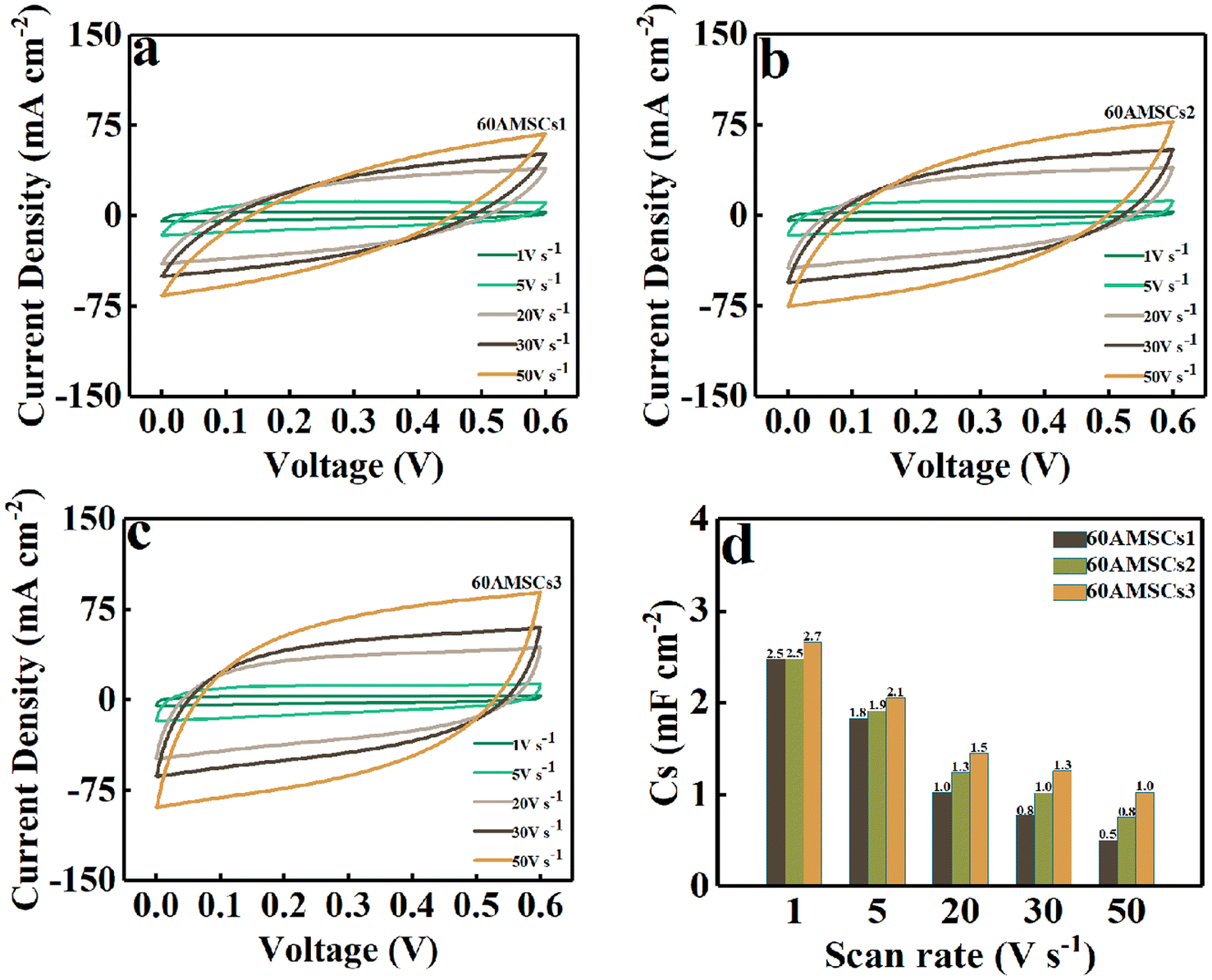 | ||
| Fig. 5 CVs for (a) 60AMSCs1, (b) 60AMSCs2, (c) 60AMSCs3 at 1–50 V s−1 and (d) corresponding capacitance derived from CV profiles. | ||
 | ||
| Fig. 6 (a) The GCD images of 60AMSCs1, 60AMSCs2 and 60AMSCs3, (b) corresponding capacitance derived from GCD profiles for 60AMSCs3. | ||
In order to further demonstrate the advantages of WEDM technology in manufacturing 3D Mo@V–VO0.2 integrated electrode with controllable surface morphology, the Mo@V–VO0.2 based AMSCs3 were manufactured with different WEDM processing voltages (60 V, 70 V, 80 V, 90 V and 100 V), which were named as 60AMSCs3, 70AMSCs3, 80AMSCs3, 90AMSCs3 and 100AMSCs3 respectively. Fig. 7a–c shows the CV curves of 60AMSCs3, 80AMSCs3, and 100AMSCs3 devices at low scan rates from 1 to 100 mV s−1. The box shape CV profiles indicate that Mo@V–VO0.2 based PC-MSCs fabricated via WEDM have excellent capacitive properties. Fig. 7d showed the areal capacitance of 60AMSCs3, 80AMSCs3, and 100AMSCs3 derived from CV. It is evident that the 80AMSCs3 device achieved the highest capacitance value of 25.2 mF cm−2 (at 1 mV s−1) among these three microdevices. The 80AMSCs3 prepared by processing voltage of 80 V also showed the best capacity among these three devices at other different scan rates. This is because the Mo@VO0.2 particles prepared by the processing voltage of 80 V are dense and uniform, providing more active sites for energy storage and thus enhance its electrochemical performance. Moreover, the obtained capacity of 80AMSCs3 is higher than that of 70AMSCs3, 90AMSCs3 (Fig. 5S†), PANI/V2O5 based PC-MSCs fabricated by combined processes of electrodeposition, spray coating, solvothermal method, centrifugation, pyrolysis, annealing and dispersing,73 rGO/V2O5 based PC-MSCs fabricated by compound procedures of spray coating, sputtering, modified Hummer's method, annealing, stirring, filtering and ultrasonication,74 Graphene–PEDOT–poly(styrene sulfonic acid) (PSS) based PC-MSCs fabricated by complex processes of mask-assisted spray deposition, electrochemically exfoliating, stirring, heating and sonication,75 MXene based MSCs prepared by combined processes of laser machining, spray coating, etching, stirring, filtering and centrifugation,76 carbon nanotubes (CNT) based MSCs manufactured with a combination processes of spin coating, photolithography, ultrasonication, stirring, centrifugation, drying, pyrolysis and baking,77 activated carbon prepared by combined processes of inkjet printing, photolithography, chemical vapour deposition, evaporation and etching,78 carbon onions based MSCs fabricated by complex processes of electrophoretic deposition, photolithography, etching, thermal growing, annealing and heating,79 graphene based MSCs fabricated by complex processes of spin coating, lithography, O2 plasma treatment, and CH4 plasma treatment,80 graphene based MSCs fabricated by complex processes of laser-scribing, modified Hummer's method, stirring, and drop-cast,81 and rGO based MSCs prepared by complex processes of laser radiation, vacuum filtration, modified Hummer's method, stirring, filtering, washing and heating.82 It has been observed that these existed techniques for fabricating MSCs typically require assistance from other processes, leading to increased complexity in the fabrication procedures. Moreover, the reported techniques normally require the usage of chemicals, surfactants, binders, gases, conductive additives, additional current collectors or templates, which furtherly make the fabricated processes complicated. In contrast, the single step WEDM manufacturing strategy developed in this research not only fabricated MSCs with better capacitive performance but also greatly simplified the fabricated procedures of microelectrodes as it does not require the assistance of other manufacturing processes, chemicals, surfactants, binders, gases, conductive additives, additional current collectors and templates. The comparison details about these fabrication techniques for various MSCs were presented at Table 1S.†
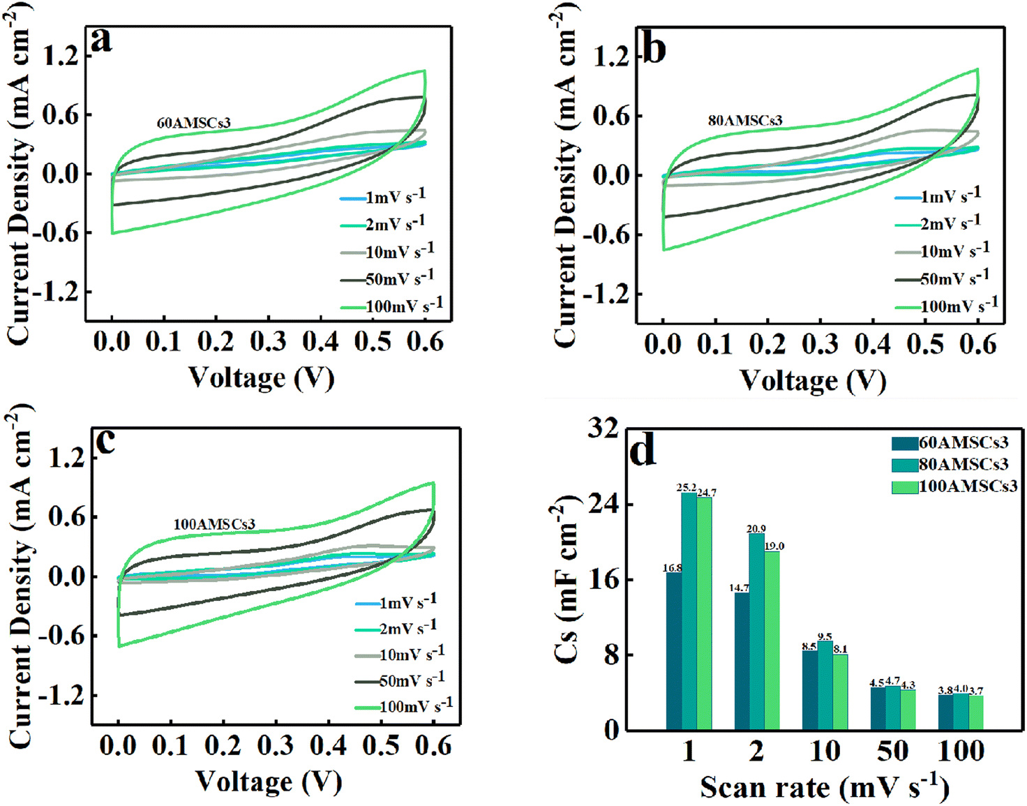 | ||
| Fig. 7 CVs for (a) 60AMSCs3, (b) 80AMSCs3, (c) 100AMSCs3 at 1–100 mV s−1 and (d) corresponding capacitance derived from CV profiles. | ||
To further investigate the capacitive behavior of these devices at ultra-fast charging/discharging rates, CV tests were conducted ranging from 10 to 50 V s−1. The examination results of 60AMSCs3, 80AMSCs3, and 100AMSCs3 are depicted in Fig. 8a–c, respectively. All these CV curves present a quasi-rectangle shape up to 50 V s−1, which is ≥50 times higher than that of rGO/V2O5 based PC-MSCs manufactured by combination of chemical synthesis, ultrasonication and spray deposition,74 rGO/VOx based PC-MSCs manufactured by combination of hydrothermal synthesis, ultrasonication, vacuum filtration and laser irradiation,49 and rGO-V2O5/graphene–vanadium nitride (VN) based PC-MSCs fabricated by combining hydrothermal synthesis, 3D printing and vacuum freeze-drying.83 This indicates the Mo@V–VO0.2 based PC-MSCs manufactured by WEDM technique achieved excellent capacitive properties at ultra-fast charging/discharging rate. It needs to note that this remarkable performance was obtained without any help from additional conductive media and other processing techniques. Fig. 8d showed that 80AMSCs3 achieved the larger capacitance value compared to the 60AMSCs3 and 100AMSCs3, and these results were consistent with those presented at Fig. 7. This phenomenon furtherly verified that the processing voltage has a great impact on the electrochemical properties of Mo@V–VO0.2 based PC-MSCs. The Mo@VO0.2 particles with relatively sparse distribution prepared by 60 V or with large agglomeration prepared by 100 V could not provide sufficient active sites for energy storage, which resulted in their relatively low capacity. The Mo@VO0.2 particles prepared by 80 V showed dense and uniform distribution, which facilitated more active sites for charge storage. Therefore, WEDM demonstrated its advantage in fabricating MSCs with customized performance by tailoring the surface morphology through its processing voltage.
 | ||
| Fig. 8 CVs for (a) 60AMSCs3, (b) 80AMSCs3, (c) 100AMSCs3 at 1–50 V s−1 and (d) corresponding capacitance derived from CV profiles. | ||
Fig. 6S† showed the GCD images of Mo@V–VO0.2 based 60AMSCs3, 80AMSCs3 and 100AMSCs3. Compared to those of 60AMSCs3 and 100AMSCs3, the Mo@V–VO0.2 based 80AMSCs3 obtained relatively longer discharge time indicating better capacitive performance, which agreed well with those obtained by CV curves (Fig. 7 and 8). As depicted in Fig. 9a, the Mo@V–VO0.2 based 80AMSCs3 showed small capacity decay and maintained a good capacity retention of 64.7% at 0.25–2 mA cm−2. In addition, the device demonstrated small capacity decay of 5.6% after 2000 cycles, which furtherly verified the good cycling stability of Mo@V–VO0.2 based 80AMSCs3 fabricated by one-step WEDM technique (Fig. 9b). This is due to the 3D binder-free V–VO0.2 integrated electrode design, surface morphology tailoring, Mo doping, introduction of oxygen vacancies and polyvalent state of VO0.2, which accelerates the electron/ion transportation efficiency and fully utilizes the advantage of the high capacitance of VO0.2 active material. Most importantly, the high-performance 3D Mo@V–VO0.2 based devices with customized electrochemical properties are prepared by a simple WEDM technology, without any help from additional conductive additives, templates, adhesives, expensive equipment, toxic solvents and other fabricated techniques. The developed WEDM manufacturing technique in this work provides a new way for scalable synthesis of metal oxide based materials and manufacturing of different energy storage devices with customized electrochemical performance.
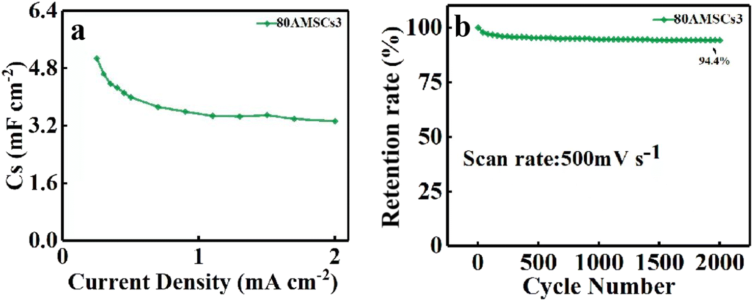 | ||
| Fig. 9 (a) Corresponding capacitance derived GCD profiles and (b) the capacitance retention of 80AMSCs3. | ||
4. Conclusion
In conclusion, a simple, safe, inexpensive, non-toxic, template-free, binder-free, environmentally-friendly and computer-aided design technique of WEDM has been developed for manufacturing arbitrary patterns of 3D Mo@V–VO0.2 based microdevices with customized electrochemical properties. The geometric structure of the microdevices was optimized via theoretical simulation and experiments. It was found that reduction of electrode width is beneficial for accelerating the ion transport rate. Moreover, the capacitive performance of Mo@V–VO0.2 based devices was optimized by WEDM processing voltage, which could directly tailor the surface morphology and particle distribution. Compared to 60AMSCs3 and 100AMSCs3 devices, 80AMSCs3 achieved a higher capacitance of 25.2 mF cm−2 (at 1 mV s−1). This is because the Mo@VO0.2 particles prepared by the processing voltage of 80 V are dense and uniform, providing more active sites for energy storage and thus enhance its electrochemical performance. Moreover, this 80AMSCs3 presents a quasi-rectangle CV shape up to 50 V s−1 and achieves a superior cyclic stability of 94.4% (2000), benefiting from the 3D binder-free V–VO0.2 integrated electrode design, surface morphology tailoring, Mo doping, introduction of oxygen vacancies and polyvalent state of VO0.2, which accelerates the electron/ion transportation efficiency and fully utilizes the advantage of the high capacitance of VO0.2 active material. This WEDM technique opens a new, simple, low-cost and high-precision strategy for synthesizing various metal oxides and constructing high-efficiency energy storage devices with customized performance for broad applications.Conflicts of interest
There are no conflicts to declare.Acknowledgements
Ri Chen appreciates for the funding projects of National Natural Science Foundation of China (Grant No. 52002085), Guangzhou Fundamental & Applied Research Foundation (Grant No. 2023A04J0278), Guangdong Provincial Department of Education (Grant No. 2022KTSCX069), Guangdong Provincial Special Fund for Science and Technology Innovation Policy (Grant No. pdjh2024a224), Youth Science and Technology Talent Lifting Project of Guangzhou Science and Technology Association (Grant No. QT2024-014) and Research & Development Start-up Fund of Guangdong Polytechnic Normal University (Grant No. 2021SDKYA106). Wenxia Wang thanks for the financial support from the funding projects of National Natural Science Foundation of China (Grant No. 22106020) and Guangdong Basic and Applied Basic Research Foundation (Grant No. 2024A1515030125). Lanying Xu appreciates for the funding projects of Guangdong Province Nature Science Foundation of China (Grant No. 2022A1515011065) and Guangdong Normal University of Technology (Grant No. 22GPNUZDJS21). Cheng Deng appreciates for National Natural Science Foundation of China (Grand No. 52374368), and the Guangdong Basic and Applied Basic Research Foundation (Grant No. 2023A1515012684).References
- S. Wang, J. Ma, X. Shi, Y. Zhu and Z. S. Wu, Recent status and future perspectives of ultracompact and customizable micro–supercapacitors, Nano Res. Energy, 2022, 1(2), e9120018 CrossRef.
- F. Bu, W. Zhou, Y. Xu, Y. Du, C. Guan and W. Huang, Recent developments of advanced micro–supercapacitors: design, fabrication and applications, npj Flexible Electron., 2020, 4(1), 1–16 CrossRef.
- R. Chen, Z. Xu, W. Xie, P. Deng, Y. Xu, L. Xu, G. Zhang, Y. Yang, G. Xie, I. Zhitomirsky and K. Shi, Fabrication of Fe–Fe1–xO based 3D coplanar microsupercapacitors by electric discharge rusting of pure iron substrates, RSC Adv., 2023, 13(38), 26995–27005 RSC.
- H. Zhang, Y. Cao, M. O. L. Chee, P. Dong, M. Ye and J. Shen, Recent advances in micro–supercapacitors, Nanoscale, 2019, 11(13), 5807–5821 RSC.
- J. F. Oudenhoven, L. Baggetto and P. H. Notten, All–solid–state lithium–ion microbatteries: a review of various three–dimensional concepts, Adv. Energy Mater., 2011, 1(1), 10–33 CrossRef CAS.
- X. Gan, J. Tang, X. Wang, L. Gong, I. Zhitomirsky, L. Qie and K. Shi, Aromatic additives with designed functions ameliorating chemo–mechanical reliability for zinc–ion batteries, Energy Storage Mater., 2023, 59, 102769 CrossRef.
- Y. Xu, P. Deng, R. Chen, W. Xie, Z. Xu, Y. Yang, D. Liu, F. Huang, Z. Zhuang and I. Zhitomirsky, Electric discharge direct writing of 3D Mo–MoOx pseudocapacitive micro–supercapacitors with designable patterns, Ceram. Int., 2023, 49(13), 22586–22594 CrossRef CAS.
- Y. Zhu, S. Wang, J. Ma, P. Das, S. Zheng and Z. S. Wu, Recent status and future perspectives of 2D MXene for micro–supercapacitors and micro–batteries, Energy Storage Mater., 2022, 51, 500–526 CrossRef.
- M. Beidaghi and Y. Gogotsi, Capacitive energy storage in micro–scale devices: recent advances in design and fabrication of micro–supercapacitors, Energy Environ. Sci., 2014, 7(3), 867–884 RSC.
- J. Zhang, G. Zhang, T. Zhou and S. Sun, Recent developments of planar micro–supercapacitors: fabrication, properties, and applications, Adv. Funct. Mater., 2020, 30(19), 1910000 CrossRef CAS.
- Y. Xu, S. Yu, H. M. Johnson, Y. Wu, X. Liu, B. Fang and Y. Zhang, Recent progress in electrode materials for micro–supercapacitors, Iscience, 2024, 27, 108786 CrossRef CAS PubMed.
- Z. Pan, S. Yu, L. Wang, C. Li, F. Meng, N. Wang, S. Zhou, Y. Xiong, Z. Wang and Y. Wu, Recent advances in porous carbon materials as electrodes for supercapacitors, Nanomaterials, 2023, 13(11), 1744 CrossRef CAS PubMed.
- P. Lamba, P. Singh, P. Singh, P. Singh, A. Kumar, M. Gupta and Y. Kumar, Recent advancements in supercapacitors based on different electrode materials: classifications, synthesis methods and comparative performance, J. Energy Storage, 2022, 48, 103871 CrossRef.
- Z. S. Wu, K. Parvez, X. Feng and K. Müllen, Photolithographic fabrication of high–performance all–solid–state graphene–based planar micro–supercapacitors with different interdigital fingers, J. Mater. Chem. A, 2014, 2(22), 8288–8293 RSC.
- W. Zhao, F. Liu, C. Liu, X. Li, L. Zhang and G. Zhang, Photolithographic fabrication of high–voltage output integrated all–solid–state planar on–chip micro-supercapacitors, Ferroelectrics, 2020, 563(1), 87–94 CrossRef CAS.
- S. Bellani, E. Petroni, A. E. Del Rio Castillo, N. Curreli, B. Martín-García, R. Oropesa-Nuñez, M. Prato and F. Bonaccorso, Scalable production of graphene inks via wet–jet milling exfoliation for screen–printed micro–supercapacitors, Adv. Funct. Mater., 2019, 29(14), 1807659 CrossRef.
- S. S. Delekta, A. D. Smith, J. Li and M. Östling, Inkjet printed highly transparent and flexible graphene micro–supercapacitors, Nanoscale, 2017, 9(21), 6998–7005 RSC.
- S. H. Park, G. Goodall and W. S. Kim, Perspective on 3D–designed micro–supercapacitors, Mater. Des., 2020, 193, 108797 CrossRef CAS.
- M. Z. Esfahani and M. Khosravi, Stamp–assisted flexible graphene–based micro–supercapacitors, J. Power Sources, 2020, 462, 228166 CrossRef CAS.
- J. Ye, H. Tan, S. Wu, K. Ni, F. Pan, J. Liu, Z. Tao, Y. Qu, H. Ji and P. Simon, Direct laser writing of graphene made from chemical vapor deposition for flexible, integratable micro–supercapacitors with ultrahigh power output, Adv. Mater., 2018, 30(27), 1801384 CrossRef PubMed.
- X. Shi, Z. Zeng, C. Liao, S. Tao, E. Guo, X. Long, X. Wang, D. Deng and Y. Dai, Flexible, planar integratable and all–solid–state micro–supercapacitors based on nanoporous gold/manganese oxide hybrid electrodes via template plasma etching method, J. Alloys Compd., 2018, 739, 979–986 CrossRef CAS.
- H. Xiao, Z. S. Wu, L. Chen, F. Zhou, S. Zheng, W. Ren, H. M. Cheng and X. Bao, One–step device fabrication of phosphorene and graphene interdigital micro–supercapacitors with high energy density, ACS Nano, 2017, 11(7), 7284–7292 CrossRef CAS PubMed.
- G. K. Veerasubramani, K. Krishnamoorthy and S. J. Kim, Electrochemical performance of an asymmetric supercapacitor based on graphene and cobalt molybdate electrodes, RSC Adv., 2015, 5(21), 16319–16327 RSC.
- S. Lochmann, J. Grothe, K. Eckhardt, D. Leistenschneider, L. Borchardt and S. Kaskel, Nanoimprint lithography of nanoporous carbon materials for micro–supercapacitor architectures, Nanoscale, 2018, 10(21), 10109–10115 RSC.
- H. Li, S. Liu, X. Li, Z. S. Wu and J. Liang, Screen–printing fabrication of high volumetric energy density micro–supercapacitors based on high–resolution thixotropic–ternary hybrid interdigital micro–electrodes, Mater. Chem. Front., 2019, 3(4), 626–635 RSC.
- C. Lethien, J. Le Bideau and T. Brousse, Challenges and prospects of 3D micro–supercapacitors for powering the internet of things, Energy Environ. Sci., 2019, 12(1), 96–115 RSC.
- X. Y. Fu, Z. D. Chen, D. D. Han, Y. L. Zhang, H. Xia and H. B. Sun, Laser fabrication of graphene–based supercapacitors, Photonics Res., 2020, 8(4), 577–588 CrossRef CAS.
- H. Liu, Z. Sun, Y. Chen, W. Zhang, X. Chen and C. P. Wong, Laser processing of flexible in–plane micro–supercapacitors: progresses in advanced manufacturing of nanostructured electrodes, ACS Nano, 2022, 16(7), 10088–10129 CrossRef CAS PubMed.
- R. Kumar, E. Joanni, R. Savu, M. S. Pereira, R. K. Singh, C. J. Constantino, L. T. Kubota, A. Matsuda and S. A. Moshkalev, Fabrication and electrochemical evaluation of micro–supercapacitors prepared by direct laser writing on free–standing graphite oxide paper, Energy, 2019, 179, 676–684 CrossRef CAS.
- H. Liu, K. S. Moon, J. Li, Y. Xie, J. Liu, Z. Sun, L. Lu, Y. Tang and C. P. Wong, Laser–oxidized Fe3O4 nanoparticles anchored on 3D macroporous graphene flexible electrodes for ultrahigh–energy in–plane hybrid micro–supercapacitors, Nano Energy, 2020, 77, 105058 CrossRef CAS.
- Y. Huang, H. Li, Z. Wang, M. Zhu, Z. Pei, Q. Xue, Y. Huang and C. Zhi, Nanostructured polypyrrole as a flexible electrode material of supercapacitor, Nano Energy, 2016, 22, 422–438 CrossRef CAS.
- R. Chen, M. Yu, R. P. Sahu, I. K. Puri and I. Zhitomirsky, The development of pseudocapacitor electrodes and devices with high active mass loading, Adv. Energy Mater., 2020, 10(20), 1903848 CrossRef CAS.
- R. Chen, I. Puri and I. Zhitomirsky, Polypyrrole–carbon nanotube–FeOOH composites for negative electrodes of asymmetric supercapacitors, J. Electrochem. Soc., 2019, 166(6), A935 CrossRef CAS.
- A. Eftekhari, L. Li and Y. Yang, Polyaniline supercapacitors, J. Power Sources, 2017, 347, 86–107 CrossRef CAS.
- B. Anothumakkool, R. Soni, S. N. Bhange and S. Kurungot, Novel scalable synthesis of highly conducting and robust PEDOT paper for a high performance flexible solid supercapacitor, Energy Environ. Sci., 2015, 8(4), 1339–1347 RSC.
- R. Chen, Y. Xiao and I. Zhitomirsky, FeOOH–polypyrrole–multiwalled carbon nanotube ternary nanocomposite fabricated by liquid–liquid co–extraction technique for supercapacitors application, Diamond Relat. Mater., 2023, 139, 110419 CrossRef CAS.
- D. Zhu, M. Yan, R. Chen, Q. Liu, J. Liu, J. Yu, H. Zhang, M. Zhang, P. Liu and J. Li, 3D Cu(OH)2 nanowires/carbon cloth for flexible supercapacitors with outstanding cycle stability, Chem. Eng. J., 2019, 371, 348–355 CrossRef CAS.
- M. Nawwar, R. Poon, R. Chen, R. P. Sahu, I. K. Puri and I. Zhitomirsky, High areal capacitance of Fe3O4–decorated carbon nanotubes for supercapacitor electrodes, Carbon Energy, 2019, 1(1), 124–133 CrossRef CAS.
- J. W. Lee, A. S. Hall, J. D. Kim and T. E. Mallouk, A facile and template–free hydrothermal synthesis of Mn3O4 nanorods on graphene sheets for supercapacitor electrodes with long cycle stability, Chem. Mater., 2012, 24(6), 1158–1164 CrossRef CAS.
- X. Gao, W. Wang, J. Bi, Y. Chen, X. Hao, X. Sun and J. Zhang, Morphology–controllable preparation of NiFe2O4 as high performance electrode material for supercapacitor, Electrochim. Acta, 2019, 296, 181–189 CrossRef CAS.
- O. Karatum, E. Yildiz, H. N. Kaleli, A. Sahin, B. Ulgut and S. Nizamoglu, RuO2 Supercapacitor Enables Flexible, Safe, and Efficient Optoelectronic Neural Interface, Adv. Funct. Mater., 2022, 32(31), 2109365 CrossRef CAS.
- S. Shinde, M. Jalak, G. Ghodake, N. Maile, V. Kumbhar, D. Lee, V. Fulari and D. Y. Kim, Chemically synthesized nanoflakes–like NiCo2S4 electrodes for high–performance supercapacitor application, Appl. Surf. Sci., 2019, 466, 822–829 CrossRef CAS.
- I. T. Bello, A. O. Oladipo, O. Adedokun and S. M. Dhlamini, Recent advances on the preparation and electrochemical analysis of MoS2–based materials for supercapacitor applications: A mini–review, Mater. Today Commun., 2020, 25, 101664 CrossRef CAS.
- Y. Zhou, L. Yin, S. Xiang, S. Yu, H. M. Johnson, S. Wang, J. Yin, J. Zhao, Y. Luo and P. K. Chu, Unleashing the Potential of MXene–Based Flexible Materials for High–Performance Energy Storage Devices, Advanced Science, 2024, 11(3), 2304874 CrossRef CAS PubMed.
- C. Liu, Y. Bai, W. Li, F. Yang, G. Zhang and H. Pang, In situ growth of three-dimensional MXene/metal–organic framework composites for high–performance supercapacitors, Angew. Chem., Int. Ed., 2022, 61(11), e202116282 CrossRef CAS PubMed.
- R. Liang, Y. Du, P. Xiao, J. Cheng, S. Yuan, Y. Chen, J. Yuan and J. Chen, Transition metal oxide electrode materials for supercapacitors: a review of recent developments, Nanomaterials, 2021, 11(5), 1248 CrossRef CAS PubMed.
- Y. Yan, B. Li, W. Guo, H. Pang and H. Xue, Vanadium based materials as electrode materials for high performance supercapacitors, J. Power Sources, 2016, 329, 148–169 CrossRef CAS.
- Z. Khan, P. Singh, S. A. Ansari, S. R. Manippady, A. Jaiswal and M. Saxena, VO2 Nanostructures for Batteries and Supercapacitors: A Review, Small, 2021, 17(4), e2006651 CrossRef PubMed.
- L. F. Zhang, J. Tang, S. Y. Liu, O. W. Peng, R. Shi, B. N. Chandrashekar, Y. Li, X. Li, X. N. Li, B. M. Xu and C. Cheng, A laser irradiation synthesis of strongly–coupled VOx–reduced graphene oxide composites as enhanced performance supercapacitor electrodes, Mater. Today Energy, 2017, 5, 222–229 CrossRef.
- B. A. Minyawi, M. Vaseem, N. A. Alhebshi, A. M. Al-Amri and A. Shamim, Printed Electrodes Based on Vanadium Dioxide and Gold Nanoparticles for Asymmetric Supercapacitors, Nanomaterials, 2023, 13(18), 1–14 CrossRef PubMed.
- H. Zhou, S. Zheng, X. Guo, Y. Gao, H. Li and H. Pang, Ordered porous and uniform electric–field–strength micro–supercapacitors by 3D printing based on liquid–crystal V2O5 nanowires compositing carbon nanomaterials, J. Colloid Interface Sci., 2022, 628, 24–32 CrossRef CAS PubMed.
- H. Zhou, G. Zhu, S. Dong, P. Liu, Y. Lu, Z. Zhou, S. Cao, Y. Zhang and H. Pang, Ethanol–Induced Ni2+–Intercalated Cobalt Organic Frameworks on Vanadium Pentoxide for Synergistically Enhancing the Performance of 3D–Printed Micro–Supercapacitors, Adv. Mater., 2023, 35(19), 2211523 CrossRef CAS PubMed.
- M. Dirican, M. Yanilmaz and X. Zhang, Free–standing polyaniline–porous carbon nanofiber electrodes for symmetric and asymmetric supercapacitors, RSC Adv., 2014, 4(103), 59427–59435 RSC.
- Y. Qu, Y. Zhou, Q. Yang, J. Cao, Y. Liu, X. Qi and S. Jiang, Lignin–Derived Lightweight Carbon Aerogels for Tunable Epsilon–Negative Response, Advanced Science, 2024, 2401767 CrossRef CAS PubMed.
- Y. P. Qu, Y. L. Zhou, Y. Luo, Y. Liu, J. F. Ding, Y. L. Chen, X. Gong, J. L. Yang, Q. Peng and X. S. Qi, Universal paradigm of ternary metacomposites with tunable epsilon–negative and epsilon–near–zero response for perfect electromagnetic shielding, Rare Met., 2024, 43(2), 796–809 CrossRef CAS.
- A. Abdisattar, M. Yeleuov, C. Daulbayev, K. Askaruly, A. Tolynbekov, A. Taurbekov and N. Prikhodko, Recent advances and challenges of current collectors for supercapacitors, Electrochem. Commun., 2022, 142, 107373 CrossRef CAS.
- A. Abdisattar, M. Yeleuov, C. Daulbayev, K. Askaruly, A. Tolynbekov, A. Taurbekov and N. Prikhodko, Recent advances and challenges of current collectors for supercapacitors, Electrochem. Commun., 2022, 107373 CrossRef CAS.
- Y. Xie, J. Zhang, H. Xu and T. Zhou, Laser–assisted mask–free patterning strategy for high-performance hybrid micro–supercapacitors with 3D current collectors, Chem. Eng. J., 2022, 437, 135493 CrossRef CAS.
- Q. Jiang, N. Kurra, C. Xia and H. N. Alshareef, Hybrid Microsupercapacitors with Vertically Scaled 3D Current Collectors Fabricated using a Simple Cut–and–Transfer Strategy, Adv. Energy Mater., 2017, 7(1), 1–9 CAS.
- A. Kumar, D. V. Kumar and D. J. Kumar, A review on the state of the art in wire electric discharge machining (WEDM) process, Int. J. Mech. Prod. Eng. Res. Dev., 2011, 1(1), 23–39 Search PubMed.
- S. Vijayabhaskar, T. Rajmohan, T. P. Sisir, J. P. Abishek and R. M. Reddy, Review of WEDM studies on metal matrix composites, IOP Conf. Ser.: Mater. Sci. Eng., 2018, 012051 Search PubMed.
- Y. Xu, P. Deng, R. Chen, W. Xie, Z. Xu, Y. Yang, D. Liu, F. Huang, Z. Zhuang and I. Zhitomirsky, Electric discharge direct writing of 3D Mo–MoOx pseudocapacitive micro–supercapacitors with designable patterns, Ceram. Int., 2023, 49(13), 22586–22594 CrossRef CAS.
- R. Chen, Z. Xu, W. Xie, P. Deng, Y. Xu, L. Xu, G. Zhang, Y. Yang, G. Xie and I. Zhitomirsky, Fabrication of Fe–Fe1− xO based 3D coplanar microsupercapacitors by electric discharge rusting of pure iron substrates, RSC Adv., 2023, 13(38), 26995–27005 RSC.
- A. Roy and S. Narendranath, Effect of spark gap voltage and wire electrode feed rate on machined surface morphology during Wire EDM process, Mater. Today: Proc., 2018, 5(9), 18104–18109 Search PubMed.
- F. Wang, B. Xu, H. Wan, J. Yang, B. Yang and W. Jiang, Preparation of vanadium powders by calcium vapor reduction of V2O3 under vacuum, Vacuum, 2020, 173, 109133 CrossRef CAS.
- G. Silversmit, D. Depla, H. Poelman, G. B. Marin and R. De Gryse, Determination of the V2p XPS binding energies for different vanadium oxidation states (V5+ to V0+), J. Electron Spectrosc. Relat. Phenom., 2004, 135(2–3), 167–175 CrossRef CAS.
- X. Pan, G. Ren, M. N. F. Hoque, S. Bayne, K. Zhu and Z. Fan, Fast supercapacitors based on graphene–bridged V2O3/VOx core–shell nanostructure electrodes with a power density of 1 MW kg−1, Adv. Mater. Interfaces, 2014, 1(9), 1400398 CrossRef.
- J. J. Ye, P. H. Li, H. R. Zhang, Z. Y. Song, T. Fan, W. Zhang, J. Tian, T. Huang, Y. Qian and Z. Hou, Manipulating Oxygen Vacancies to Spur Ion Kinetics in V2O5 Structures for Superior Aqueous Zinc–Ion Batteries, Adv. Funct. Mater., 2023, 33(46), 2305659 CrossRef CAS.
- X. Liang, L. Yan, W. Li, Y. Bai, C. Zhu, Y. Qiang, B. Xiong, B. Xiang and X. Zou, Flexible high–energy and stable rechargeable vanadium–zinc battery based on oxygen defect modulated V2O5 cathode, Nano Energy, 2021, 87, 106164 CrossRef CAS.
- J. Song, X. Gu, Y. Cao and H. Zhang, Porous oxygen vacancy–rich V2O5 nanosheets as superior semiconducting supports of nonprecious metal nanoparticles for efficient on–demand H2 evolution from ammonia borane under visible light irradiation, J. Mater. Chem., 2019, A7(17), 10543–10551 RSC.
- Z. Jiang, H. Yang, L. Cao, Z. Yang, Y. Yuan and E. Li, Enhanced breakdown strength and energy storage density of lead–free Bi0.5Na0.5TiO3–based ceramic by reducing the oxygen vacancy concentration, Chem. Eng. J., 2021, 414, 128921 CrossRef CAS.
- D. Gao, J. Zhang, G. Yang, J. Qi, M. Si and D. Xue, Ferromagnetism induced by oxygen vacancies in zinc peroxide nanoparticles, J. Phys. Chem. C, 2011, 115(33), 16405–16410 CrossRef CAS.
- A. Dewan, R. Narayanan and M. O. Thotiyl, A multi–chromic supercapacitor of high coloration efficiency integrating a MOF–derived V2 O5 electrode, Nanoscale, 2022, 14(46), 17372–17384 RSC.
- B. D. Boruah, S. Nandi and A. Misra, Layered assembly of reduced graphene oxide and vanadium oxide heterostructure supercapacitor electrodes with larger surface area for efficient energy–storage performance, ACS Appl. Energy Mater., 2018, 1(4), 1567–1574 CrossRef CAS.
- Z. Liu, Z. S. Wu, S. Yang, R. Dong, X. Feng and K. Müllen, Ultraflexible in–plane micro–supercapacitors by direct printing of solution–processable electrochemically exfoliated graphene, Adv. Mater., 2016, 28(11), 2217–2222 CrossRef CAS PubMed.
- Q. Jiang, C. Wu, Z. Wang, A. C. Wang, J. H. He, Z. L. Wang and H. N. Alshareef, MXene electrochemical microsupercapacitor integrated with triboelectric nanogenerator as a wearable self–charging power unit, Nano Energy, 2018, 45, 266–272 CrossRef CAS.
- Y. Yang, L. He, C. Tang, P. Hu, X. Hong, M. Yan, Y. Dong, X. Tian, Q. Wei and L. Mai, Improved conductivity and capacitance of interdigital carbon microelectrodes through integration with carbon nanotubes for micro–supercapacitors, Nano Res., 2016, 9, 2510–2519 CrossRef CAS.
- D. Pech, M. Brunet, P. L. Taberna, P. Simon, N. Fabre, F. Mesnilgrente, V. Conédéra and H. Durou, Elaboration of a microstructured inkjet–printed carbon electrochemical capacitor, J. Power Sources, 2010, 195(4), 1266–1269 CrossRef CAS.
- D. Pech, M. Brunet, H. Durou, P. Huang, V. Mochalin, Y. Gogotsi, P. L. Taberna and P. Simon, Ultrahigh–power micrometre–sized supercapacitors based on onion–like carbon, Nat. Nanotechnol., 2010, 5(9), 651–654 CrossRef CAS PubMed.
- Z. S. Wu, K. Parvez, X. Feng and K. Müllen, Graphene–based in–plane micro-supercapacitors with high power and energy densities, Nat. Commun., 2013, 4(1), 2487 CrossRef PubMed.
- M. F. El-Kady and R. B. Kaner, Scalable fabrication of high–power graphene micro-supercapacitors for flexible and on–chip energy storage, Nat. Commun., 2013, 4(1), 1475 CrossRef PubMed.
- W. Gao, N. Singh, L. Song, Z. Liu, A. L. M. Reddy, L. Ci, R. Vajtai, Q. Zhang, B. Wei and P. M. Ajayan, Direct laser writing of micro–supercapacitors on hydrated graphite oxide films, Nat. Nanotechnol., 2011, 6(8), 496–500 CrossRef CAS PubMed.
- K. Shen, J. Ding and S. Yang, 3D printing quasi–solid–state asymmetric micro–supercapacitors with ultrahigh areal energy density, Adv. Energy Mater., 2018, 8(20), 1800408 CrossRef.
Footnote |
| † Electronic supplementary information (ESI) available. See DOI: https://doi.org/10.1039/d4ra04909h |
| This journal is © The Royal Society of Chemistry 2024 |