
 Open Access Article
 This Open Access Article is licensed under a Creative Commons Attribution-Non Commercial 3.0 Unported Licence
Experimental observation and characterization of amorphous carbon generated in graphene on gold nanoparticles†
Surjyasish Mitra a,
Natalie Hamadab and
Sushanta K. Mitra*a
a,
Natalie Hamadab and
Sushanta K. Mitra*a
aDepartment of Mechanical & Mechatronics Engineering, Waterloo Institute for Nanotechnology, University of Waterloo, Waterloo, Ontario N2L 3G1, Canada. E-mail: skmitra@uwaterloo.ca
bCanadian Centre for Electron Microscopy, McMaster University, 1280 Main St W, Hamilton, ON L8S 4L8, Canada. E-mail: hamadan@mcmaster.ca
First published on 12th August 2024
Abstract
The interaction of graphene with gold nanoparticles is investigated using transmission electron microscopy. We observe gold-nanoparticle-mediated etching of graphene flakes, often leading to hole formation. Further, using a combination of high-angle annular dark field imaging and electron energy loss spectroscopy, we highlight that the catalytic effects of gold nanoparticles on graphene lead to the formation of amorphous carbon layers. From the extracted diffractograms, we observe regions with diffraction halos as well as some regions with a weak tetrahedral motif. Using independently performed Raman measurements, we confirm the presence of tetrahedral amorphous carbon as well as mixed graphitic–amorphous regions. For the amorphous carbon regions with mixed sp2–sp3 states, the Raman G peak is red-shifted to 1564 cm−1 and an ID/IG ratio of 0.63 indicates less than 20% sp3 content. For the tetrahedral amorphous carbon regions, we observe that the Raman G peak is at 1580 cm−1, close to that of monolayer graphene. However, there is no Raman D peak, i.e., ID/IG = 0, which indicates close to 100% sp3 content. The translation of the Raman G peak location and the ID/IG ratios is on par with the amorphization trajectory analysis of Ferrari and Robertson (Phys. Rev. B: Condens. Matter Mater. Phys., 2000, 61, 14095) and validates the conversion route of graphite to amorphous carbon to tetrahedral amorphous carbon. The presented method provides a promising pathway for creating defect-induced amorphous carbon at room temperature, which has a broader impact on the electronics and semiconductor industries.
1 Introduction
Defects in graphene can either be natural defects, such as topological defects, vacancies, or carbon ad-atoms, or externally induced ones, such as foreign ad-atoms and impurities.1–3 As technology moves towards integrating graphene-based devices,4–6 understanding the interaction of graphene with foreign atoms becomes increasingly relevant. In this regard, metal ad-atoms or nanoparticles are primarily investigated, since in most devices metal deposition or metal electrodes are an integral part.7,8 Consequently, the interaction of graphene with metals as controlled dopants or defects has been extensively investigated and a plethora of interesting observations have been made.2,7,9–11 Ad-atoms of transition metals, like gold (Au), chromium (Cr), nickel (Ni), etc., are expected to bond covalently with graphene, causing lattice distortions.10 In effect, they can significantly reduce the defect formation energy, leading to defect propagation in the graphene sheets. This has been experimentally demonstrated by Ramasse et al., where they observed significant etching of freely suspended graphene at the edges mediated by the controlled presence of metal ad-atoms, like Cr, Ni, and Al.9 At the same time, partial oxidation has been proposed to be also responsible for the etching process, often leading to hole formation on the top of the graphene sheets.9Transition-metal-mediated catalytic oxidation or hydrogenation of graphite had been observed some thirty years before the discovery of graphene, where the formation of nanoscale channels was observed due to the etching of graphite.12 In recent times, Ni-nanoparticle-assisted catalytic hydrogenation and subsequent etching have been proposed to be an effective method to cut graphene with nanoscale precision.13 Further, metals like Au have been extensively probed as a growth substrate for graphene. Nie et al. observed the formation of dendritic graphene patterns for graphene grown on an Au(111) substrate at high temperatures.14 Biroju et al. observed enhanced interaction between Au and defective graphene layers for Au films/nanoparticles deposited on graphene grown using chemical vapor deposition.15 Turchanin et al. observed patches of amorphous carbon formation during graphene growth using aromatic self-assembled monolayers on an Au substrate. They observed ordered (graphene nanosheets) and less-ordered (amorphous carbon) regions bonded in a 2D network.16 This raises the possibility that incorporating metals like Au as controlled defects in the graphitic system can induce amorphous carbon formation by limiting the formation of sp2 bonds – an area seldom explored.
The crystalline analogue of amorphous carbon, i.e., graphene/graphite, has a well-known hexagonal network of sp2 hybridized carbon atoms with a centered bond length of 1.42 Å and interlayer spacing of 3.4 Å.17,18 Amorphous carbon (a-C), on the other hand, lacks long-range periodicity and can have a mixture of sp, sp2 and sp3 orbital states.19,20 Consequently, a-C can exhibit mixed states with varying sp3 (or sp2) fractions. Depending on the relative fraction of sp3 and sp2 states, a-C can be diamond-like, tetrahedral, etc.20 Further, it can exhibit a broad range of bond lengths, bond angles, stiffness, density, and electronic properties. Recent experiments on monolayer amorphous carbon have exhibited sp3/sp2 ratios of 0.2–0.4 as well as bond lengths varying between 0.9–1.8 Å.21 However, for those experiments, conventional techniques like physical vapor deposition (PVD)22 and chemical vapor deposition (CVD)23 were employed. Joo et al. demonstrated the growth of a one-atom-thick amorphous carbon layer on germanium substrates using a mixture of methane and hydrogen gases at a temperature of 900 °C.24 Other carbonaceous gases like C2H2 in combination with H2 have also been used for the synthesis of large-area a-C.25 Further, Toh et al. synthesized monolayer a-C using laser-assisted CVD at temperatures ranging from 200–600 °C.21 The common theme for CVD-based deposition techniques is the use of high temperatures. PVD techniques like sputtering26 and vacuum arc deposition27 have also been successfully employed to generate a-C films. Here also, the use of high temperature/pressure/current is an integral part.
In contrast, defect-induced mixed sp2–sp3 states and amorphous carbon formation have been investigated relatively less,28 and thus are not completely understood. This is true for amorphous materials in general, where their fundamental properties are still not well understood due to insufficient knowledge of their atomic structures, which appears to be a direct consequence of limited experimental characterization. At the same time, amorphous materials are increasingly used in a wide range of applications in the semiconductor industry.19,29–31 Among these, amorphous silicon thin films, amorphous metal oxide semiconductors, and amorphous carbon films are much desired for use in LCD/LED displays,32 hard masks for advanced manufacturing,33,34 battery technology,35,36 and energy devices.37,38 Thus, at a time when amorphous carbon materials are becoming increasingly relevant, a comprehensive understanding of their atomic structures and properties, and seeking alternative routes for their generation, become necessary.
In this work, we report a scanning transmission electron microscopy (STEM) study of graphene on gold nanoparticles (AuNPs). 35 nm AuNPs are deposited on lacey carbon TEM grids and graphene/graphite flakes are subsequently transferred onto them (see Materials and methods). Consequently, using a combination of bright-field (BF) TEM, high-angle annular dark-field (HAADF) STEM, and electron energy loss spectroscopy (EELS) (see Materials and methods), we reveal how the catalytic effects of AuNPs create various defects in graphene and lead to the generation of mixed graphitic–amorphous carbon states. Further, electron diffraction signatures and Raman spectroscopy measurements (see Materials and methods) provide us with valuable insights into the amorphous carbon states thus observed.
2 Materials and methods
2.1 Sample preparation
Gold nanoparticle (AuNP) seeds with a mean diameter of 15 nm were synthesized using the classical Frens method. First, 100 mL 0.01 wt% HAuCl4 aqueous solution was heated to boiling conditions under continuous stirring. Upon boiling, 2 mL 1 wt% of Na3C6H5O7 aqueous solution was added immediately. After around 10 minutes, the color of the solution gradually changed from light yellow to dark and finally turned to wine red, which indicated the formation of AuNPs. The mixed solution was kept heated and stirred for another 20 minutes and cooled down to room temperature. The obtained AuNPs with an average diameter of 13 nm served as Au seeds. The solution was stored in the refrigerator at 4 °C before further use. 25 nm AuNPs were prepared via the seed growth method using 13 nm Au as seeds. Briefly, 25 mL Au NP seed (13 nm) solution, 1 mL 1 wt% polyvinylpyrrolidone (PVP) solution, 1 mL 1 wt% Na3C6H5O7 and 25 mL NH2OH–HCl (25 mM) solution were combined at room temperature (25 °C). After mixing thoroughly, 25 mL of HAuCl4 (0.1 wt%) solution was added to the above solution drop by drop within 25 min under constant stirring. Then, the mixed solution was kept under stirring conditions for another 20 min to ensure the reaction was complete. The final color of the solution was dark wine-red, indicating the formation of 35 nm AuNPs. The final solution was transferred to lacey carbon-based Cu TEM grids (Ted Pella) via drop casting and a wait time was maintained for drying.Natural graphite crystals (NGS Trading Gmbh) were used to obtain the graphene flakes on Si/SiO2 substrates via mechanical exfoliation using Scotch tape (3M). The substrates were observed under an optical microscope and regions with mono- and few-layer graphene were identified using color contrast. Subsequently, a scratch was made using a Stanley knife and the flakes were picked up. The flakes were dispersed in isopropyl alcohol (IPA) and sonicated for 15 min. The flakes were then transferred onto the TEM grids with AuNPs using drop casting and a wait time was maintained for the solvent to evaporate.
2.2 TEM measurements
Initial transmission electron microscopy measurements (Fig. 1) were performed in a Zeiss Libra 200 MC TEM at 60 kV. All other TEM measurements were performed in a Fisher Spectra Ultra TEM at 60 kV and a vacuum of 3 × 10⁻⁸ torr. The typical probe size for the STEM imaging was 0.5 nm. The high-angle annular dark-field (HAADF) detector has convergence and collection semi-angles of 28 mrad and 60 mrad, respectively. High-resolution TEM (HRTEM) images were acquired using a Ceta CMOS detector (Thermo Fisher Scientific). EELS data were collected using a GIF Continuum S (Gatan). The beam current for EELS chemical analysis was 0.25 nA and the probe size was 0.5 nm. All EELS data were processed using Gatan Digital Micrograph software, version 3.5. The internal standard function in GMS (Hartree Slater model) was used to evaluate carbon K-edge energy-loss near-edge structure (ELNES) regions and produce corresponding maps.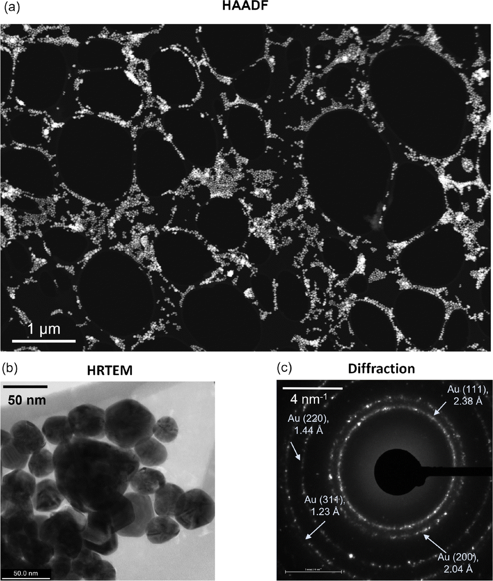 | ||
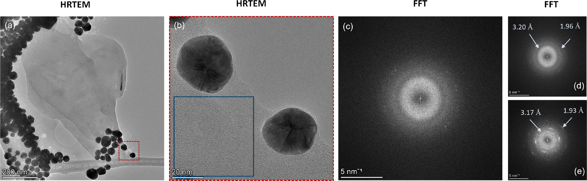
| Fig. 1 (a) High-angle annular dark-field (HAADF) STEM image of a lacey carbon-based TEM grid with gold nanoparticle (AuNP) deposition. (b) Representative high-resolution TEM (HRTEM) image of a cluster of AuNPs. (c) Electron diffraction pattern of the AuNPs highlighting the different Miller indices. The indicated d-spacing is calculated from the radius of the observed rings in reciprocal space. | ||
2.3 Raman measurements
A Renishaw inVia Reflex Raman spectroscopy system equipped with a 532 nm laser (Renishaw DPSSL laser, 50 mW) was employed for Raman measurements. The laser filtered to 1% intensity was focused on the samples using a 50× objective lens with a laser spot size of 4 μm. The Raman scattered light was analyzed using a 2400 lines per mm grating. This provided a Raman shift spacing of 1.2 cm−1 between individual data points. The Raman spectra were acquired between 1000 and 3000 cm−1 with a typical acquisition time of 10–20 s. For fitting the experimentally obtained Raman spectrum, we used the Lorentz function. Unlike the TEM measurements, the samples, i.e., AuNPs and graphene, were prepared on Si/SiO2 substrates for Raman measurements. First, the AuNPs were deposited on the substrates and consequently the graphene was deposited using mechanical exfoliation from natural graphite crystals.3 Results and discussions
Fig. 1a shows a relatively low-magnification HAADF image of the AuNP distribution on the TEM grid. The distribution is uniform at most locations across the TEM grid, while cluster formation occurs in some regions. High-resolution TEM (HRTEM) imaging and subsequent particle size analysis confirm that the mean and median diameters of the Au nanoparticles are 36 nm and 34 nm, respectively (excluding large clusters) (Fig. 1b), while the standard deviation is 11 nm (Fig. S1, ESI†). Note that this distribution of AuNPs may vary with the underlying substrate, for example, silicon. Further, the electron diffraction signature confirms the FCC structure of gold with Miller indices (111), (200), (220), and (331) (Fig. 1c).39 Subsequently, we experimentally analyzed how the AuNPs interact with graphene upon its deposition. For one to a few layers of graphene deposition, we observe that a certain fraction of AuNPs prefer to reside on top of the freely suspended graphene/graphite flakes. Here, we note that most AuNPs occupy places on top of the TEM grid. Compared to that, a relatively small fraction of nanoparticles are on top of the flakes, while some are at the edges where the lacey carbon-based TEM grid meets the suspended graphene flakes (Fig. 2).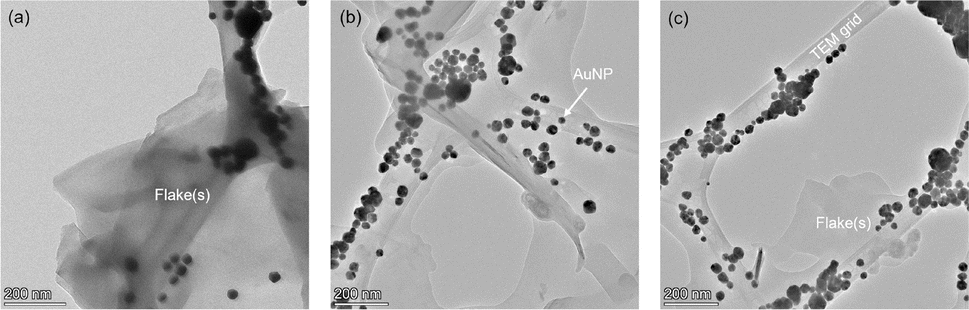 | ||
| Fig. 2 (a)–(c) High-resolution TEM (HRTEM) snapshots of different regions of the TEM grid highlighting the presence of graphene/graphite flakes and gold nanoparticles (AuNPs). The distribution of the AuNPs is predominantly along the TEM grid while some nanoparticles are observed to sit on top of the graphene flakes. | ||
Among the few overlapping graphene flakes observed using HRTEM, we isolate one monolayer to observe any morphological change due to the neighboring presence of AuNPs (Fig. 3a). We confirm the flake to be a monolayer using the corresponding Fast Fourier Transform (FFT) signature where the hexagonal motif is visible (Fig. 3b). On closer inspection of the monolayer with neighboring AuNPs, we observe that certain regions of the monolayer flake have been etched away, leaving the lattice network broken (Fig. 3c). The width of the etched regions or holes varies from a few nanometers to around 70 nm (Fig. 3c). An enlarged view of a particular etched hole is shown in Fig. 3d. We also observe that the edges of the monolayer flake, as well as the neighbouring flakes, are very sharp, possibly due to etching. We note that the etching of graphene in the presence of metal ad-atoms like Ni, Cr, etc., has been previously reported by Ramasse et al.,9 but no such observations were found for Au. Thus, we hypothesize that the residual adsorbed oxygen in the samples along with catalytic AuNPs may have likely triggered the etching phenomena, leading to hole formation. However, we observe that the hole regions are relatively far away from the location of the AuNPs and thus the onset of etching is not at the AuNP site. Furthermore, we note that the presence of AuNPs is expected to cause charge transfer to graphene, making the graphene slightly p-doped.7 Such a charge transfer mechanism may also make some contribution towards the etching phenomenon. In contrast, no such etching-induced hole formation was observed for graphene-only samples without AuNP deposition (Fig. S2, ESI†).
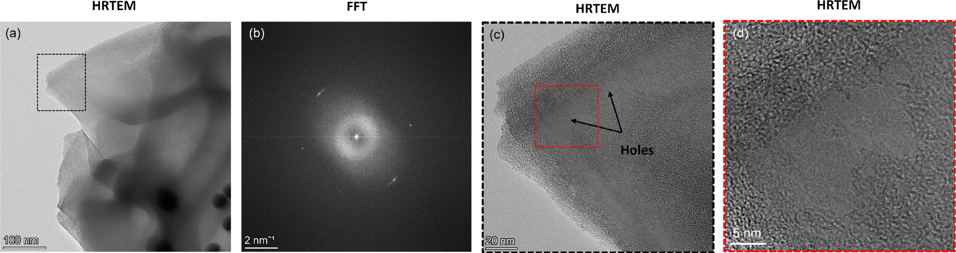 | ||
| Fig. 3 (a) High-resolution TEM (HRTEM) image of a collection of graphene flakes with gold nanoparticles (AuNPs) in the vicinity (dark circles in bottom right corner). (b) Fast Fourier Transform (FFT) signature of the outermost protruding monolayer graphene in (a), highlighted by black dotted box. The hexagonal motif with six carbon atoms can be seen. (c) Close-up of the black dotted box region shown in (a). The graphene flake exhibits the formation of holes. (d) An enlarged view of the hole formation for the red dotted box region shown in (c). | ||
To further explore this catalytic effect of AuNPs on graphene, we perform detailed Z-contrast HAADF imaging in combination with EELS chemical analysis. In recent times, mapping chemical signatures using EELS has proved to be an efficient method to identify chemical compositions40 and bonding states,41,42 and even visualize single atoms in extreme confinement.43 On the one hand, the Z-contrast mode of HAADF enables imaging across different Z-directions of a particular field of view. On the other hand, using EELS elemental analysis, we can select a cross-section of any particular Z-slice and identify the elements present there from the intensity information (no. of counts). Consequently, we can determine all the elements present in the scanned image and highlight the elements using an elemental map.43 For instance, for identifying the presence of carbon atoms in graphene/graphite, the EELS elemental map of the carbon K-edge (284 eV) provides us with the required confirmation.
In Fig. 4a, we show the HAADF-EELS visualization of a collection of overlapping graphene flakes in the presence of gold nanoparticles. Interestingly, upon EELS elemental analysis, we observe the presence of amorphous carbon. While the energy loss count spectrum of graphitic carbon (Fig. 4c) exhibits two sharp peaks corresponding to σ* and π* contributions,42,43 and a third peak, the spectrum for amorphous carbon (Fig. 4b) exhibits a broad π* peak44,45 and no third peak. In Fig. 4d, the Au EELS spectrum corresponding to the AuNPs is shown for clarity. Trace amounts of nitrogen and oxygen are also observed from our EELS elemental analysis (Fig. S3, ESI†). Interestingly, we observe that most of the oxygen appears on the AuNP sites, whereas nitrogen appears mostly around the carbon edges (Fig. S3, ESI†). From the above observation, it is evident that significant destruction of graphene is indeed occurring in the presence of AuNPs. The probable cause is the presence of oxygen or hydroxyl end groups on the AuNPs, as evident from the EELS signature of oxygen and Au, possibly activating a catalytic process. Further, the catalytic destruction of sp2-hybridized carbon atoms in graphene leads to the formation of amorphous carbon patches with significant coverage across the flakes. The amorphous carbon formation in other areas of the TEM grid is further shown in Fig. S4, ESI†.
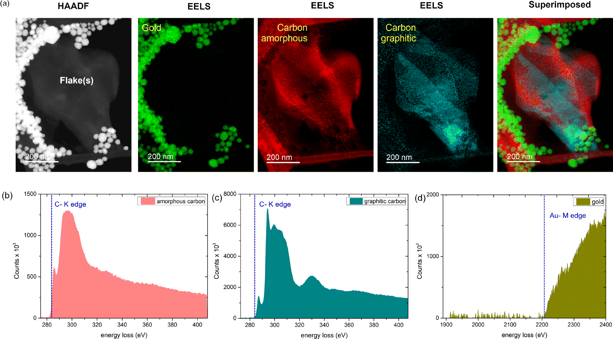 | ||
| Fig. 4 (a) HAADF image of a collection of graphene flakes with gold nanoparticles (AuNPs), and corresponding EELS elemental mapping signatures of AuNPs, amorphous carbon, and graphitic carbon. The final image is the superimposed elemental map of all the elements. The color assignment is arbitrary. (b)–(d) Representative EELS spectra for amorphous carbon, graphitic carbon, and gold, respectively, obtained at their respective locations in the image. The C-K edge at 284 eV and Au-M edge at 2206 eV are highlighted. | ||
Here, we further analyze the observed formation of amorphous carbon. To do so, we select an area from the corresponding HRTEM image (Fig. 5a and b) of the HAADF image shown in Fig. 4 with amorphous carbon presence and highlight its FFT signature. We observe a diffraction halo with two rings (Fig. 5c), similar to that observed in recent work where monolayer amorphous carbon was synthesized using laser-assisted CVD.21 However, in contrast to that work, where it was solely an amorphous carbon monolayer, here the observed region can also be a mixed graphitic–amorphous state. Further, the FFT signature in another location of the grid (see Fig. S5, ESI†) also exhibited halos, however with a weak tetrahedral motif, i.e., four carbon atoms (Fig. 5e). A weak tetrahedral motif possibly indicates the formation of purely tetrahedral amorphous carbon with very little graphitic presence. Upon analysis of both the diffraction patterns, we observe that the radii of the two rings in both the patterns are similar. In other words, the d-spacing calculated in the reciprocal space from the measured radii of the rings is consistent (Fig. 5d and e). The d-spacing calculated from the diffraction pattern essentially provides the interlayer distance between neighbouring planes of carbon atoms. For a few layers of graphene (or graphite), it is 3.4 Å. Here, we observe that for amorphous carbon, the interlayer spacing is around 3.17–3.20 Å (Fig. 5d and e), i.e., approximately 6% less than that of graphene. To verify that we have regions with amorphous carbon and mixed amorphous–graphitic states, we perform Raman measurements. Here, we note that even though the minimum resolution of TEM, dictated by the electron probe size of 0.5 nm, is orders of magnitude smaller than the resolution of Raman spectroscopy, dictated by the laser spot size of 4 μm, since the region of interest in our TEM measurements is around 1.2 μm × 0.9 μm (Fig. 4a), our Raman measurements are not obscured by this scale disparity and can provide a reasonable characterization of the graphene–AuNP system.
 | ||
| Fig. 5 (a) High-resolution TEM (HRTEM) image of the graphene on AuNPs corresponding to the HAADF image shown in Fig. 4. (b) An enlarged view of the cross-section (red box) shown in (a). (c) The FFT signature of the cross-section shown as a blue box in (b). The pattern exhibits a halo. (d) Analysis of the FFT signature shown in (c). The d-spacing is calculated using the radius of the rings in reciprocal space. (e) FFT signature of another region with mixed graphitic–amorphous presence. The diffraction signature is a halo with a weak tetrahedral motif showing four carbon atoms. The d-spacing is calculated using the radius of the rings in reciprocal space. | ||
In Fig. 6, we show the Raman signature for the graphene on the AuNP system. Here, we note that for Raman measurements, the AuNPs were grown on Si/SiO2 substrates and subsequently graphene was transferred. Note that since neither graphene nor AuNPs are reactive with either the Cu TEM grids or the Si/SiO2 substrates, the change of underlying substrate for the Raman measurements does not affect our generic findings. Raman signatures of single or multi-layer graphene on different substrates are well reported46,47 and we do not elaborate on that here. Rather, we focus primarily on the Raman signature of regions with amorphous carbon presence. Also, existing literature has extensively probed the enhancement of the Raman signature of graphene due to an underlying Au substrate, i.e., the surface-enhanced-Raman-spectroscopy (SERS) effect,15,48,49 and we do not elaborate on that further in the present work. After a thorough scan of the graphene flakes on the Si/SiO2 substrate with AuNPs, we primarily obtain three different spectra: one corresponding to the graphitic portion of the flake (without defects, Fig. 6a) and the other two in regions with the supposed presence of disordered states: either amorphous carbon or mixed states (Fig. 6b and c). As shown in Fig. 6a, the first Raman spectrum corresponding to the graphitic portion exhibits the commonly observed G and 2D peaks at 1581 cm−1 and 2723 cm−1, respectively. For the regions with disordered, amorphous states, the Raman G peak is present in both cases, but one of the spectra has a D peak (Fig. 6b) while the other one does not (Fig. 6c). The Raman D peak occurs due to the presence of defects and also indicates the presence of both sp2 and sp3 carbons. Further, a complete absence of the Raman D peak occurs either for pristine graphene/graphite (purely sp2-hybridized carbon) or pristine diamond-like carbon (purely sp3-hybridized carbon). Here, we note that it is well established that amorphous or even mixed states do not have a 2D Raman peak50 and is a confirmation of sorts of the amorphous carbon presence.
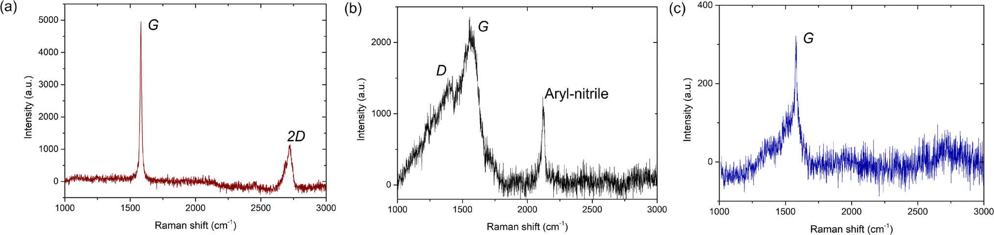 | ||
| Fig. 6 (a) Raman spectrum of the graphitic portion of the flake. (b) and (c) Raman spectra of the non-graphitic, disordered, amorphous carbon. The Raman G, D, and 2D peaks are highlighted. The graphene is transferred onto Si/SiO2 substrates with gold nanoparticles. | ||
For the second Raman spectrum, we observe that the Raman G peak is around 1564 cm−1, whereas the location of the Raman D peak is around 1369 cm−1 (Fig. 6b). Compared to the graphitic portion of the flake (Fig. 6a) or even monolayer/multilayer graphene on Si/SiO2 substrates without AuNP deposition, whose G peak is at 1581 cm−1 (ref. 46 and 47) (see Fig. S6 and S7, ESI†), here the G peak is red-shifted by 17 cm−1. Also, in comparison to graphene, where the D peak is ideally at 1350 cm−1,46,47 here the D peak is blue-shifted by 19 cm−1. Further, the full-width at half maximum (FWHM) of the Raman G peak is 117 ± 3 cm−1 (see Fig. S6, ESI†) and thus considerably broad, as commonly observed for amorphous carbon.20,50–52 Here, we note that for mixed sp2–sp3 states, the relative intensity of the D and G peaks, i.e., ID/IG, provides the relative content of the sp2 and sp3 states.50–52 From our Raman measurements, we observe that ID/IG = 0.63, which is lower than the ratio of 0.8 reported for CVD-grown amorphous carbon monolayer by Toh et al.,21 but is close to the ID/IG value of 0.67 reported by Mohagheghpour et al. for amorphous carbon thin films grown using ion beam sputtering.26 However, since for the present case we do not use conventional PVD or CVD-based deposition techniques and also observe both graphitic and amorphous states, we hypothesize that the AuNP-assisted amorphization of the graphitic carbon is partially complete in certain regions, and fully complete in other regions, whereas some graphitic carbon is completely unaffected. Further, since the amorphization is induced by catalytic activity of AuNPs behaving as defects, to interpret our Raman signature, we follow the amorphization trajectory analysis of Ferrari and Robertson.51
When graphene/graphite (100% sp2) undergoes defect-induced conversion, it undergoes a transition first to a nanocrystalline graphene/graphite (n-G) state (mixed sp2–sp3), then to an amorphous carbon (a-C) state (mixed sp2–sp3) and finally to a tetrahedral amorphous carbon (ta-C) or diamond (100% sp3) state, i.e., graphite → n-G → a-C → ta-C (or diamond). During such a transition, the location of the G peak first increases above 1581 cm−1 (for the graphite → n-G transition) and then decreases to a value between 1510 cm−1 and 1581 cm−1 (for the n-G → a-C transition).51 Concurrently, the ID/IG ratio first increases from 0 to 1.5 (for the graphite → n-G transition) and then decreases to a value between 0.2 and 1 (for the n-G → a-C transition).51 The corresponding sp3 content can be interpreted accordingly. Our Raman signature with the G peak at 1564 cm−1 thus possibly indicates either an n-G → a-C transition or an a-C state, where the ID/IG value of 0.63 indicates an sp3 content somewhere between 10% and 20%.51 Here, we note that this Raman spectrum (Fig. 6b) likely reflects our TEM diffraction observation with only a diffraction halo and no clear motif (Fig. 5c).
For the third Raman spectrum, we observe only the Raman G peak, which is around 1580 cm−1 (Fig. 6c). Here, the location of the G peak is similar to that observed for monolayer or multilayer graphene, i.e., at 1581 cm−1.46,47 However, the width of the observed G peak is not uniform and highly skewed (see Fig. S8, ESI†) as opposed to the uniform broad G peaks observed for PVD or CVD-grown amorphous carbon50–52 (Fig. 6b) or the uniform narrow G peaks observed for graphene/graphite46,47 (see Fig. S6–S8, ESI†). Here, we note that Lorentz fitting of the G peak provides a FWHM value of 21 ± 2 cm−1 (see Fig. S6, ESI†) which at first glance is similar to the value observed for the graphitic portion of the flake, i.e., 15 ± 0.2 cm−1 (Fig. 6a and S6, ESI†), or even graphene (or graphite) on Si/SiO2 substrates without AuNP deposition, i.e., 13.5 ± 1.5 cm−1 (Fig. S7, ESI†). However, the fit does not effectively capture the skewness of the G peak. At the same time, the absence of the Raman 2D peak indicates that it is non-graphitic. Existing literature indicates that a 100% sp3-hybridized tetrahedral amorphous carbon can exhibit a similar absence of D and 2D peaks, but the G peaks for such cases are usually uniform and broad.50 Here, we note that Ferrari et al. reported that high-temperature annealing of ta-C grown using vacuum arc deposition often reflects a skewed Raman G peak and a complete absence of a D or 2D peak,52 as observed in the present study. Further, Birrell et al. have shown that ultrananocrystalline diamond (UNCD) films grown using microwave plasma-enhanced chemical vapor deposition systems often exhibit a similar Raman spectrum with increasing hydrogenation of the UNCD film.53 Notably, for such cases, the diamond Raman peak at 1330 cm−1 becomes suppressed, exhibiting only the G peak.53
To interpret this Raman signature, we again resort to the amorphization trajectory analysis.51 When a-C undergoes conversion to ta-C, the sp3 content rises and eventually reaches 100%. Consequently, ID/IG → 0, i.e., the absence of a D peak. Here, the location of the G peak also increases and approaches the graphitic value, i.e., 1581 cm−1. Thus, we hypothesize this Raman signature corresponds to that of tetrahedral amorphous carbon with close to 100% sp3-hybridization (no D-peak) and some residual sp2 bonding or even diamond-like carbon. Our earlier TEM observation of an electron diffraction signature with a weak tetrahedral motif (Fig. 5e) indicates the former scenario is more likely. Furthermore, we note that the confirmation of amorphous carbon presence using Raman measurements carried out at room temperature rules out the effect of the electron beam (in TEM) in causing its formation.
Lastly, we note that for the amorphous carbon Raman spectrum, we also observe a Raman peak at 2122 cm−1, which corresponds to the aryl nitrile group (Fig. 6b).54 This signature confirms the catalytic role of AuNPs in causing the destruction of graphitic carbon. Here, we note that the Raman signature of only AuNPs on Si/SiO2 substrates (without graphene deposition) exhibits no such peaks (Fig. S9, ESI†). Thus, the signature comes after some form of reaction between the AuNPs and graphene flakes. The aryl nitrile group essentially comes from the NH2OH used to stabilize the AuNPs during synthesis (see Materials and methods). While the OH− group is expected to be on top of the AuNPs (Fig. S3, ESI†), the NH2+ group combines with graphitic carbon to provide this signature and causes formation of amorphous carbon. Further, the observation of the aryl (aromatic) group has interesting consequences. Turchanin et al. prepared graphene nanosheets and mixed graphitic-amorphous states via thermal annealing of aromatic thiol self-assembled monolayers on Au substrates.16 Our experimental findings, in essence, exhibit the reverse process, where the graphene/Au system undergoes conversion to amorphous carbon states via the creation of aromatic carbon rings. Such aromatic carbon rings are often considered the basic building blocks for graphene and hold the key for the conversion of graphene to amorphous carbon. At the same time, we note that we do not delve into the details of the catalytic chemical reactions occurring that result in amorphous carbon generation. The present work is solely restricted to observation and characterization.
Amorphous carbon as a contaminant often exists in 2D materials as well as other systems. In this regard, it is expected that a lacey carbon-based Cu TEM grid absorbs most of that amorphous carbon contaminant, since it acts as a contamination reservoir.9 Our TEM analysis of samples where there are only graphene flakes and no AuNPs exhibits that the contamination mostly resides in the TEM grid (see Fig. S10, ESI†). Surprisingly, we also observed some amorphous carbon signatures at the edges and folds of the graphene/graphite flakes (see Fig. S10, ESI†). It is well established in existing literature that edges and folds of graphene flakes contain defect sites. Such defect sites containing a large number of lattice defects may have undergone conversion to amorphous carbon, either due to oxidation inside the TEM chamber or induced by the electron beam.
4 Conclusions
In conclusion, we report significant etching and formation of amorphous carbon regions for graphene on gold nanoparticles. From our EELS analysis, we identify the chemical signature of amorphous carbon and its coverage. Further, FFT diffractograms and Raman measurements highlight that some regions of amorphous carbon are tetrahedral amorphous carbon, whereas other regions are mixed sp2–sp3 states. For the mixed sp2–sp3 amorphous carbon states, we observe the Raman G peak is red-shifted to 1564 cm−1, whereas the Raman D peak is blue-shifted to 1369 cm−1. For the tetrahedral amorphous carbon, we do not observe a D peak, but there is a highly skewed G peak at 1580 cm−1. We use the amorphization trajectory analysis of Ferrari and Robertson51 to interpret our Raman signature and identify possible routes to the formation of amorphous carbon. Ideally, the interaction of graphene with Au is weak, even though Au is highly catalytic. It is likely that the NH2OH used to stabilize the AuNPs activated them, leading to an enhanced interaction with the graphene. From our Raman signature, we identify a possible candidate for creating such an enhanced interaction in the form of an aromatic aryl nitrile group. Another likely scenario is that some defects were already present in the graphene flakes. AuNP-induced catalytic oxidation of the graphene layers at the defect sites may cause the formation of amorphous carbon. However, the exact mechanism of the catalytic effects of AuNPs in causing amorphous carbon formation is still a mystery. Further work needs to be performed to pinpoint the exact mechanism(s) at play. Our findings indicate that the interaction of graphene with metals like Au still presents fascinating phenomena and presents many outstanding questions. Properly tuned, the present system can act as a room-temperature, scalable alternative to PVD or CVD-based processes for amorphous carbon synthesis. Lastly, the present study indicates that care must be taken while incorporating Au-based micro-contacts or electrodes in graphene-based devices to avoid degradation of the device architecture.Data availability
The data supporting this article have been included as part of the ESI.† Additional raw data can be made available from the Canadian Center for Electron Microscopy (CCEM) internal data base.Author contributions
S. M. and S. K. M. designed the research. S. M. fabricated the surfaces, performed optical microscopy and Raman measurements, and analyzed the corresponding data. N. H. performed the TEM measurements. S. M. and N. H. analyzed the TEM and EELS data. All authors discussed the results. S. M. wrote the manuscript with inputs from N. H. and S. K. M. S. K. M. supervised the research.Conflicts of interest
The authors declare no competing interests.Acknowledgements
The authors are grateful to Fan Zhao (Department of Chemical Engineering, University of Waterloo) for assistance with gold nanoparticle synthesis and Prof. Rodney Smith (Department of Chemistry, University of Waterloo) for providing the Raman spectroscope. S. K. M. acknowledges the support of the Discovery Grant (NSERC, RGPIN-2024-03729) and New Frontiers in Research Fund – Exploration (NFRFE-2019-00049). We thank the Canadian Center for Electron Microscopy (CCEM) for providing access to the electron microscopes.Notes and references
- M. D. Bhatt, H. Kim and G. Kim, RSC Adv., 2022, 12, 21520–21547 RSC.
- F. Banhart, J. Kotakoski and A. V. Krasheninnikov, ACS Nano, 2011, 5, 26–41 CrossRef CAS.
- H. Terrones, R. Lv, M. Terrones and M. S. Dresselhaus, Rep. Prog. Phys., 2012, 75, 062501 CrossRef.
- T.-H. Han, H. Kim, S.-J. Kwon and T.-W. Lee, Mater. Sci. Eng., R, 2017, 118, 1–43 CrossRef.
- A. Politano and G. Chiarello, Nanoscale, 2013, 5, 8215–8220 RSC.
- B. Cho, J. Yoon, M. G. Hahm, D.-H. Kim, A. R. Kim, Y. H. Kahng, S.-W. Park, Y.-J. Lee, S.-G. Park and J.-D. Kwon, et al., J. Mater. Chem. C, 2014, 2, 5280–5285 RSC.
- G. Giovannetti, P. A. Khomyakov, G. Brocks, V. v. Karpan, J. van den Brink and P. J. Kelly, Phys. Rev. Lett., 2008, 101, 026803 CrossRef CAS PubMed.
- J. Tu, J. Wang, S. Li, W.-L. Song, M. Wang, H. Zhu and S. Jiao, Nanoscale, 2019, 11, 12537–12546 RSC.
- Q. M. Ramasse, R. Zan, U. Bangert, D. W. Boukhvalov, Y.-W. Son and K. S. Novoselov, ACS Nano, 2012, 6, 4063–4071 CrossRef CAS PubMed.
- D. Boukhvalov and M. Katsnelson, Appl. Phys. Lett., 2009, 95, 023109 CrossRef.
- A. Varykhalov, M. Scholz, T. K. Kim and O. Rader, Phys. Rev. B: Condens. Matter Mater. Phys., 2010, 82, 121101 CrossRef.
- A. Tomita and Y. Tamai, J. Phys. Chem., 1974, 78, 2254–2258 CrossRef CAS.
- L. Ci, Z. Xu, L. Wang, W. Gao, F. Ding, K. F. Kelly, B. I. Yakobson and P. M. Ajayan, Nano Res., 2008, 1, 116–122 CrossRef CAS.
- S. Nie, N. C. Bartelt, J. M. Wofford, O. D. Dubon, K. F. McCarty and K. Thürmer, Phys. Rev. B: Condens. Matter Mater. Phys., 2012, 85, 205406 CrossRef.
- R. K. Biroju and P. Giri, J. Phys. Chem. C, 2014, 118, 13833–13843 CrossRef CAS.
- A. Turchanin, D. Weber, M. Buenfeld, C. Kisielowski, M. V. Fistul, K. B. Efetov, T. Weimann, R. Stosch, J. Mayer and A. Golzhauser, ACS Nano, 2011, 5, 3896–3904 CrossRef CAS.
- A. K. Geim, Science, 2009, 324, 1530–1534 CrossRef CAS PubMed.
- M. J. Allen, V. C. Tung and R. B. Kaner, Chem. Rev., 2010, 110, 132–145 CrossRef CAS PubMed.
- I.-S. Kim, C.-E. Shim, S. W. Kim, C.-S. Lee, J. Kwon, K.-E. Byun and U. Jeong, Adv. Mater., 2023, 35, 2204912 CrossRef CAS.
- J. Robertson, Mater. Sci. Eng., R, 2002, 37, 129–281 CrossRef.
- C.-T. Toh, H. Zhang, J. Lin, A. S. Mayorov, Y.-P. Wang, C. M. Orofeo, D. B. Ferry, H. Andersen, N. Kakenov and Z. Guo, et al., Nature, 2020, 577, 199–203 CrossRef CAS.
- K. Wang, Y. Huang, M. Wang, M. Yu, Y. Zhu and J. Wu, Carbon, 2017, 125, 375–383 CrossRef CAS.
- X. Xin, J. Chen, L. Ma, T. Ma, W. Xin, H. Xu, W. Ren and Y. Liu, Small Methods, 2023, 7, 2300156 CrossRef CAS PubMed.
- W.-J. Joo, J.-H. Lee, Y. Jang, S.-G. Kang, Y.-N. Kwon, J. Chung, S. Lee, C. Kim, T.-H. Kim and C.-W. Yang, et al., Sci. Adv., 2017, 3, e1601821 CrossRef PubMed.
- Z. Zhai, H. Shen, J. Chen, X. Li and Y. Jiang, ACS Appl. Mater. Interfaces, 2018, 10, 17427–17436 CrossRef CAS PubMed.
- E. Mohagheghpour, M. Rajabi, R. Gholamipour, M. Larijani and S. Sheibani, Appl. Surf. Sci., 2016, 360, 52–58 CrossRef CAS.
- J. Wei, P. Guo, L. Liu, H. Li, H. Li, S. Wang, P. Ke, H. Saito and A. Wang, Electrochim. Acta, 2020, 346, 136282 CrossRef CAS.
- J. Kotakoski, A. Krasheninnikov, U. Kaiser and J. Meyer, Phys. Rev. Lett., 2011, 106, 105505 CrossRef CAS PubMed.
- X. Ma, P. Guo, X. Tong, Y. Zhao, Q. Zhang, P. Ke and A. Wang, Appl. Phys. Lett., 2019, 114, 253502 CrossRef.
- X. Ma, Q. Zhang, P. Guo, X. Tong, Y. Zhao and A. Wang, ACS Appl. Mater. Interfaces, 2020, 12, 45549–45557 CrossRef CAS.
- J. Epeloa, C. E. Repetto, B. J. Gómez, L. Nachez and A. Dobry, Mater. Res. Express, 2018, 6, 025604 CrossRef.
- S. Zhang, X. Zhang, F. Si, J. Dong, J. Wang, X. Liu, Z. Yin and H. Gao, Appl. Phys. Lett., 2012, 101, 121104 CrossRef.
- C.-Y. Ho, X. Lin, H. Chien and C. Lien, Thin Solid Films, 2010, 518, 6076–6079 CrossRef CAS.
- T. Kim, D. Kim, Y.-S. Kim, S. H. Park, S. K. Lim, K. O. Park, T. Kim and S.-W. Kang, Diamond Relat. Mater., 2016, 69, 102–107 CrossRef CAS.
- S. Rajendran, Z. Tang, A. George, A. Cannon, C. Neumann, A. Sawas, E. Ryan, A. Turchanin and L. M. R. Arava, Adv. Energy Mater., 2021, 11, 2100666 CrossRef CAS.
- M. Zhu, B. Li, S. Li, Z. Du, Y. Gong and S. Yang, Adv. Energy Mater., 2018, 8, 1703505 CrossRef.
- D. Zhu, Y. Liu, L. Yuan, Y. Liu, X. Li, L. Yi, H. Wei and K. Yao, RSC Adv., 2014, 4, 63734–63740 RSC.
- G. Zhou, Z. Ren, L. Wang, J. Wu, B. Sun, A. Zhou, G. Zhang, S. Zheng, S. Duan and Q. Song, Nano Energy, 2019, 63, 103793 CrossRef CAS.
- K. Jankowski, J. Jabłońska, P. Uznański, S. Całuch, M. Szybowicz, R. Brzozowski, A. Ostafin, M. Kwaśny and M. Tomasik, RSC Adv., 2022, 12, 33955–33963 RSC.
- H. Yang, R. Rutte, L. Jones, M. Simson, R. Sagawa, H. Ryll, M. Huth, T. Pennycook, M. Green and H. Soltau, et al., Nat. Commun., 2016, 7, 12532 CrossRef CAS PubMed.
- W. Zhou, M. D. Kapetanakis, M. P. Prange, S. T. Pantelides, S. J. Pennycook and J.-C. Idrobo, Phys. Rev. Lett., 2012, 109, 206803 CrossRef.
- Y.-C. Lin, P.-Y. Teng, C.-H. Yeh, M. Koshino, P.-W. Chiu and K. Suenaga, Nano Lett., 2015, 15, 7408–7413 CrossRef CAS PubMed.
- K. Suenaga, Y. Sato, Z. Liu, H. Kataura, T. Okazaki, K. Kimoto, H. Sawada, T. Sasaki, K. Omoto and T. Tomita, et al., Nat. Chem., 2009, 1, 415–418 CrossRef CAS PubMed.
- K. Gilkes, P. Gaskell and J. Yuan, Diamond Relat. Mater., 1994, 3, 369–372 CrossRef CAS.
- K. Gilkes, J. Yuan and G. Amaratunga, Diamond Relat. Mater., 1996, 5, 560–563 CrossRef CAS.
- A. C. Ferrari, J. C. Meyer, V. Scardaci, C. Casiraghi, M. Lazzeri, F. Mauri, S. Piscanec, D. Jiang, K. S. Novoselov and S. Roth, et al., Phys. Rev. Lett., 2006, 97, 187401 CrossRef CAS PubMed.
- J.-B. Wu, M.-L. Lin, X. Cong, H.-N. Liu and P.-H. Tan, Chem. Soc. Rev., 2018, 47, 1822–1873 RSC.
- F. Schedin, E. Lidorikis, A. Lombardo, V. G. Kravets, A. K. Geim, A. N. Grigorenko, K. S. Novoselov and A. C. Ferrari, ACS Nano, 2010, 4, 5617–5626 CrossRef CAS.
- Z. Osváth, A. Deák, K. Kertész, G. Molnár, G. Vértesy, D. Zámbó, C. Hwang and L. P. Biró, Nanoscale, 2015, 7, 5503–5509 RSC.
- V. Thapliyal, M. E. Alabdulkarim, D. R. Whelan, B. Mainali and J. L. Maxwell, Diamond Relat. Mater., 2022, 127, 109180 CrossRef CAS.
- A. C. Ferrari and J. Robertson, Phys. Rev. B: Condens. Matter Mater. Phys., 2000, 61, 14095 CrossRef CAS.
- A. C. Ferrari and J. Robertson, Phys. Rev. B: Condens. Matter Mater. Phys., 2001, 64, 075414 CrossRef.
- J. Birrell, J. Gerbi, O. Auciello, J. Gibson, J. Johnson and J. Carlisle, Diamond Relat. Mater., 2005, 14, 86–92 CrossRef CAS.
- G. Socrates, Infrared and Raman Characteristic Group Frequencies: Tables and Charts, John Wiley & Sons, 2004 Search PubMed.
Footnote |
| † Electronic supplementary information (ESI) available. See DOI: https://doi.org/10.1039/d4ra04893h |
| This journal is © The Royal Society of Chemistry 2024 |