
 Open Access Article
 This Open Access Article is licensed under a Creative Commons Attribution-Non Commercial 3.0 Unported Licence
Assessment of wafer scale MoS2 atomic layers grown by metal–organic chemical vapor deposition using organo-metal, organo-sulfide, and H2S precursors†
Michael Curtis a,
Olivia Maryona,
Nicholas McKibbena,
Josh Eixenbergerbc,
Chen Chende,
Karthik Chinnathambif,
Sergej Paskog,
Salim El Kazzig,
Joan M. Redwingde and
David Estrada*ach
a,
Olivia Maryona,
Nicholas McKibbena,
Josh Eixenbergerbc,
Chen Chende,
Karthik Chinnathambif,
Sergej Paskog,
Salim El Kazzig,
Joan M. Redwingde and
David Estrada*ach
aMicron School of Materials Science and Engineering, Boise State University, Boise, ID, USA 83725. E-mail: daveestrada@boisestate.edu
bDepartment of Physics, Boise State University, Boise, ID 83725, USA
cCenter for Advanced Energy Studies, Boise State University, Boise, ID 83725, USA
d2D Crystal Consortium Materials Innovation Platform, Materials Research Institute, The Pennsylvania State University, University Park, PA 16802, USA
eDepartment of Materials Science and Engineering, The Pennsylvania State University, University Park, PA 16802, USA
fBoise State Center for Materials Characterization, Boise State University, Boise, ID 83725, USA
gAIXTRON SE, Herzogenrath, Germany
hIdaho National Laboratory, Idaho Falls, ID 83401, USA
First published on 18th July 2024
Abstract
Transition Metal Dichalcogenides (TMDs) are a unique class of materials that exhibit attractive electrical and optical properties which have generated significant interest for applications in microelectronics, optoelectronics, energy storage, and sensing. Considering the potential of these materials to impact such applications, it is crucial to develop a reliable and scalable synthesis process that is compatible with modern industrial manufacturing methods. Metal–organic chemical vapor deposition (MOCVD) offers an ideal solution to produce TMDs, due to its compatibility with large-scale production, precise layer control, and high material purity. Optimization of MOCVD protocols is necessary for effective TMD synthesis and integration into mainstream technologies. Additionally, improvements in metrology are necessary to measure the quality of the fabricated samples more accurately. In this work, we study MOCVD of wafer-scale molybdenum disulfide (MoS2) utilizing two common chalcogen precursors, H2S and DTBS. We then develop a metrology platform for wafer scale samples quality assessment. For this, the coalesced films were characterized using Raman spectroscopy, atomic force microscopy, transmission electron microscopy, X-ray photoelectron spectroscopy, and Kelvin probe force microscopy. We then correlate the structural analysis of these grown films with electrical performance by using aerosol jet printing to fabricate van der Pauw test structures and assess sheet resistance.
1. Introduction
Metal–organic chemical vapor deposition (MOCVD) is a sophisticated technique widely employed to fabricate high-quality semiconductor materials. This approach utilizes metal–organic compounds as precursors which are transported to the substrate in a vapor phase, then decomposed thermally to yield a thin film. MOCVD boasts the advantages of precise thickness control, superior uniformity, and the ability to deposit on complex substrate geometries, making it indispensable in microelectronics and optoelectronics manufacturing. MOCVD has also been widely adopted for synthesizing new materials, such as transition metal dichalcogenides (TMDs), due to its ability to achieve high purity and large-scale production.1–9 Despite these advantages, MOCVD requires rigorous process optimization to ensure material quality, underscoring the need for ongoing research and development in this area.10–13TMDs are unique materials formed of one transition metal atom and two chalcogen atoms, which structure themselves in distinct layers14 of van der Waals solids. These materials were first studied in their bulk form in the early 20th century before researchers turned their attention to their two-dimensional (2D) counterparts.15,16 The shift was triggered in 2004 by isolating graphene, a single layer of carbon atoms, which stimulated interest in investigating other 2D materials.17 Scientists soon discovered that monolayer TMDs exhibit direct bandgap behavior, unlike their multi-layered or bulk counterparts, paving the way for potential applications in microelectronics and optoelectronics.16,18,19 This discovery sparked a surge of research efforts exploring the fascinating properties and varied applications of 2D TMDs, ranging from transistors and photodetectors to energy storage devices and beyond.20 Despite the promising potential of 2D TMDs, synthesizing these materials on the wafer scale presents several challenges. Precise control over TMD thickness, lateral domain size, and layer uniformity during synthesis remains a difficult task. Synthesis methods need to be scalable with improved reproducibility across process runs to meet the demands of industrial production.21 Additionally, developing rapid and reliable metrology approaches to assess as grown materials are critical for enabling statistical process control. As we look forward, addressing these challenges will be integral to fully unlocking the potential of 2D TMDs, enabling their widespread use in emerging technologies, including high-performance electronics, optoelectronics, and renewable energy applications.
2. Materials and methods
2.1 Sample preparation
This study analyzed 50 mm coalesced monolayer films with varying amounts of bi/multi-layer regions grown by different process recipes utilizing two common sulfur precursors that have been considered for commercial application, di-tert-butyl sulfide (DTBS) and hydrogen sulfide (H2S). Samples grown using DTBS were provided by a commerical vendor using a proprietary single-step recipe. The growth temperature for these samples was 700 °C to limit carbon incorporation into the layers from the organosulfide precursor. 50 mm C-plane sapphire was annealed at high temperature and used as the growth substrate. Samples synthesized by the H2S process were prepared at the 2D Crystal Consortium (2DCC) facility using a cold wall horizontal quartz tube reactor featuring gas foil rotation of the substrate to promote uniform TMD growth.22 On this system, pre and post growth anneals were conducted at 1000 °C while flowing hydrogen and H2S. The growth temperature was 1000 °C with a reactor pressure of 50 torr. Growth recipes and characterization data files for these samples are available from ScholarSphere at monolayer MoS2 grown by MOCVD on sapphire for process comparison study.23 These growths also used C-plane sapphire substrates. In total, two MoS2 wafers from each process were characterized for a total of four wafers. The pair of wafers from each respective recipe was diced into smaller samples for ease of characterization. Using samples from each recipe as representative of the film quality allowed for direct comparison of the MoS2 films. Importantly, film quality from each process presented here was representative of the uniformity (as measured by Raman and AFM) across the samples.2.2 AFM/KPFM measurement
Atomic Force Microscopy (AFM) in PeakForce tapping mode was used to understand the nanoscale topography of the films. To elucidate the electrical surface properties of these TMD films, Scanning Kelvin Probe Force Microscopy (SKPFM) was performed using a Bruker Dimension Icon® AFM in PeakForce SKPFM mode. This mode provides traditional topography measurements colocalized with a map of the material's contact potential difference (CDP). For this measurement, an AC voltage is applied to the mounted cantilever and the oscillatory response to the samples surface potential is detected. In order to nullify this surface/tip interaction, a DC signal is applied to the sample, providing a measure of the contact potential difference between the tip and the sample. Calibration was done before imaging the TMD material by imaging the Bruker SKPFM standard sample with a patterned rectangle of silicon, gold, and aluminum side by side. Special care is taken to select an appropriate lift height to ensure that the CPD measurement is free of topographical artifacts, typically around 15 nm for the MOS2 samples. At this height the tip is low enough to interact with the electric field of the sample but out of range of van der Waals forces and artifacts on the surface that might convolute the measurement. It is important to note that in the context of TMDs and other 2D materials, this is not a direct measurement of the combined layers for an overall work function.2.3 Raman measurement
Raman spectroscopy was conducted using a Horiba LabRAM HR Evolution confocal scanning Raman microscope. A 540 nm laser was used in conjunction with a 100× objective, 1800 grooves per mm grating, 100 μm aperture, and a 3.2% neutral density (ND) filter to collect spectra, centered on the primary in plane and out-of-plane peaks. Raman spectra collected of the TMD samples were fit with a baseline correction and Lorentzian functions to precisely determine peak positions and full width half maximums (FWHM) for the in plane and out-of-plane vibrational modes. Both the separation and FWHM values were mapped across a 50 μm square with a 2.5 μm step size.2.4 XPS
A Physical Electronics PHI Versaprobe XPS system with a monochromated Al Kα X-ray source was utilized to collect spectra using a beam diameter of 100 μm (25 W). The spectra were shifted setting the Mo 3d peak at 229 eV. Prior to XPS analysis, samples were cleaned by soaking samples in an acetone bath for 5 minutes, followed by 5 minutes in an isopropanol bath, and dried under vacuum. Survey scans utilized a pass energy of 117.5 eV and evaluated from 0–1300 eV. For higher resolution core level scans, a pass energy of 23.65 eV was utilized for the specific elemental regions.2.5 Wet transfer and TEM
While sapphire is a reliable substrate for the deposition of TMDs, MOCVD grown thin films can be transferred off the sapphire in order to be suitable for various characterization techniques as well as device fabrication. To carry out TEM measurements on the samples, the TMD films were transferred to carbon coated copper TEM grids by a wet transfer process. Briefly, 950 PMMA is spin coated onto the TMD while on the sapphire substrate as a protective handling layer and allowed to dry overnight. The next day, the coated wafer or coupon is scraped with a fresh razor, removing a small amount of PMMA/TMD material from the edge of the substrate.These prepared substrates were placed in a DI water bath at 80 °C and allowed to sit for ∼2 hours. After this time, the samples are removed from the water bath and slowly lowered into a 3 M KOH solution held at 80 °C. The samples are carefully inserted into the KOH bath at a 30-degree angle to allow the surface tension of the bath to lift the TMD/PMMA handling layer off of the growth substrate. Once the film is fully separated from the original substrate, it was transferred to a series of room temperature water baths to rinse off the excess KOH solution. After the final bath, the samples are carefully lifted out with TEM grids held with tweezers ensuring the film is mounted on the top side of the grid. The prepared TEM grids are allowed to dry overnight. After drying, the grids with TMD/PMMA layers are placed on a hot plate set to 65 °C to encourage adhesion, then placed in an acetone bath to remove the PMMA before being rinsed with acetone and IPA and dried. Once prepared, samples were imaged on a JEOL JEM-2100 electron microscope using a 200 kV beam. Even with careful handling, the delicate TEM grids, and thus, the TMD layer itself, sustain significant damage during the transfer process. Often, cleaning steps used are not sufficient to fully remove excess KOH residue from the exposed copper surfaces. Despite imperfections, sufficiently intact TMD material was properly mounted for TEM imaging.
2.6 Aerosol jet printed van der Pauw structures
Additive manufacturing methods such as aerosol jet printing (AJP) allow for rapid characterization of samples without the need of resource intensive traditional lithography methods.24–26 An Optomec aerosol jet 200 system was utilized for the fabrication of silver 4-point van der Pauw structures directly on the sapphire growth substrate, targeting a 250 μm square in the centre of the structure. Prior to printing, Clariant TPS 50 silver nanoparticle suspension was diluted 3 times with DI water to improve the printability of the ink and was eventually aerosolized using ultrasonic atomization. The printer was equipped with a 150 μm tip, which was positioned ∼4 mm above the MoS2 film. Before material deposition, the ink was heated to 35 °C, and the platen temperature was set to 75 °C. During printing the atomized mist of ink droplets are carried from the ink vial to the printhead using an inert carrier gas. Once inside the print head, a secondary sheath gas is introduced to the microdroplets of ink, which serves to focus the mist into a coherent stream for printing. In this print, the carrier gas setting was set to 25 sccm and the sheath gas was set to 50 sccm with a print speed of 2 mm s−1.The printed silver 4-point structures were sintered in air at 200 °C for 1 hour. Subsequently, a 250 μm square of SU-8 2000.5 was aerosol jet printed in the middle of the 4-point structures, generating an additively manufactured photo mask to encapsulate the MoS2 layer in the center of the structure. Ultrasonic atomization was utilized to aerosolize the SU-8 2000.5 using the gas settings of 15 sccm for the sheath gas flow and 5 sccm for carrier gas flow and a print speed of 1 mm s−1. The printed SU-8 layer was essentially soft-baked upon deposition onto the plate, which was held at a temperature of 75 °C. Since the layer was printed directly, there was no need to further pattern the sample, and the exposed MoS2 layer was removed via a fluorine based reactive ion etch process, resulting in hybrid manufactured MoS2 van der Pauw 4-point structures.
These printed van der Pauw devices were tested using a factory included sheet resistivity test with a Keithley 4200 Semiconductor Parameter analyser connected to a Cascade Microtech probe station. The measurement was conducted under ambient light at room temperature.
3. Results and discussion
3.1 Topography
Characterization of deposited TMD films began with layer number and coverage determination, as many of the novel qualities of these materials are only realized in the monolayer composition. The primary goal of the depositions in this study was to produce coalesced monolayer films, achieving full macroscale coverage, spanning a 50 mm wafer, based on respective standard recipes.AFM images of the two representative samples shown in Fig. 1 revealed noticeable differences. Most notable were the differences in grain shapes of the MoS2 samples. A difference in transition metal to chalcogen precursor ratios is thought to produce the morphological differences of triangular to hexagonal domain shapes.27 All samples in this study are fully coalesced films, making the individual domains visible in the scan areas of bi and multilayer growths. The DTBS–MoS2 films, while appearing to have less bilayer coverage than the H2S–MoS2 samples, exhibit more vertical or out-of-plane growth, which is observed as linear regions of high measurements in the AFM. Achieving fully coalesced films requires a careful balance of growth conditions to achieve full coverage while minimizing bi/multilayer formation.
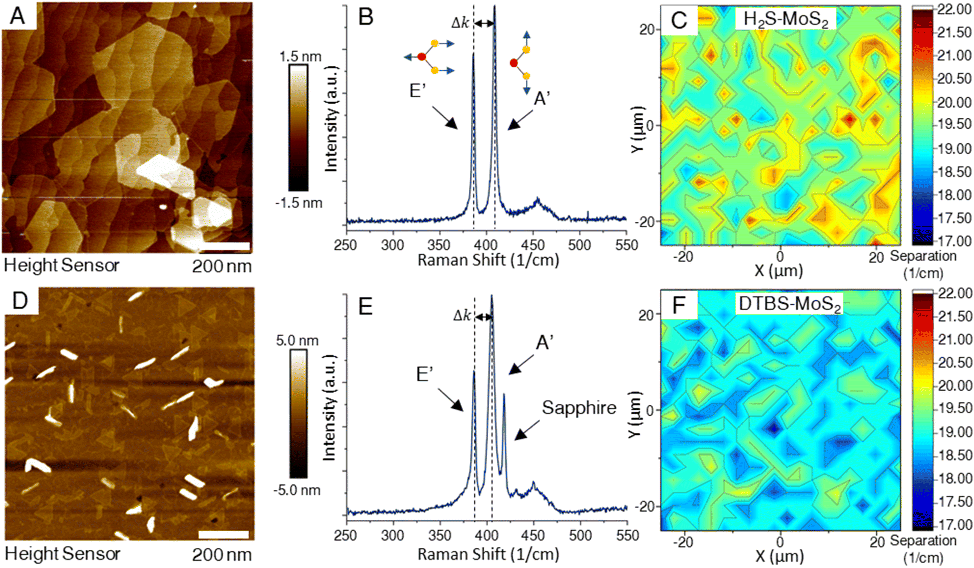 | ||
| Fig. 1 A and D) AFM topography from each sample showing bilayer and multilayer domains. The thinner linear regions are areas of out of plane growth. (B and E) Representative Raman spectra for MoS2 samples from the H2S process (top row) and the DTBS process showing (bottom row) the locations of the characteristic in-plane and out-of-plane Raman peaks. The spectrum in (E) also has a pronounced sapphire peak due to the lack of additional layers above the TMD monolayer. At low laser power additional MoS2 layers mask the sapphire signal. (C and F) 50 μm × 50 μm map of the peak separation for both H2S and DTBS, respectively. Each shows an average value near 19 (cm−1) confirming monolayer coverage. Areas of higher separation are due to multilayer growth. | ||
Image processing and analysis was performed on the AFM images using FIJI to assess the degree of monolayer, bilayer, and multilayer/out-of-plane growth for each distinct MoS2 sample. First, the images were converted to grayscale and manually segmented using histogram analysis. A binary mask of each segment was generated using an ISO data thresholding method, and the foreground pixels of each mask were divided by the total number of pixels to quantify each segment's contribution to the total image. For the H2S–MoS2, the layer coverage was estimated to be 31.37% bilayer, and 1.59% multilayer/out-of-plane (ESI Fig. 1†). While the DTBS–MoS2 estimated 15.90% bilayer coverage and 3.49% multilayer/out-of-plane growth.
3.2 Layer determination by Raman
Raman spectroscopy is a non-destructive technique that has emerged as a powerful tool to investigate the structural and electronic properties of TMDs.28–36 Raman spectroscopy is based on the inelastic scattering of light, where the difference in energy between incident and scattered photons provides information about the vibrational modes of the material under investigation. In 2D TMDs, two key Raman-active modes are typically observed – the in-plane (E′) and out-of-plane (A′) modes. The E′ mode originates from the opposite motion of metal and chalcogen atoms in the plane. The A′ mode is associated with the out-of-plane vibrations of the chalcogen atoms. These modes can be used to probe layer number, strain, and photon–phonon interactions in TMDs. Determining the number of layers in the TMD thin films can be achieved by measuring the separation between the characteristic A′ and E′ peaks. The frequency separation between these two peaks changes as the number of layers increases. In monolayer MoS2, the peak separation is less than 19 cm−1.37 As the layer number increases, the peak separation expands, eventually approaching the value characteristic of the bulk material around 24 cm−1.37,38 This peak separation results from changes in the interlayer interactions and electronic structure with added layers. By measuring the frequency difference between the E′ and A′ peaks and comparing this value to established standards for different layer numbers, one can estimate the layer count of TMD samples. In Fig. 1, Raman maps from of samples from both processes indicated high levels of layer homogeneity, with sample from the H2S process measuring a larger peak separation on the average. This is supported by AFM measurements of the samples which clearly show the large bilayer domains that form on the H2S–MoS2 samples while reaching coalescence of the monolayer. In Fig. 1E, the sapphire peak located near 418 cm−1 in the Raman spectra of the DTBS–MoS2 sample is much more pronounced due to the lack of additional layers above the monolayer. It is crucial to account for other factors like strain and doping, which can also influence the Raman peak positions and often limit the comparison to only samples with similar preparation methods.3.3 Comparative analysis of layer quality
In the context of TMDs, the presence of defects often induces changes in the position, FWHM, and intensity of the Raman peaks. Specifically, a defect-induced LA(M) Raman peak can be observed at around 227 cm−1 for MoS2 samples that are sufficiently defective.38,39 Both growth processes produced MoS2 samples of sufficient quality such that the LA(M) peak is absent in the spectra of all MoS2 samples analyzed.31Broadening of Raman peaks is often used as an indicator of structural disorder or defects, suggesting a higher defect density relative to similarly prepared samples.40,41 To gain a comparative understanding of the defect nature of the samples considered in this study, the FWHMs of the Lorentzian peaks fit to the in-plane Raman mode were compared across the two samples. Fig. 2 provides spectra and heat maps of the analyzed FWHM. The representative sample from the H2S samples had a mean value of 3.457 cm−1, which is lower than the mean value of 3.904 cm−1 measured for DTBS–MoS2. There is also a visible shouldering of this peak that does not appear in the H2S–MoS2.
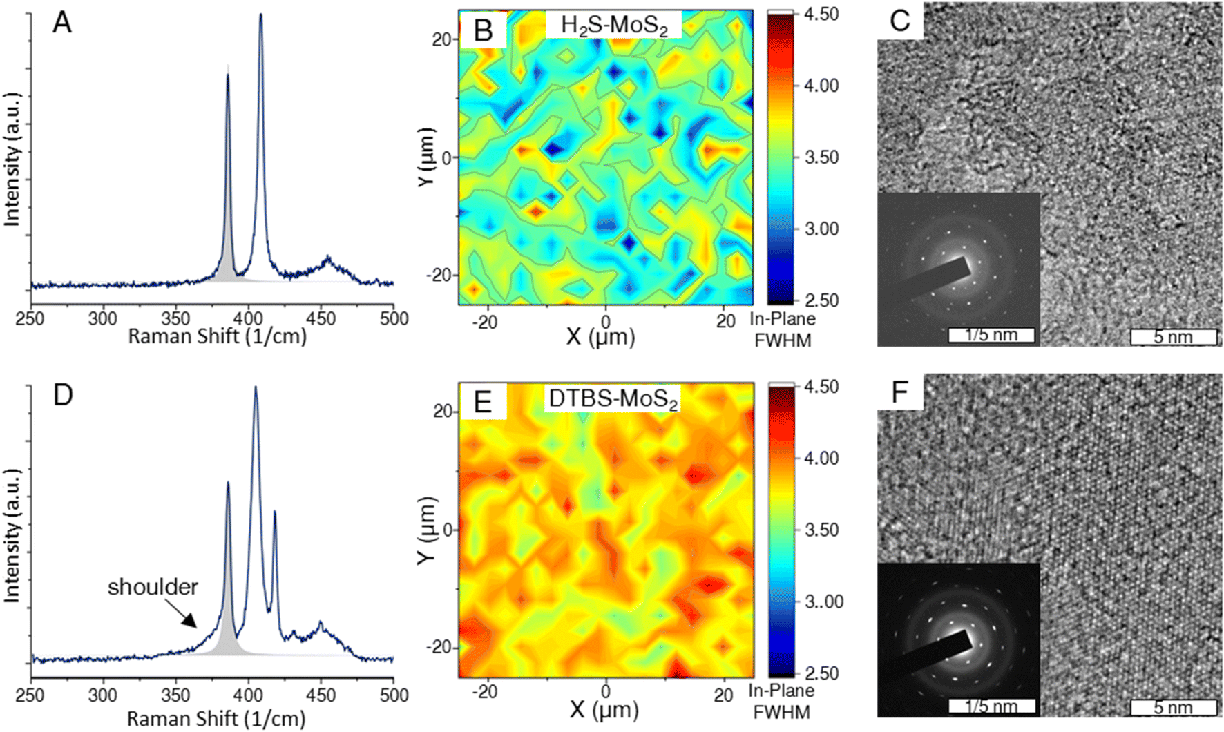 | ||
| Fig. 2 (A and D) Representative spectra of MoS2 samples from the H2S process (top row) and the DTBS process (bottom row). The shaded area represents the Lorentzian fit of the E′ peak for which the FWHM was mapped. Note that in addition to being wider, there is a left-handed shoulder on the E′ peak for DTBS samples. (B and E) 50 μm × 50 μm maps of the FWHM of the out of plane E′ peak for MoS2 samples. (C and F) Respective TEM image with accompanying diffraction pattern. | ||
We purchased a 1 cm coupon of commercially available MoS2 grown by Chemical Vapor Deposition (CVD) that advertises domain sizes of (1–50 μm) to compare Raman spectra (ESI Fig. 2†). The commercial MoS2 sample showed monolayer peak separation and a lower in-plane mode FWHM than both the experimental samples, supporting the higher advertised quality. The lack of the LA(M) peak from all spectra suggests that standard MOCVD processes are approaching the quality of commercially available material.31
TEM images provide further evidence of a difference in quality between the two differentially grown samples. While both samples are highly crystalline, as the domains grow towards coalescence, the samples grown by the H2S process appear to be more closely oriented. TMD films are known to preferentially orient according to substrate step edges under appropriate growth conditions.42,43 The purpose of the pre-growth anneal step in the horizontal reactor recipe is to enhance the sapphire terraces and domain orientation. This results in a more precise diffraction pattern shown in Fig. 2. As the orientation becomes more varied in the DTBS grown samples, the points in the diffraction pattern take on a more elliptical character. Misoriented domain edges are thought to contribute more to the defect nature of the basal plane than highly oriented coalesced domains.44
Both the Raman and TEM analysis indicate a higher defect density in the DTBS–MoS2. This is likely due to the difference in growth temperature, with a higher temperature allowing for more effective Ostwald ripening to orient crystal domains reducing grain boundary defects.45,46 The growth temperature for the DTBS recipe may limited by the carbon containing sulfur precursor di-tert-butyl sulfide, which can cause carbon contamination at increased temperatures an influence the ripening process.47,48 The use of the hydride sulfur source allows for increased growth temperature which promotes greater crystallinity but requires much more complicated safety protocols and systems. Additionally, the use of a post growth annealing step using the hydride precursor is intended to minimize sulfur vacancy point defects in the film.
3.4 XPS characterization
Survey scans of both samples (ESI Fig. 3†) reveal significantly more carbon incorporation in the DTBS process. After the initial measurement, samples were thoroughly cleaned to remove surface contaminants and remeasured yielding the same result, indicating the signal is from carbon incorporated into the layer. While both samples also contain a strong oxygen signal, due to the underlying substrate being alumina, we are unable to determine relative amounts of oxygen incorporation into the layer and elemental mapping of deposited layers is relegated to future work.3.5 Kelvin probe force microscopy
It was observed that for the two samples the contact potential difference (CPD) map had a differing correlation with the colocalized AFM topography as depicted in Fig. 3. The measurement from the H2S–MoS2 shows a high obvious contrast in the CDP map along domain edges with lower CDP values on the basal plane. For the DTBS–MoS2, this contrast does not appear, even when isolating clearly defined bilayer domains. It is suspected that the qualitative difference in the KFPM measurements of the two the differently grown samples is due to the difference in the defect nature of the films with defects such as vacancies or grain boundaries altering the surface energy landscape of the film. XPS results indicate significantly more carbon incorporation in the DTBS–MoS2 films. Carbon impurities, and impurities in general, are expected to bond more preferentially to defect sites over the basal plane. Lastly, a possible explanation for this is that ambient doping (oxidization) is expected to occur at a higher rate at defect sites for TMD materials.49–51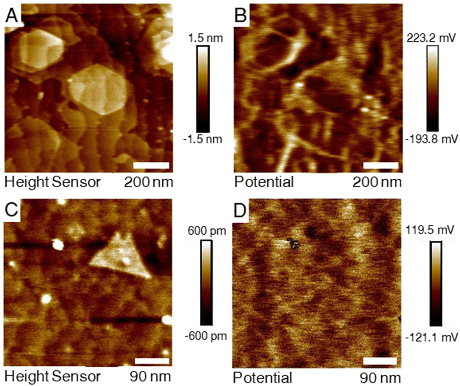 | ||
| Fig. 3 (A and B) Colocalized AFM topography and KPFM contact potential difference maps for a sample that was grown by the H2S process (top row). Brighter areas, indicating an increased potential difference, correlate to domain edges. (C and D) The same maps for a sample from the DTBS process (bottom row). For this sample, the map was oriented on an isolated triangular bilayer domain and was reduced in size to avoid out of plane growth regions that would have interfered with the required lift height. The CPD map shows no meaningful correlation to the respective topography. | ||
3.6 Sheet resistivity
The 4-point measurements conducted on the printed devices shown in Fig. 4 resulted in a sheet resistivity measurement for the DTBS grown samples that was nearly 2.5 times lower than that of the samples grown utilizing H2S. The sheet resistivity for the DTBS grown material-based devices were 1.31 MΩ per square, with the H2S based devices measuring 3.4 MΩ per square. It has been reported that spontaneous oxygen doping of MoS2 films in atmosphere can lower their sheet resistivity.52 Other impurities, possibly due to incomplete decomposition of precursors could also explain this difference in resistivity.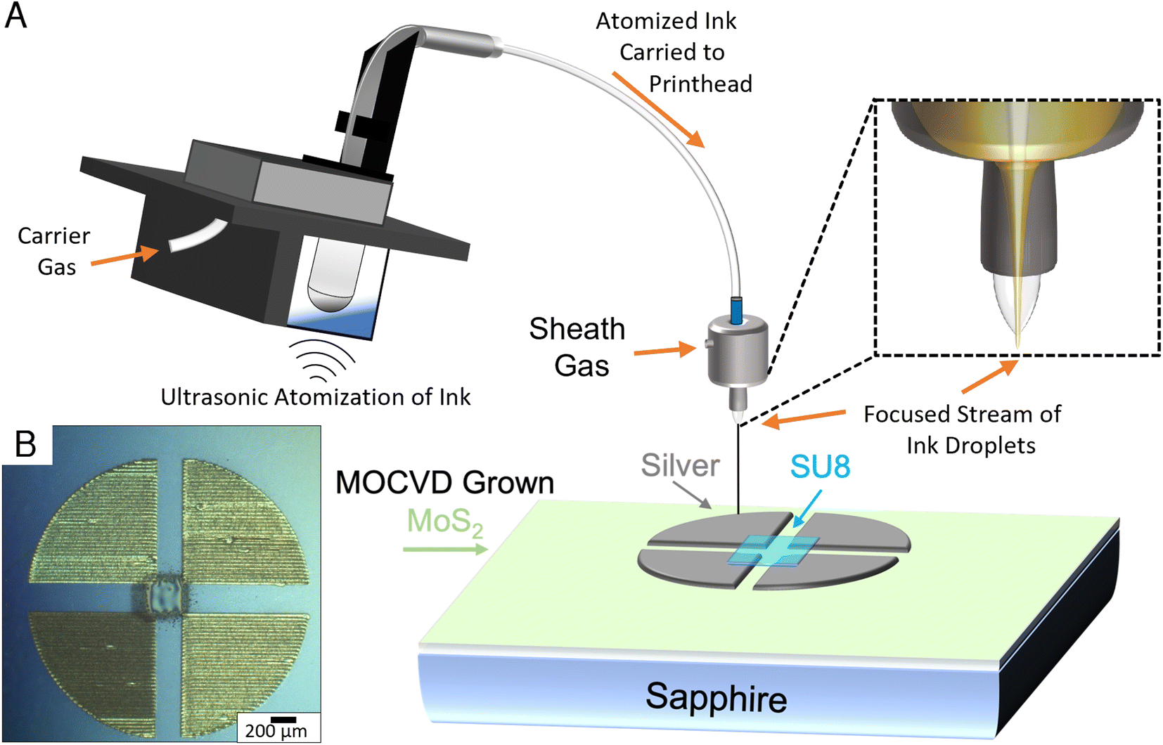 | ||
| Fig. 4 (A) Cartoon schematic illustrating the aerosol jet printing process and the deposition of a silver van der Pauw 4-point device with a printed SU-8 passivation region on MOCVD MoS2. (B) Optical microscope image of the AJ-printed device after curing of SU-8 and removal of excess TMD material. | ||
4. Conclusion
The correlation of traditional TMD characterization results with qualitative electrical measurements was investigated for two sets of samples with differing growth conditions. The coalesced wafer scale samples were prepared using an organosulfide precursor and a hydride precursor that resulted in differing surface topography and defect nature of the films. Monolayers deposited using the H2S appeared to be less defective likely due to the higher growth temperature enabled by a carbon lacking sulfur precursor. However, use of H2S as a precursor requires significantly enhanced safety protocols. The defect nature of the films correlated with maps of the contact potential difference, where samples of higher crystal quality showed higher contrast between grain edges and domain basal planes. This contrast is thought to be caused by surface energy variations due to differing defect distributions in the monolayers or by varying amount impurity incorporation, such as carbon or oxygen either from precursor selection or spontaneous ambient doping. By using KFPM and aerosol jet printing on the growth substate, the energy landscape of these monolayers as able to be assessed rapidly without fabrication or transfer.Data availability
The data supporting this article have been included in the manuscript and as part of the ESI.†Author contributions
D. E. and M. C. conceived the experiments. M. C. participated in the growths of the H2S–MoS2 with C. C. as part of the 2D Crystal Consortium Resident Scholar Visitor Program (RSVP) under the supervision of J. R. S. P. conducted the growths using DTBS under the supervision of S. E. O. M. conducted the KPFM measurement. N. M. printed the VDP test structures and led the electrical characterization. K. C. performed the TEM imaging and interpreted the results. J. E. conducted XPS measurements. M. C. performed data analysis and interpreted the results with input from all authors. M. C. wrote the original manuscript and revised it with input from all authors.Conflicts of interest
The authors declare no competing financial interests.Acknowledgements
This material is based upon work supported under a University Nuclear Leadership Program Graduate Fellowship. The authors acknowledge infrastructure support from the Department of Energy Nuclear Science User Facilities General Infrastructure Program through award numbers DE-NE0008677 and DE-NE0008496. Any opinions, findings, conclusions or recommendations expressed in this publication are those of the author(s) and do not necessarily reflect the views of the Department of Energy Office of Nuclear Energy. The H2S MoS2 samples were grown in the 2D Crystal Consortium-Materials Innovation Platform (2DCC-MIP) facility, which is supported by the National Science Foundation under cooperative agreement NSF DMR-2039351. D. E. and M. C. acknowledge helpful discussion with Jason Lynch and Deep Jariwala at the University of Pennsylvania, as well as with Katie Nielson and Eric Pop at Stanford University. This work was supported in part by the Air Force Research Laboratory (AFRL) under Agreement Number FA8650-20-2-5506. The U.S. Government is authorized to reproduce and distribute reprints for Governmental Purposes, notwithstanding any copyright notation thereon.References
- Y. Shi, B. Groven, J. Serron, X. Wu, A. N. Mehta, A. Minj, S. Sergeant, H. Han, I. Asselberghs, D. Lin, S. Brems, C. Huyghebaert, P. Morin, I. Radu and M. Caymax, ACS Nano, 2021, 15, 9482–9494 CrossRef CAS PubMed.
- D. Reifsnyder Hickey, N. Nayir, M. Chubarov, T. H. Choudhury, S. Bachu, L. Miao, Y. Wang, C. Qian, V. H. Crespi, J. M. Redwing, A. C. T. van Duin and N. Alem, Nano Lett., 2021, 21, 6487–6495 CrossRef CAS PubMed.
- P. Yang, D. Wang, X. Zhao, W. Quan, Q. Jiang, X. Li, B. Tang, J. Hu, L. Zhu, S. Pan, Y. Shi, Y. Huan, F. Cui, S. Qiao, Q. Chen, Z. Liu, X. Zou and Y. Zhang, Nat. Commun., 2022, 13, 3238 CrossRef CAS PubMed.
- P. Zheng, W. Wei, Z. Liang, B. Qin, J. Tian, J. Wang, R. Qiao, Y. Ren, J. Chen, C. Huang, X. Zhou, G. Zhang, Z. Tang, D. Yu, F. Ding, K. Liu and X. Xu, Nat. Commun., 2023, 14, 592 CrossRef CAS PubMed.
- L. Liu, T. Li, L. Ma, W. Li, S. Gao, W. Sun, R. Dong, X. Zou, D. Fan, L. Shao, C. Gu, N. Dai, Z. Yu, X. Chen, X. Tu, Y. Nie, P. Wang, J. Wang, Y. Shi and X. Wang, Nature, 2022, 605, 69–75 CrossRef CAS PubMed.
- T. Li, W. Guo, L. Ma, W. Li, Z. Yu, Z. Han, S. Gao, L. Liu, D. Fan, Z. Wang, Y. Yang, W. Lin, Z. Luo, X. Chen, N. Dai, X. Tu, D. Pan, Y. Yao, P. Wang, Y. Nie, J. Wang, Y. Shi and X. Wang, Nat. Nanotechnol., 2021, 16, 1201–1207 CrossRef CAS PubMed.
- P. Yang, S. Zhang, S. Pan, B. Tang, Y. Liang, X. Zhao, Z. Zhang, J. Shi, Y. Huan, Y. Shi, S. J. Pennycook, Z. Ren, G. Zhang, Q. Chen, X. Zou, Z. Liu and Y. Zhang, ACS Nano, 2020, 14, 5036–5045 CrossRef CAS PubMed.
- J.-H. Fu, J. Min, C.-K. Chang, C.-C. Tseng, Q. Wang, H. Sugisaki, C. Li, Y.-M. Chang, I. Alnami, W.-R. Syong, C. Lin, F. Fang, L. Zhao, T.-H. Lo, C.-S. Lai, W.-S. Chiu, Z.-S. Jian, W.-H. Chang, Y.-J. Lu, K. Shih, L.-J. Li, Y. Wan, Y. Shi and V. Tung, Nat. Nanotechnol., 2023, 18, 1289–1294 CrossRef CAS.
- H. Zhu, N. Nayir, T. H. Choudhury, A. Bansal, B. Huet, K. Zhang, A. A. Puretzky, S. Bachu, K. York, T. V. Mc Knight, N. Trainor, A. Oberoi, K. Wang, S. Das, R. A. Makin, S. M. Durbin, S. Huang, N. Alem, V. H. Crespi, A. C. T. van Duin and J. M. Redwing, Nat. Nanotechnol., 2023, 18, 1295–1302 CrossRef CAS PubMed.
- L. Liu and J. H. Edgar, Mater. Sci. Eng., R, 2002, 37, 61–127 CrossRef.
- R. D. Dupuis, Science, 1984, 226, 623–629 CrossRef CAS.
- S. Nakamura, T. Mukai, M. S. M. Senoh and N. I. N. Iwasa, Jpn. J. Appl. Phys., 1992, 31, L139 CrossRef CAS.
- H. M. Manasevit, J. Cryst. Growth, 1972, 13–14, 306–314 Search PubMed.
- Q. H. Wang, K. Kalantar-Zadeh, A. Kis, J. N. Coleman and M. S. Strano, Nat. Nanotechnol., 2012, 7, 699–712 Search PubMed.
- J. A. Wilson and A. D. Yoffe, Adv. Phys., 1969, 18, 193–335 Search PubMed.
- K. S. Novoselov, D. Jiang, F. Schedin, T. J. Booth, V. V. Khotkevich, S. V. Morozov and A. K. Geim, Proc. Natl. Acad. Sci. U. S. A., 2005, 102, 10451–10453 CrossRef CAS.
- K. S. Novoselov, A. K. Geim, S. V. Morozov, D. Jiang, Y. Zhang, S. V. Dubonos, I. V. Grigorieva and A. A. Firsov, Science, 2004, 306, 666–669 CrossRef CAS PubMed.
- K. F. Mak, C. Lee, J. Hone, J. Shan and T. F. Heinz, Phys. Rev. Lett., 2010, 105, 136805 CrossRef PubMed.
- K. F. Mak, C. Lee, J. Hone, J. Shan and T. F. Heinz, Phys. Rev. Lett., 2010, 105, 136805 CrossRef.
- M. Chhowalla, H. S. Shin, G. Eda, L. J. Li, K. P. Loh and H. Zhang, Nat. Chem., 2013, 5, 263–275 CrossRef PubMed.
- Y. H. Lee, X. Q. Zhang, W. Zhang, M. T. Chang, C. T. Lin, K. D. Chang, Y. C. Yu, J. T. W. Wang, C. S. Chang, L. J. Li and T. W. Lin, Adv. Mater., 2012, 24, 2320–2325 CrossRef CAS PubMed.
- K. Momeni, Y. Ji, N. Nayir, N. Sakib, H. Zhu, S. Paul, T. H. Choudhury, S. Neshani, A. C. T. van Duin, J. M. Redwing and L. Q. Chen, npj Comput. Mater., 2022, 8, 240 CrossRef CAS.
- Monolayer MoS2 Grown by MOCVD on Sapphire for Reactor Comparison Study [Data Set], ed. C. Chen and J. Redwing, 2023 Search PubMed.
- K. T. Fujimoto, J. K. Watkins, T. Phero, D. Litteken, K. Tsai, T. Bingham, K. L. Ranganatha, B. C. Johnson, Z. Deng, B. Jaques and D. Estrada, npj Flexible Electron., 2020, 4, 32 CrossRef.
- T. L. Phero, K. A. Novich, B. C. Johnson, M. D. McMurtrey, D. Estrada and B. J. Jaques, Sens. Actuators, A, 2022, 344, 113691 CrossRef CAS.
- N. McKibben, B. Ryel, J. Manzi, F. Muramutsa, J. Daw, H. Subbaraman, D. Estrada and Z. Deng, Microsyst. Nanoeng., 2023, 9, 51 CrossRef CAS PubMed.
- J.-H. Park, A.-Y. Lu, P.-C. Shen, B. G. Shin, H. Wang, N. Mao, R. Xu, S. J. Jung, D. Ham, K. Kern, Y. Han and J. Kong, Small Methods, 2021, 5, 2000720 CrossRef CAS.
- C. Lee, H. Yan, L. E. Brus, T. F. Heinz, J. Hone and S. Ryu, ACS Nano, 2010, 4, 2695–2700 CrossRef CAS PubMed.
- S. Mignuzzi, A. J. Pollard, N. Bonini, B. Brennan, I. S. Gilmore, M. A. Pimenta, D. Richards and D. Roy, Phys. Rev. B: Condens. Matter Mater. Phys., 2015, 91, 195411 CrossRef.
- H. J. Kim, D. Kim, S. Jung, M. H. Bae, Y. J. Yun, S. N. Yi, J. S. Yu, J. H. Kim and D. H. Ha, J. Raman Spectrosc., 2018, 49, 1938–1944 CrossRef CAS.
- R. N. Gontijo, T. Zhang, K. Fujisawa, A. L. Elías, M. A. Pimenta, A. Righi, M. Terrones and C. Fantini, 2D Mater., 2021, 8, 035042 CrossRef CAS.
- Z. Kou, A. Hashemi, M. J. Puska, A. V. Krasheninnikov and H. P. Komsa, npj Comput. Mater., 2020, 6, 1–7 CrossRef.
- M. A. Pimenta, E. Del Corro, B. R. Carvalho, C. Fantini and L. M. Malard, Acc. Chem. Res., 2015, 48, 41–47 CrossRef CAS.
- H. J. Conley, B. Wang, J. I. Ziegler, R. F. Haglund, S. T. Pantelides and K. I. Bolotin, Nano Lett., 2013, 13, 3626–3630 CrossRef CAS PubMed.
- Y. Wang, C. Cong, C. Qiu and T. Yu, Small, 2013, 9, 2857–2861 CrossRef CAS PubMed.
- X. Zhang, W. P. Han, J. B. Wu, S. Milana, Y. Lu, Q. Q. Li, A. C. Ferrari and P. H. Tan, Phys. Rev. B: Condens. Matter Mater. Phys., 2013, 87, 1–8 Search PubMed.
- H. Li, Q. Zhang, C. C. R. Yap, B. K. Tay, T. H. T. Edwin, A. Olivier and D. Baillargeat, Adv. Funct. Mater., 2012, 22, 1385–1390 CrossRef CAS.
- A. Berkdemir, H. R. Gutiérrez, A. R. Botello-Méndez, N. Perea-López, A. L. Elías, C. I. Chia, B. Wang, V. H. Crespi, F. López-Urías, J. C. Charlier, H. Terrones and M. Terrones, Sci. Rep., 2013, 3, 1–8 Search PubMed.
- S. Mignuzzi, A. J. Pollard, N. Bonini, B. Brennan, I. S. Gilmore, M. A. Pimenta, D. Richards and D. Roy, Phys. Rev. B: Condens. Matter Mater. Phys., 2015, 91, 195411 CrossRef.
- H. Cun, M. Macha, H. K. Kim, K. Liu, Y. Zhao, T. LaGrange, A. Kis and A. Radenovic, Nano Res., 2019, 12, 2646–2652 CrossRef CAS.
- H. Yu, M. Liao, W. Zhao, G. Liu, X. J. Zhou, Z. Wei, X. Xu, K. Liu, Z. Hu, K. Deng, S. Zhou, J. A. Shi, L. Gu, C. Shen, T. Zhang, L. Du, L. Xie, J. Zhu, W. Chen, R. Yang, D. Shi and G. Zhang, ACS Nano, 2017, 11, 12001–12007 CrossRef CAS PubMed.
- J. You, M. D. Hossain and Z. Luo, Nano Convergence, 2018, 5, 26 CrossRef.
- Y. Shi, B. Groven, J. Serron, X. Wu, A. N. Mehta, A. Minj, S. Sergeant, H. Han, I. Asselberghs, D. Lin, S. Brems, C. Huyghebaert, P. Morin, I. Radu and M. Caymax, ACS Nano, 2021, 15, 9482–9494 CrossRef CAS PubMed.
- T. H. Ly, D. J. Perello, J. Zhao, Q. Deng, H. Kim, G. H. Han, S. H. Chae, H. Y. Jeong and Y. H. Lee, Nat. Commun., 2016, 7, 10426 CrossRef CAS PubMed.
- M. Liu, J. Liao, Y. Liu, L. Li, R. Wen, T. Hou, R. Ji, K. Wang, Z. Xing, D. Zheng, J. Yuan, F. Hu, Y. Tian, X. Wang, Y. Zhang, A. Bachmatiuk, M. H. Rümmeli, R. Zuo and Y. Hao, Adv. Funct. Mater., 2023, 33, 2212773 CrossRef CAS.
- G. Madras and B. J. McCoy, J. Chem. Phys., 2003, 119, 1683–1693 CrossRef CAS.
- R. K. Lindsey, N. Goldman, L. E. Fried and S. Bastea, Nat. Commun., 2022, 13, 1424 CrossRef CAS PubMed.
- C. M. Schaefer, J. M. C. Roque, G. Sauthier, J. Bousquet, C. Hébert, J. R. Sperling, A. Pérez-Tomás, J. Santiso, E. Del Corro and J. A. Garrido, Chem. Mater., 2021, 33, 4474–4487 CrossRef CAS.
- S. Kc, R. Longo, R. Wallace and K. Cho, J. Appl. Phys., 2015, 117, 135301 CrossRef.
- J. Gao, B. Li, J. Tan, P. Chow, T. M. Lu and N. Koratkar, ACS Nano, 2016, 10, 2628–2635 CrossRef CAS PubMed.
- J. Pető, T. Ollár, P. Vancsó, Z. I. Popov, G. Z. Magda, G. Dobrik, C. Hwang, P. B. Sorokin and L. Tapasztó, Nat. Chem., 2018, 10, 1246–1251 CrossRef PubMed.
- J. Tang, Z. Wei, Q. Wang, Y. Wang, B. Han, X. Li, B. Huang, M. Liao, J. Liu, N. Li, Y. Zhao, C. Shen, Y. Guo, X. Bai, P. Gao, W. Yang, L. Chen, K. Wu, R. Yang, D. Shi and G. Zhang, Small, 2020, 16, 2004276 CrossRef CAS PubMed.
Footnote |
| † Electronic supplementary information (ESI) available. See DOI: https://doi.org/10.1039/d4ra04279d |
| This journal is © The Royal Society of Chemistry 2024 |