DOI:
10.1039/D4RA04249B
(Paper)
RSC Adv., 2024,
14, 29439-29454
Electrodeposition of Cu2NiSnS4 absorber layer on FTO substrate for solar cell applications
Received
10th June 2024
, Accepted 28th August 2024
First published on 18th September 2024
Abstract
Potentiostatic and in situ electrochemical impedance spectroscopy (EIS) measurements were recorded to study the nucleation and growth mechanisms of electrodeposited Cu2NiSnS4 (CNTS) thin films from aqueous solution at different applied potentials. The electrodeposition process of Cu–Ni–Sn–S precursors were studied using cyclic voltammetry and chronoamperometry techniques. The nucleation and growth mechanism of these films was found to follow a three-dimensional progressive nucleation limited by diffusion-controlled growth. The nucleation mechanism is found to be influenced by the presence of S2O32−, which prompts the electrodeposition of S. In situ electrochemical impedance spectroscopy (EIS) investigates the electrodeposition behavior of CNTS precursors on the surface electrode. A capacitive behavior was observed at high frequencies, while the presence of Warburg diffusion was detected only for potentials less negative than −1.0 V vs. Ag/AgCl. The crystallographic structure, morphology, composition, and optical band gap of CNTS thin films was examined using X-ray diffraction, Raman spectroscopy, scanning electron microscopy, and UV-visible spectroscopy. Electrodeposition at −0.98 V vs. Ag/AgCl resulted in the formation of microsheets with a uniform morphology and homogeneous thickness of sulfurized CNTS film. This potential also proved to be optimal for achieving higher crystallinity, a pure phase, and a suitable band gap energy of approximately 1.6 eV.
1. Introduction
A great deal of work has been devoted to the production of Cu(In,Ga)Se2 and CdTe-based solar cells, due to their excellent optical properties and high efficiency. However, the use of toxic heavy metals restricts the applicability and marketability of these cells. Consequently, research focus has shifted towards quaternary chalcopyrites naturally abundant on Earth, such as Cu2XSnS4 (where X represents Zn, Fe, Co, or Ni). In particular, there has been considerable interest in the development of solar cells utilizing Cu2ZnSnS4 (CZTS) as a foundational material.1–3 It has a linearly optimal direct band energy of 1.4 to 1.6 eV, a high absorption coefficient of 4 × 104 cm−1, and a theoretical power energy conversion (PEC) limit of 32.2%. In practice, PEC of CZTS has grown rapidly, initially from 0.66% (ref. 4 and 5) to over 13%.6 Cu2FeSnS4 (CFTS) absorbs strongly at a visible wavelength with a shift of about 1.5 eV. Yan et al.7 have fabricated CFTS nanocrystals that exhibit a stable photoelectrochemical response using the hot injection method. Zhang et al. have developed a colloidal method for the synthesis of Cu2CoSnS4 (CCTS) nanocrystals in the vortex phase, based on the dissolution process.8 Cu2NiSnS4 (CNTS) was identified as one of the most promising candidates due to its direct band gap and high absorption coefficient. Kamble et al. used the hot injection method to prepare wurtzite-type CNTS nanoparticles.9 Similarly, Wang et al. used a solvothermal method to synthesize CNTS nanoparticles with a flower-like structure.10 Sarkar and colleagues opted for hydrothermal synthesis of CNTS nanoparticles, generating a favorable photo-response.11 CNTS has also been elevated to counter-electrode status in dye-sensitized solar cells. Xie and colleagues12 examined the replacement of Zn2+ in CZTS materials, demonstrating that Cu2MnSnS4 and Cu2NiSnS4 counter electrodes outperform Pt in DSSCs using ZnO as the base material. Several methods have been employed to create carbon CNTS based quaternary compounds, including solvothermal techniques,12 spin coating,13 spray pyrolysis,14 and electrodeposition.15–18 Among these techniques, the latter has recently received considerable attention due to its comparatively simple and inexpensive process compared to other methods such as physical vapor deposition (PVD) or chemical vapor deposition (CVD). In addition, it shows potential for high-volume production of thin films containing quaternary compounds.
Studying the mechanisms of nucleation and growth through electrochemical techniques is highly advantageous. These methods facilitate the analysis, control, and measurement of parameters such as current, electrode potential, and charge. Consequently, they allow for the manipulation of supersaturation (overpotential) within the system, thus influencing the conditions for the development of new phases from the nanoscale to the microscale.19–21
There are few reports available concerning the electrodeposition process for the creation of CNTS thin films. These studies employed a single-step electrodeposition method to successfully produce Cu2NiSnS4 thin films, featuring a pure stannite phase.15,22–24 Additionally, this research focuses primarily on the electrochemical properties of CNTS thin films, neglecting the electrochemical mechanism. The mechanism of electrochemical, including the nucleation and growth processes of the deposited layer, exerts a significant influence on the electrodeposition process. The electrochemical kinetics of CNTS electrodeposition can also be affected by various factors, such as the deposition potential, bulk composition, temperature bath, and electrode material. However, to date, we are not aware of any literature or in-depth study that addresses these issues.
In this study, CNTS were electrodeposited from a sulfate solution. The nucleation and growth mechanisms of Cu–Ni–Sn–S were systematically investigated. Additionally, the diffusion coefficient (D) was calculated, the effect of S2O32− on the electrochemical behavior of cations was examined, and the impact of deposition potential on the surface morphology of the CNTS layer was studied.
2. Experimental
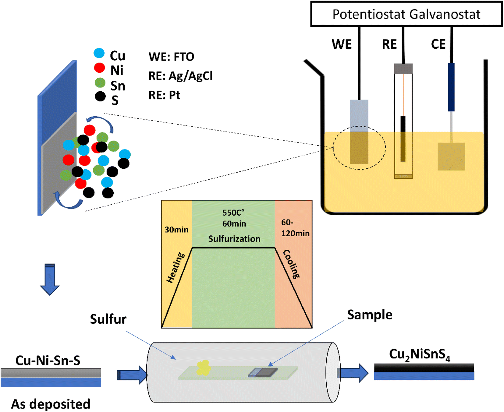
CNTS films were deposited by co-electrodeposition on an FTO coated glass electrode from a 50 ml of solution consisting of 0.025 M NiSO4·6H2O, 0.02 M CuSO4·5H2O, 0.015 M SnSO4, and 0.02 M Na2S2O3 as the precursor for the electrodeposition of Cu–Ni–Sn–S. Additionally, 0.1 M Na3C6H5O7 was employed as the supporting electrolyte. This final reagent served as a complexing agent to reduce the reduction potential differences between the cations and to maintain the electrolyte pH at approximately 5.5. All chemicals were used as received without further purification. The electrodeposition process was carried out using a three-electrode cell with a VersaSTAT 3 potentiostat. A platinum plate served as the counter-electrode (CE) to measure the resultant current. About 0.45 cm2 surface of fluorine-doped tin oxide (FTO) substrate, characterized by its transparent conductive properties, was utilized as the substrate for thin film deposition. This material features a substrate thickness of 2.2 mm, a resistivity ranging from 7 to 10 Ω □−1, and a transmittance exceeding 80%. Due to its excellent conductivity and optical transparency, FTO is widely employed in various electronic applications, including solar cells. An Ag/AgCl/KCl electrode was employed as the reference electrode (RE) to precisely control the potential applied to the working electrode. The distance between the working and reference electrodes was approximately 1 cm to ensure accurate potential control, while the counter electrode was placed approximately 1.5 cm away from the working electrode to provide sufficient separation and minimize interference. The cell was designed to allow for efficient mixing and uniform distribution of the electrolyte, ensuring consistent mass transport conditions (Fig. 1). The cyclic voltammetry (CV) was conducted to investigate the electrochemical behavior of the elements. Chronoamperometry (CA) was used to monitor the electrodeposition process and study the mechanism. Finally, the investigation of Electrochemical Impedance Spectroscopy (EIS) was carried out using the same cell electrolyte. A 10 mV amplitude excitation signal was applied to record the EIS spectra within the frequency range of 100 kHz to 1 mHz, maintaining the same potential as the accumulation potential during the co-electrodeposition of Cu–Ni–Sn–S.
 |
| | Fig. 1 Schematic representation of the fabrication performance of CNTS thin films. | |
To achieve the desired structure of CNTS, the films were annealed in a sulfur-rich environment at a temperature of 550 °C for 1 hour. The electrochemical and sulfurization process are represented schematically in Fig. 1.
The crystallinity of the samples was assessed with high-resolution X-ray diffraction using Cu-Kα radiation (wavelength 1.5418 Å). Raman spectroscopy was employed to confirm the crystalline phases of the samples. The measurements were conducted using a Raman spectrometer equipped with a microscope and a He–Ne laser operating at an excitation wavelength of 633 nm. The spectrometer was configured to operate within a wavenumber range of 100 cm−1 to 500 cm−1. The CNTS morphology was characterized by field emission scanning electron microscopy (SEM). Chemical composition and mapping were analyzed by Energy Dispersive X-ray Spectroscopy (EDX) coupled with FE-SEM. Optical characteristics were analyzed using a UV spectrophotometer (Shimadzu UV-2600) over the wavelength range of 500 nm to 1400 nm.
3. Results and discussion
3.1. Electrochemical studies
3.1.1 Cyclic voltammetry. Fig. 2 presents the electrochemical behaviors of the CNTS precursor in a bath electrolyte of Na3C6H5O7 (0.1 M). Cyclic voltammetry (CV) is an electrochemical technique used to study the electrochemical properties of materials. It determines suitable potentials for the electrodeposition of thin films by sweeping the potential of a working electrode in a solution and measuring the resulting current. This method identifies reduction and oxidation reactions, providing information on the electrochemical behavior of materials and the optimal conditions for their deposition. Generally, to deposit a metallic element, a reduction potential is applied within the cathodic peak values, meaning a cathodic potential.
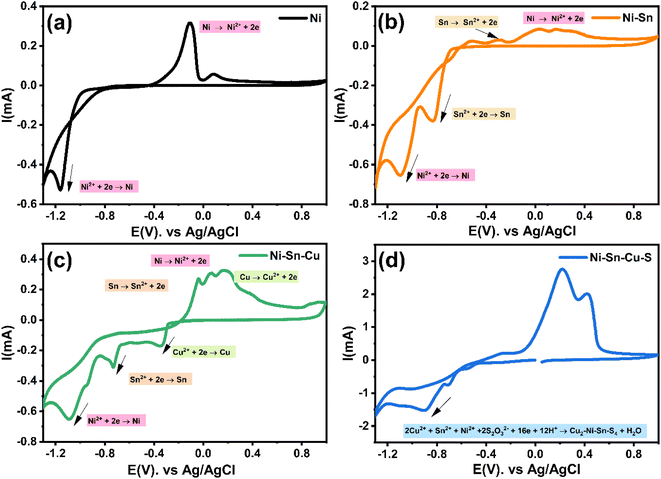 |
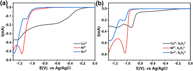
| | Fig. 2 Cyclic voltammograms of CNTS precursor in bath electrolytic containing Na3C6H5O7: (a) Ni2+ (0.035 M), (b) Ni2+ (0.035 M) + Sn2+ (0.015 M), (c) Ni2+ (0.035 M) + Sn2+ (0.015 M) + Cu2+ (0.02 M) and (d) Ni2+ (0.035 M) + Sn2+ (0.015 M) + S2O32− (0.02 M). Scan rate (25 mV s−1), potential range (1 to −1.3 V. vs. Ag/AgCl), pH = 5.5. | |
The cyclic voltammetry CV was investigated in the range of −1.3 to 1 V vs. Ag/AgCl. The Ni2+ voltammogram (Fig. 2a) displays a cathodic peak starting at −1.0 V attributed to the reduction of Ni2+ (eqn (1)) and might also be accompanied by the hydrogen evolution reaction (eqn (7)). The introduction of Sn2+ elements show the presence of a peak cathodic at −0.8 V corresponding to the Sn2+ reduction (eqn (2)) (Fig. 2b). Subsequently, the addition of Cu2+ ions to the solution results in the observation of a peak at −0.3 V, attributed to the reduction of Cu2+ ions (eqn (3)) (Fig. 2c). Following this, the S2O32− ion was added to the bulk electrolyte. Fig. 2d shows a wide, large peak around −0.9 V. This notable change can be attributed to the chemical reactions occurring between S2O32− and cations. Fig. 3a and b shows the cathodic process of Cu2+, Ni2+ and Sn2+ in presence and absence of S2O32−. It was clear that the addition of S2O32− shifted the potential peaks to the positive values. This could be attributed to the electrodeposition of sulfur (S) (eqn (4)–(6)), induced by the presence of metal ions. On the other hand, there is a significant difference between the potential peaks of the elements shown in Fig. 3a and the peaks of the same elements shown in Fig. 2a–c. This can be explained by the complexing effect of Na3C6H5O7, which decreases when the elements are in the same bath but increases when the elements are analyzed separately. The mechanism of CNTS precursor electrodeposition is believed as below.
| |
 | (1) |
| |
 | (2) |
| |
 | (3) |
| |
 | (4) |
where
ECu,
ENi, and
ESn are the Nernst potentials for the respective half-reactions relative to the Ag/AgCl reference electrode. [Cu
2+], [Ni
2+], and [Sn
2+] represent the concentrations of the respective ions in the electrolyte.
T,
F, and
R denote the temperature in kelvin, the Faraday constant, and the ideal gas constant, respectively.
25 According to the Nernst equations provided, the standard electrode potentials are −0.44 V for Ni, −0.384 V for Sn, 0.14 V for Cu, and 0.5 V for S. These values illustrate significant differences in the standard reduction potentials among Cu, Ni, Sn, and S.
| | |
2Cu2+ + Ni2+ + Sn2+ + 2S2O32− + 16e− + 12H+ → Cu2–Ni–Sn–S4 + 6H2O
| (6) |
 |
| | Fig. 3 Cathodic polarization curves of CNT precursor on FTO electrode in the electrolytic bath containing Na3C6H5O7 under the following conditions: (a) without S2O32−, (b) with S2O32−, rate scan (25 mV s−1), potential range (0 V to −1.3 V. vs. Ag/AgCl), pH = 5.5. | |
Fig. 4a shows the CV resulted from the bulk electrolyte containing the CNTS precursor at different scan rates. All plots show cathodic and anodic peaks consistent with those shown in Fig. 2d. In addition, the peaks show an increase in current intensity as the scan rate increases. Fig. 4b shows the anodic current peaks (Ipeak) around −1 V plotted as a function of the square root of the scan rate (v1/2). A robust linear correlation (R2 = 0.9917) is observed between v1/2 and Ipeak. This suggests that the limitation of the CNTS precursor deposition process on the FTO electrode surface is controlled by diffusion.
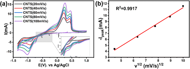 |
| | Fig. 4 (a) Cyclic voltammograms of CNTS precursor on FTO electrode at different scan rate, (b) linear plots of cathodic peak (Ipeak) current as a function of the square root of scan rate (v1/2). | |
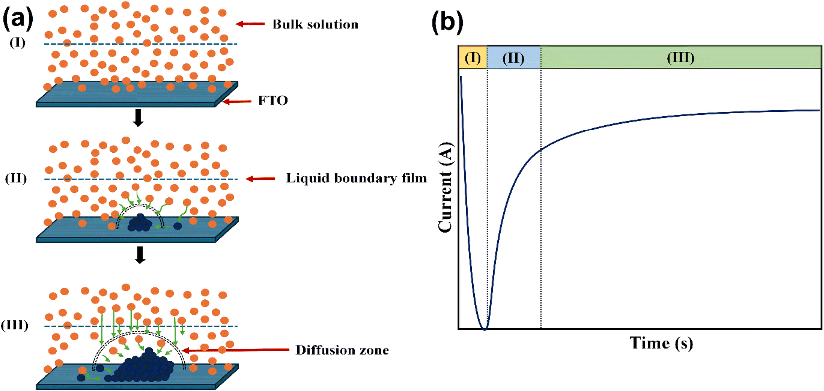
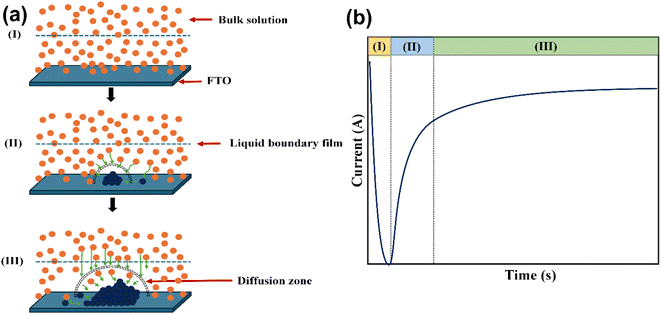
3.1.2 Chronoamperometry. Chronoamperometry (CA) is an experiment where the potential is fixed and the resulting current at the working electrode is recorded.26 The electrode current observed over time varies as an analyte diffuses from the bulk solution to the sensor surface.1 Furthermore, CA can also be used to study the nucleation and growth mechanism of the elements.27,28 Fig. 5a presents the current transients of CNT precursor onto FTO surface. The applied potential was selected according to the cathodic peak of each element, as depicted in Fig. 3a, resulting in values of −0.62 V, −1.1 V, and −1.05 V vs. Ag/AgCl for Cu2+, Ni2+, and Sn2+, respectively. As presented by the schematic view of nucleation and growth mechanism in Fig. 6a, the current transient plot (Fig. 6b) shows three distinct regions. In region (I), corresponding to the initial stage prior to potential application, a liquid boundary layer forms between the solid substrate and the bulk solution, as shown in the diagram. Region (II) is characterized by a rapid increase in current density due to metal nucleation and an increase in nucleus density. Here, electroactive species are transported to surface-formed nuclei through hemispherical diffusion zones developed around each nucleus.29 In addition, the radius of the hemispherical diffusion zones increases with time due to growth, resulting in a decrease in current density due to a decrease in the mass flux moving toward the electrode surface within region (II). In region (III) a stabilization plateau characterized by a lower current density was observed, indicating saturated growth. Clearly, for the electrodeposition of Cu, Ni and Sn, the shape of the current shows in Fig. 5 represents a typical characteristic of electrochemical nucleation and growth process. Furthermore, all transients exhibit a similar behavior, characterized by a rapid increase in current corresponding to the isolated growth of each individual copper nucleus and the increasing number of these nuclei present on the electrode surface, during which the transport of electroactive species to the nuclei formed on the surface occurs through hemispherical diffusion zones developed around each individual nucleus. As these nuclei grow, coalescence of adjacent diffusion zones with localized hemispherical nuclei results in a current maximum (Imax) followed by a decaying current, associated with diffusion-limited growth.30 These characteristics align with the nucleation of 3D hemispherical clusters followed by diffusion-limited growth.30
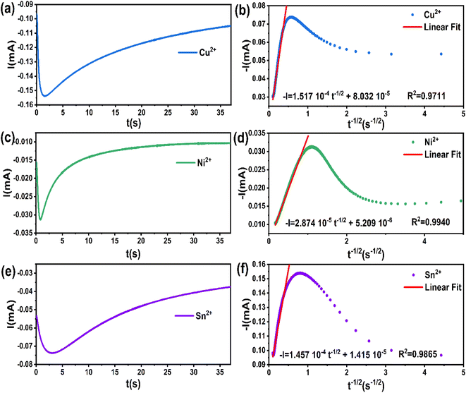 |
| | Fig. 5 Transients current and their plots according to the Cottrell equation for: (a and b) Cu2+, (c and d) Ni2+ and (e and f) Sn2+. The potentials applied are −0.62 V, −1.10 V and −1.05 V for Cu2+, Ni2+ and Sn2+ respectively. | |
 |
| | Fig. 6 (a) Schematic depiction of the nucleation and growth phenomena at various stages and (b) theoretical chronoamperometry plot for nucleation and growth mechanisms. | |
The chronoamperometry results obtained from the steady-state region of current versus time data (t ≥ tmax) can be utilized to calculate the diffusion coefficient for each element using Cottrell's equation (eqn (8)). In Fig. 5b, the data of the transients (t ≥ tmax) from Fig. 3a showed a satisfactory linear regression fit to the t−1/2 values.
| | |
I(t) = nFC(D/π)1/2t−1/2
| (8) |
where
I(
t) is the current,
nF is the molar number of electrons transferred during electrodeposition,
C is concentration,
D is the diffusion coefficient, and
t is the time.
Table 1 presented the diffusion coefficient values obtained for Cu
2+, Ni
2+ and Sn
2+. The low values of this parameter, in comparison with the literature,
30,31 are attributed to the complexation effect introduced by trisodium citrate at pH = 5.5.
Table 1 Calculated values of diffusion coefficient of Cu2+, Ni2+ and Sn2+
| Element |
Applied potential (V. vs. Ag/AgCl) |
Diffusion coefficient D (cm2 s−1) |
| Cu2+ |
−0.62 |
1.00 × 10⁻⁸ |
| Ni2+ |
−1.10 |
8.98 × 10⁻¹¹ |
| Sn2+ |
−1.05 |
1.64 × 10⁻⁸ |
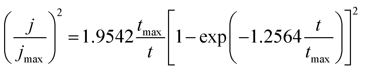
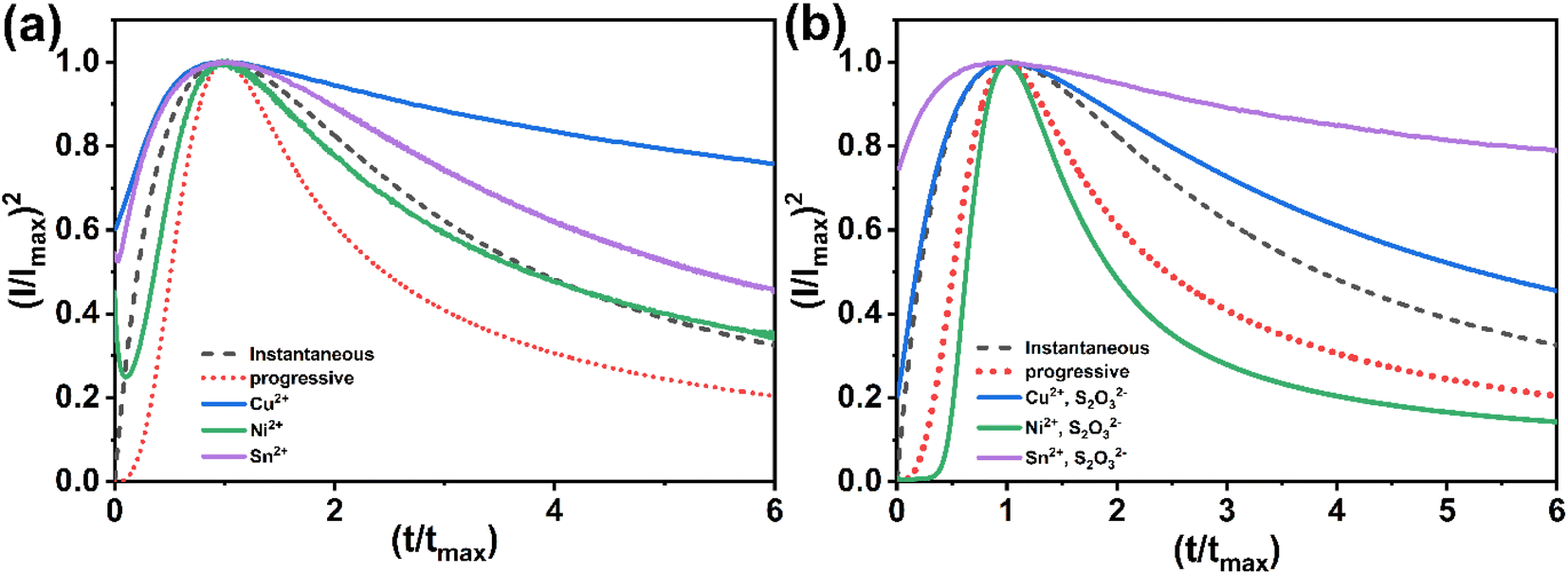
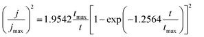
The non-dimensional curves proposed by Scharifker et al.,27,32 which depict the relationship between (I/Imax)2 and t/tmax, are commonly employed. According to this model, there exists two different modes of nucleation, namely instantaneous nucleation, and progressive nucleation. In the scenario where the rate of nucleation is considerably faster when compared to the resultant rate of growth, subsequent nuclei are formed at all potential growth sites within a very brief period, thus leading to the classification of nucleation as instantaneous. Conversely, if the rate of nucleation is slow, nucleation will persist to occur at the surface while the previous nucleation centers continue to grow, resulting in the term progressive nucleation. To investigate nucleation and the kinetics of growth, the experimental outcomes were compared to the theoretical model that was normalized in terms of the maximum current, Imax, as well as the time at which the current density reached its maximum value tmax. This is achieved by comparing experimental observations with theoretical predictions.27,33
For instantaneous nucleation:
| |
 | (9) |
And for progressive nucleation:
| |
 | (10) |
The current transients shown in Fig. 5a are plotted again in a dimensionless form in Fig. 7a and compared with the theoretical transients. The theoretical curves illustrating progressive nucleation and instantaneous nucleation (dotted lines) limited by diffusion growth are also presented. According to Fig. 7a it's shown that the curves of Cu2+ and Sn2+ are not described adequately by the theoretical models of instantaneous and nucleation growth. This behavior could be attributed to additional processes, such as the influence of a complexation agent or mass transport limitations.34 For Ni2+, the curve shows that probably the nucleation is both instantaneous and progressive before tmax and becomes instantaneous after tmax. In another hand, Fig. 7b presented the nucleation and growth mechanism of CNT precursor in presence of S2O32−. The curve for Sn2+ remains above the peak, while Cu2+ exhibits instantaneous nucleation before tmax and gradually conforms to the model after tmax. The Ni2+ curve demonstrates a transition to instantaneous nucleation after the addition of S2O32−. These behaviors can be explained by interactions between S2O32− and cations: it is possible to consider that the chemical reaction at the surface between the S2− ions generated in the bath and cations (eqn (1)–(5)) could alter the nucleation and growth mechanism process,21 additionally, the effect of complexation between metal ions and S2O32− may contribute to this behavior (eqn (11)).21,35 Fig. 3 demonstrates that S2O32− electrodeposition is induced by the presence of metallic ions, further impacting the nucleation and growth mechanism of the process.
| | |
2S2O32− + 2Cu2+ → S4O62− + 2Cu+
| (11) |
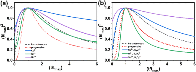 |
| | Fig. 7 Theoretical plots of instantaneous and progressive nucleation processes and experimental plots of: (a) CNT precursor, (b) CNT precursor in presence of S2O32−. | |
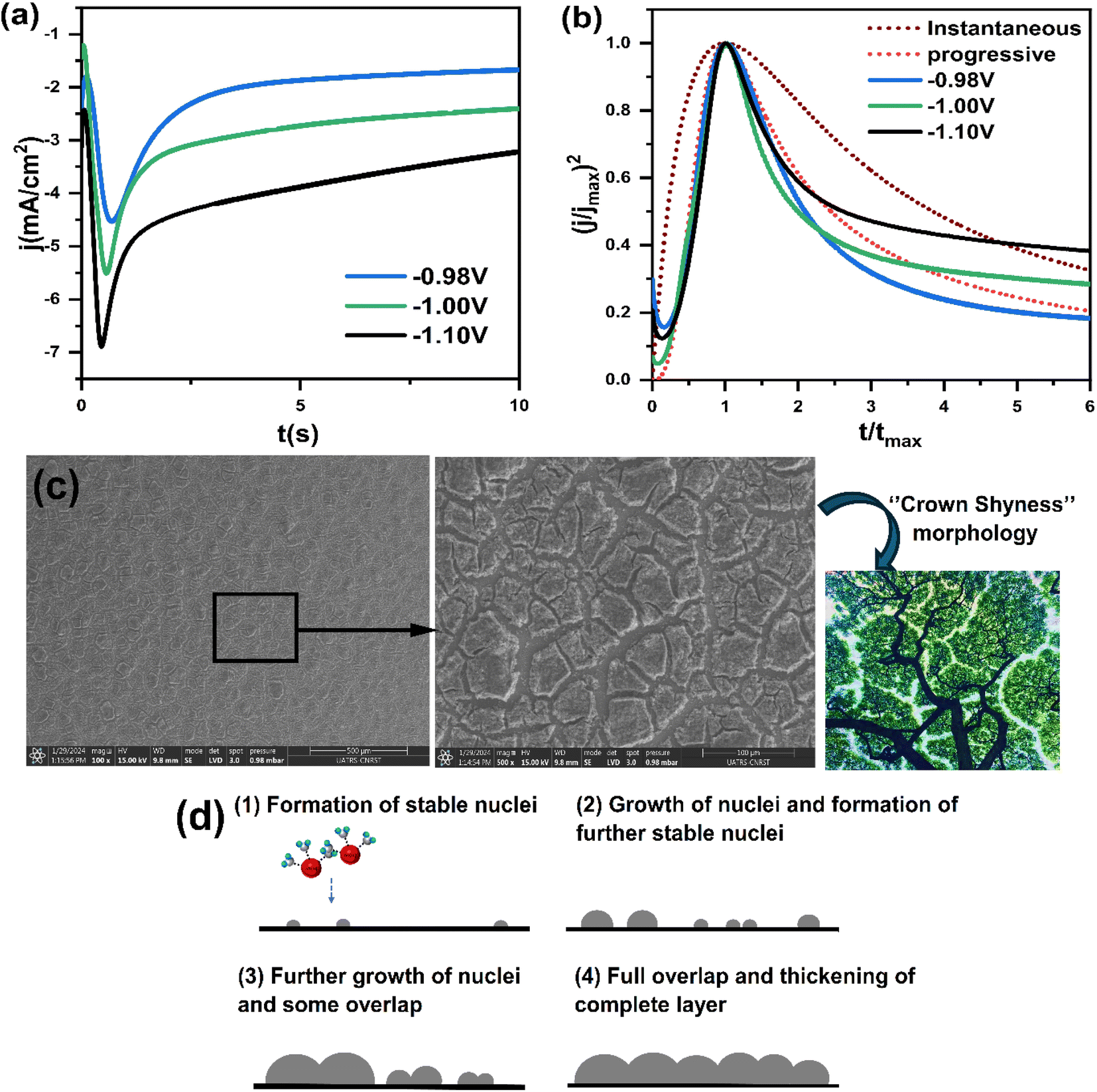
Fig. 8a presents a series of chronoamperometry curves for the CNTS precursor on the FTO electrode. Various potentials, namely −0.98 V, −1.00 V, and −1.10 V vs. g/AgCl, were applied. It was observed that the current intensity increased with higher applied potential. Furthermore, the transient current density profiles obtained in all cases reveal the nature of the electrochemical nucleation and growth process. Furthermore, Fig. 8a indicate that the transients exhibit a similar behavior, characterized by a rapid increase in current corresponding to the isolated growth of each individual nuclei and the increasing number of these nuclei present on the electrode surface, during which the transport of electroactive species to the nuclei formed on the surface occurs through hemispherical diffusion zones developed around each individual nucleus. As these nuclei grow, coalescence of adjacent diffusion zones with localized hemispherical nuclei results in a current maximum (Imax) followed by a decaying current, associated with diffusion-limited growth.30 These characteristics align with the nucleation of 3D hemispherical clusters followed by diffusion-limited growth.30 Fig. 8b illustrates the experimental data after normalization using the expressions (j/jmax)2 and (t/tmax). The corresponding theoretical model curves are also displayed. The observed representation indicates a significant agreement between the experimental plots and the progressive nucleation mode followed by 3D diffusion limited growth over the measured potential range. As a result, the rate of nucleation of CNTS precursor is slow, while the previous nucleation centers continue to grow.
 |
| | Fig. 8 (a) Transients current of CNTS precursor at different applied potentials, (b) the corresponding Scharifker–Hills' models, (c) SEM images of as deposited CNTS film deposited at −0.98 V, and (d) mechanism involving progressive nucleation and growth as hemispherical centers. | |
SEM examination of the surface of a CNTS (−0.90 V) thin film deposited on an FTO substrate revealed a dense film (Fig. 8c). Although the CFTS film covered the surface, it exhibited cracks. The morphology resembles a stone pattern or crown shyness in trees (Fig. 8c). As the deposition progresses, the size of CNTS nuclei increases, along with a rise in their quantity, suggesting a time-dependent progressive feature. This confirms the behavior mechanisms shown in Fig. 8b. In a progressive nucleation mechanism, an overpotential is required to drive the electron transfer reaction to form nuclei large enough to be stable. This process involves several distinct stages: nucleation of the new phase, growth of individual metal centers, overlapping of growing centers to form a complete layer, and thickening of the complete layer. These stages are shown in Fig. 8d.
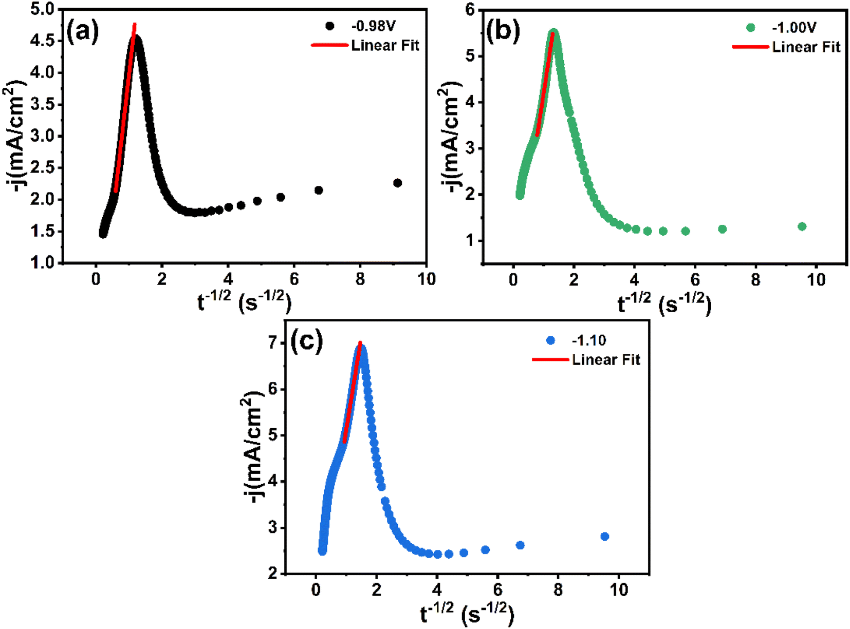
In Fig. 9, it is evident that the correlation between the values of j and t−1/2 during the final stages of the transient curves (t > tmax) exhibits linearity across the potential range. The above results confirm that the process of CNTS precursor deposition on an FTO substrate is limited by diffusion phenomena.
 |
| | Fig. 9 Transients current density (j) vs. (t−1/2) for the decreasing parts of Fig. 8a at different applied potentials: (a) −0.98 V, (b) −1.00 V and (c) −1.10 V. | |
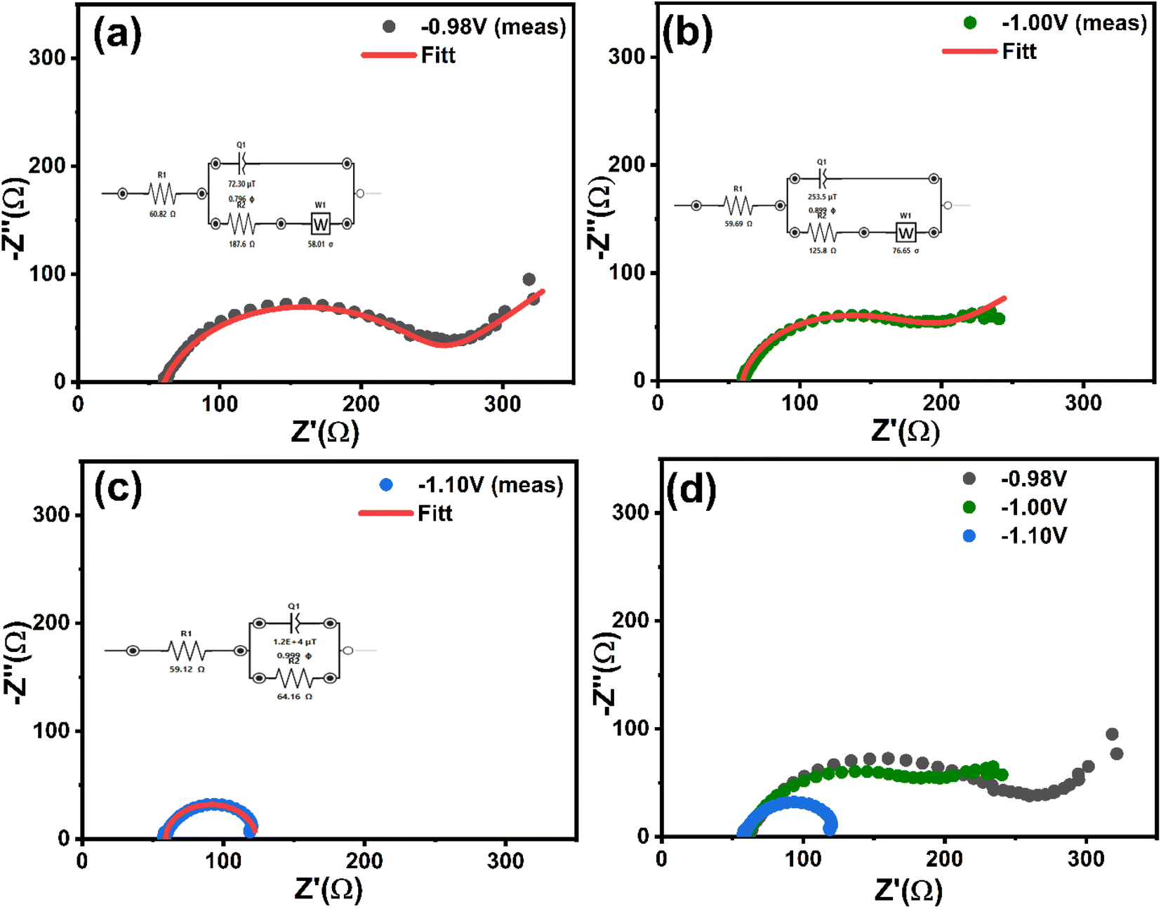
3.1.3 In situ electrochemical impedance spectroscopy (EIS). Fig. 10 presented an investigation of in situ electrochemical impedance spectroscopy (EIS) during electrodeposition of CNTS precursor at various applied potentials. Electrochemical transformations that occur at the electrode/electrolyte interface can be modeled by extracting components of the electronic equivalent circuits that correspond to the experimental impedance spectra. The circuit consists of several elements, namely the ohmic resistance of the electrolyte solution (Rs), the Warburg impedance (W), constant phase elements (CPEs) can be considered as non-ideal capacitors where the value of Q is analogous to that of capacitance, while also incorporating the factor of ideality, denoted by n, and the electron transfer resistance (Rct). Within the electronic circuit, the Rs and W components represent the overall characteristics of the electrolyte solution and the diffusion behavior of the redox elements in the solution, respectively.36 Fig. 11. Presents a schematic illustration of the succussive steps involved in electrodeposition and its equivalent circuits. As the charging of the electric double-layer capacitor progressed, the overpotential across the double layer became sufficient to initiate the ion discharge reaction. Concurrently, nucleation and growth took place, as depicted in the schematic illustration in Fig. 11a. The corresponding circuit model for this process consisted of two resistors and a capacitor in series (R(RQ)), as demonstrated in Fig. 11c. Throughout the nucleation and growth stages of the deposits, the diffusion zones surrounding the center do not bring enough ions for discharge, resulting in a slowdown of the electrodeposition rate controlled by diffusion control (Fig. 11b). The equivalent circuit included two resistors, a capacitor, and an inductance caused by diffusion denoted “W”, connected in series (R(Q(RW))), as shown in Fig. 11d. In the process, the diffusion region around each active point was expanded, resulting in an overlapping region, as shown in Fig. 11b.36
 |
| | Fig. 10 In situ EIS measurements during electrodeposition of CNTS precursor at different applied potentials: (a) −0.98 V, (b) −1.00 V, (c) −1.10 V, and (d) comparison of all EIS curves. | |
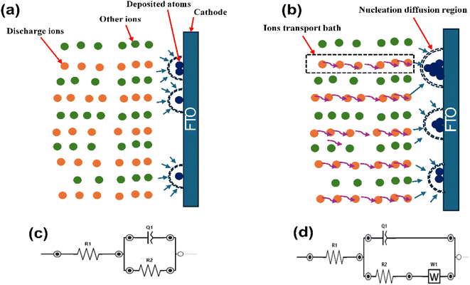 |
| | Fig. 11 Schematic depiction and corresponding circuitry during electrodeposition process. (a) Nucleation and growth; (b) diffusion control process and diffusion region overlap; (c) equivalent circuit for nucleation and growth; (d) equivalent circuit for diffusion control process. | |
The Nyquist plots, represented by the dotted curves in Fig. 10, extend a frequency range from 0.01 Hz to 100 kHz under an amplitude of 0.01 V. In all cases the EIS spectra depict capacitive behavior at high frequencies through semicircles, specifically related to interfacial impedance. This includes capacitance associated with double layer or electron transfer. Fig. 10a and b shows the appearance of Warburg impedance indicated by 45° straight line. This impedance arises from the transport of CNTS precursor in the solution and becomes more prominent at higher frequencies as the deposition potential becomes more negative. Moreover, the lack of Warburg impedance presented in Fig. 10c at applied potential of −1.10 V could suggest that the electrodeposited layer is comparatively thin. Within the Nyquist plots (Fig. 10d), the diameter of the semicircle reflects the Rct value, which indicates the redox conversion of the electroactive marker CNTS precursor on the electrode at a given potential. As we can see in Table 2, the electrochemical response decreases at −1.10 V (64.16 Ω) compared to the response at −1.00 V (125.80 Ω) and at −0.98 V (187.60), which indicate the rapid electron transfer process of CNTS precursor at −1.10 V.37
Table 2 Fitted parameter values obtained from EIS measurements at various applied potentials
| Applied potential (V. vs. Ag/AgCl) |
Rs (Ω) |
Rct (Ω) |
W (Ω s−0.5) |
CPE |
| Q (S sn) |
n (×10−3) |
| −0.98 |
60.82 ± 0.60 |
187.60 ± 1.19 |
58.01 ± 3.76 |
0.072 ± 0.005 |
796 ± 1.13 |
| −1.00 |
59.69 ± 2.60 |
125.80 ± 6.23 |
76.65 ± 7.66 |
0.253 ± 0.013 |
899 ± 4.58 |
| −1.10 |
59.12 ± 1.09 |
64.16 ± 4.62 |
— |
12.0 ± 0.25 |
999 ± 3.10 |
3.2. Structure and properties of the sulfurized thin films composed of CNTS
The precursor thin films were electrodeposited at 550 °C for 1 hour in the presence of sulfur powder.38 The structural and properties of the resulting CNTS thin films are presented in the following study.
3.2.1 XRD analysis. Fig. 12 presented the XRD patterns of CNTS films electrodeposited at different reduction potential. The characteristic peaks observed around 28.80°, 47.54°, and 56.73° correspond to the (111), (220), and (311) planes, respectively of the Cu2NiSnS4 cubic cell (space group F![[4 with combining macron]](https://www.rsc.org/images/entities/char_0034_0304.gif) 3m), as indicated in the powder diffraction file ICDD 00-026-0552 (ref. 39) (Fig. 12a), and are also consistent with previous findings studies.10,11,40 FTO reflection is presented at 38.04°.41 The crystallinity of CNTS phase improved as the potential applied decreased. In addition to these peaks, there were additional peaks indicating the presence of impurity phases such as binary compounds (NiS2, CuS, and SnS) and a ternary compound (Cu2SnS3). The existence of the NiS2 phase can be deduced by the diffraction lines at 2θ = 27.02°, 31.84°, and 35.76° (ICDD 01-078-4702). The SnS and CuS phases can be noticed around 2θ = 31° (ICDD 04-008-7739, ICDD 00-23-0959 respectively). The ternary Cu2SnS3 phase exhibits identical reflection peaks, as depicted in Fig. 12b (ICCD 00-026-0552).
3m), as indicated in the powder diffraction file ICDD 00-026-0552 (ref. 39) (Fig. 12a), and are also consistent with previous findings studies.10,11,40 FTO reflection is presented at 38.04°.41 The crystallinity of CNTS phase improved as the potential applied decreased. In addition to these peaks, there were additional peaks indicating the presence of impurity phases such as binary compounds (NiS2, CuS, and SnS) and a ternary compound (Cu2SnS3). The existence of the NiS2 phase can be deduced by the diffraction lines at 2θ = 27.02°, 31.84°, and 35.76° (ICDD 01-078-4702). The SnS and CuS phases can be noticed around 2θ = 31° (ICDD 04-008-7739, ICDD 00-23-0959 respectively). The ternary Cu2SnS3 phase exhibits identical reflection peaks, as depicted in Fig. 12b (ICCD 00-026-0552).
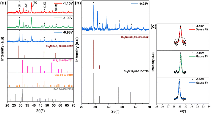 |
| | Fig. 12 (a) XRD patterns of CNTS sulfurized films at different applied potentials, (b) XRD patterns of CNTS film obtained at −0.98 V and (c) the mean peak intensity of 112 reflections. | |
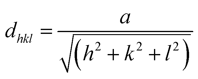
Structural parameters such as the lattice parameters (a, b, and c), the reticular distance (dhkl), the full width at half maximum (β), the average crystallite size (D), the microstrain (ε), and the dislocation density (δ) were determined. The values of the reticular distance for CNTS thin films on the mean peak (111) plane were calculated using the Bragg equation (eqn (12)).42
| |
nλ = 2dhkl![[thin space (1/6-em)]](https://www.rsc.org/images/entities/char_2009.gif) sinθ sinθ
| (12) |
As mentioned above, the CNTS thin films have a cubic structure, resulting in equal lattice parameters (a = b = c). Therefore, the lattice parameters were determined using the formula for reticular distance (eqn (13)). The Gaussian Fourier transform of the primary peak (111) is shown in Fig. 12c. The average crystallite size (D) is determined using the Debye–Scherrer formula (eqn (13)).
| |
 | (13) |
| |
 | (14) |
In this equation (
eqn (14)), the shape factor (
k = 0.9) is denoted by the variable
k, the X-ray wavelength (1.5406 Å) is represented by the symbol
λ, the full width at half maximum (FWHM) is denoted by
β, and the Bragg diffraction angle is represented by the symbol
θ.
The microstrain (ε) can be formulated as follows (eqn (15)):40
| |
 | (15) |
The dislocation density (δ) can be assessed using the Williamson and Smallman formula (eqn (16)):43
| |
 | (16) |
Details of comprehensive data, encompassing the primary structural parameters, are presented in Table 3.
Table 3 Structural parameters of CNTS electrodeposited thin films
| Applied potential (V) |
(hkl) |
2θ (°) |
β (°) |
D (nm) |
d-Spacing (Å) |
a = b = c (Å) |
ε |
δ (nm−2) |
| −0.98 |
111 |
28.897 |
0.004712 |
30.40 |
3.090 |
5.351 |
0.00457 |
0.00108 |
| −1.00 |
111 |
29.143 |
0.004398 |
32.60 |
3.064 |
5.307 |
0.00422 |
0.00094 |
| −1.10 |
111 |
28.995 |
0.006475 |
22.13 |
3.080 |
5.333 |
0.00626 |
0.00204 |
The crystallite size calculated using Debye–Scherrer formula was found to be 30.40 nm, 32.60 nm and 22.13 nm for CNTS these films electrodeposited at −0.98 V, −1.00 V and −1.10 V respectively. As can be seen, the crystallite size decreases at −1.10 V potential. In another hand, it is worth noting that the increase in grain size leads to a reduction in grain boundaries, which in turn reduces recombination and increases the effective diffusion length of minority carriers. This leads to an increase in short-circuit photocurrent in polycrystalline solar cells.44 The calculated value of the lattice parameter is a = 5.3 Å and other parameters are listed in Table 3.
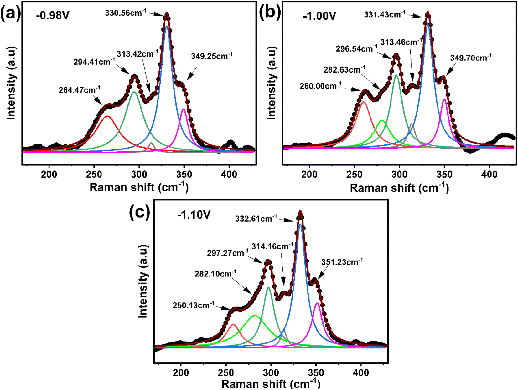
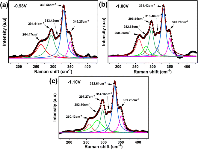
3.2.2 Raman analysis. Fig. 13 presents the Raman spectra analysis fitted using Lorentzian functions. The low peak intensity approximately at 282 cm−1 and the most intense peak around 330 cm−1 correspond to two peaks associated with the A1 vibration of the CNTS lattice.38,45 The peak at 282 cm−1 is not observed at −0.98 V. Conversely, based on the intensity and Full Width at Half Maximum (FWHM), the peak at 282 cm−1 shows a slight decrease in intensity as the deposition potential increases from −1.00 V to −1.10 V. Moreover, a higher intensity of the peak corresponds to larger crystallites and smaller micro-strain. These results agree with the XRD structural parameters given in Table 3. The peaks at 294–302 cm−1 and 345–350 cm−1 are characteristic of the orthorhombic CTS phase.46 The low-intensity peak observed between 312 and 317 cm−1 can be attributed to the surface-formed SnS2 and/or CTS,47 which increases as the potential rises. This phenomenon can be elucidated by the increased concentration of Sn element, as demonstrated by SEM mapping analysis shown in Fig. 14.
 |
| | Fig. 13 Raman spectra analysis of sulfurized CNTS thin films electrodeposited at different potentials: (a) −0.98 V, (b) −1.00 V and (c) −1.10 V. | |
 |
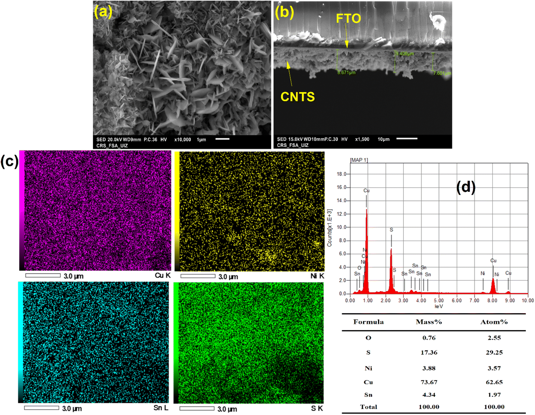
| | Fig. 14 (a) SEM image, (b) cross-sectional, (c) the individual elemental mappings and (d) the EDS analysis of the sulfurized CNTS thin film deposited at −0.98 V. vs. Ag/AgCl. | |
3.2.3 SEM-EDS-mapping. Fig. 14a shows the morphology of sulfurized CNTS thin films deposited at −0.98 V vs. Ag/AgCl on FTO-coated glass substrates.48–50 The SEM images of the surfaces of CNTS films at potentials of −0.98 depict a microsheets structure with a somewhat homogeneous surface and uniform size distribution. Moreover, the presence of numerous large voids and/or cavities is noticeable. The thickness of CNTS film was found to be homogeneous and measured around 8 μm (Fig. 14b).The SEM-EDX elemental mapping technique provides insight into the spatial distribution of various compositional elements. The same figure displays the elemental mapping for Cu, Ni, Sn and S of the CNTS thin films revealing approximately uniform distribution of all compositional elements (Fig. 14c). The concentration of Cu was found to be important, which may indicate the low complexation with tri-sodium citrate, while the Ni and Sn EDS analysis have the same concentration (Fig. 14d).
3.2.4 Optical analysis. The optical band gap energy of CNTS films, electrodeposited in various electrolytes, was determined using Tauc's relation (eqn (17)). This involved extending the linear portion of the graph that illustrates the relationship between (αhν)2 and energy (hν) through extrapolation.| | |
αhν = (A(hν − Eg))1/2
| (17) |
The optical characteristics of the synthesized CNTS nanocrystals are illustrated in Fig. 15a. A broad optical absorption in the visible range and a tail extending to longer wavelengths can be observed from the measurement. As is commonly understood, Cu2NiSnS4 is a direct bandgap semiconductor, with a bandgap value of approximately 1.5 eV. The optical band gap (Eg) of sulfurized CNTS samples electrode at different potential is determined by extrapolating the linear portion of the (αhν)2 versus photon energy (hν) curve to the intercept on the horizontal photon energy axis (Fig. 15b). The value of band gap is 1.68 eV, 1.73 eV and 1.89 eV for thin films CNTS −0.98 V, CNTS −1.00 V and CNTS −1.10 V respectively. The significant increase in band energy observed in CNTS −1.00 V and CNTS −1.10 V may be attributed to the presence of secondary phases.
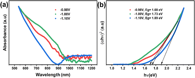 |
| | Fig. 15 (a) UV-visible absorption spectra and (b) band gap energy of CNTS thin films at different potential. | |
4. Conclusion
The CNTS thin films of absorbers made of low-cost, readily available, and environmentally safe have been synthesized through the process of electrodeposition with a constant applied potential followed by sulfurization at high temperatures. The electrochemical reduction behavior of Cu–Ni–Sn–S, as well as its nucleation and growth kinetics on the FTO-coated electrode surface, were investigated in trisodium citrate electrolyte solutions. We have demonstrated that the initial phase of CNTS precursor electrodeposition for all chosen potentials corresponds to three-dimensional progressive nucleation with growth controlled by diffusion of the nuclei. The nucleation mechanism is found to be influenced by the presence of S2O32− as well as inducing the electrodeposition of metal–S. In situ electrochemical impedance spectroscopy demonstrated capacitive behavior at high frequencies. However, the presence of Warburg diffusion was observed only for potentials lower than −1.0 V vs. Ag/AgCl. The cubic quaternary films with high crystallinity were achieved by applying −0.98 V vs. Ag/AgCl. SEM-EDS analysis revealed a uniform morphology of microsheets of sulfurized CNTS film, with a homogeneous thickness of 8 μm, while EDS indicated a significant concentration of Cu, suggesting low complexation by trisodium citrate. The optimal band gap energy, determined from the visible absorption spectra provided by CNTS electrodeposited at −0.98 V, was found to be −1.6 eV.
Data availability
Data will made available on request.
Conflicts of interest
The authors declare no competing interests.
Acknowledgements
We would like to express our gratitude to the Ministry of Higher Education, Scientific Research, and Professional Training (ENSSUP) CNRST for funding this work as part of the project in the priority areas of scientific research and development.
References
- O. Ait Layachi, S. Azmi, A. Moujib, M. Nohair and E. Khoumri, Investigation of nucleation and growth mechanism of Cu2ZnSnS4 absorber layer electrodeposition on Indium Tin Oxide coated glass, Thin Solid Films, 2023, 782, 140019, DOI:10.1016/j.tsf.2023.140019.
- A. Boudouma, O. Ait Layachi, H. Hrir and E. Khoumri, A one-step electrodeposition method was used to produce monoclinic Cu2SnS3 thin films for the development of solar cells, J. Mater. Sci.: Mater. Electron., 2023, 34, 1903, DOI:10.1007/s10854-023-11390-x.
- S. Azmi, A. Moujib, O. A. Layachi, E. Matei, A. C. Galca, M. Y. Zaki, M. Secu, M. I. Rusu, C. E. A. Grigorescu and E. M. Khoumri, Towards phase pure kesterite Cu2ZnSnS4 absorber layers growth via single step free sulfurization electrodeposition under a fix applied potential on Mo substrate, J. Alloys Compd., 2020, 842, 155821, DOI:10.1016/j.jallcom.2020.155821.
- H. Katagiri, N. Sasaguchi, S. Hando, S. Hoshino, J. Ohashi and T. Yokota, Preparation and evaluation of Cu2ZnSnS4 thin films by sulfurization of E-B evaporated precursors, Sol. Energy Mater. Sol. Cells, 1997, 49, 407–414, DOI:10.1016/S0927-0248(97)00119-0.
- H. Kirou, L. Atourki, L. Essaleh, A. Taleb, M. Y. Messous, K. Bouabid, M. Nya and A. Ihlal, Towards phase pure Kesterite Cu2ZnSnS4 thin films via Cu-Zn-Sn electrodeposition under a variable applied potential, J. Alloys Compd., 2019, 783, 524–532, DOI:10.1016/j.jallcom.2018.12.269.
- J. Zhou, X. Xu, H. Wu, J. Wang, L. Lou, K. Yin, Y. Gong, J. Shi, Y. Luo, D. Li, H. Xin and Q. Meng, Control of the phase evolution of kesterite by tuning of the selenium partial pressure for solar cells with 13.8% certified efficiency, Nat. Energy, 2023, 8, 526–535, DOI:10.1038/s41560-023-01251-6.
- C. Yan, C. Huang, J. Yang, F. Liu, J. Liu, Y. Lai, J. Li and Y. Liu, Synthesis and characterizations of quaternary Cu2FeSnS4 nanocrystals, Chem. Commun., 2012, 48, 2603, 10.1039/c2cc16972j.
- X. Zhang, N. Bao, B. Lin and A. Gupta, Colloidal synthesis of wurtzite Cu 2 CoSnS 4 nanocrystals and the photoresponse of spray-deposited thin films, Nanotechnology, 2013, 24, 105706, DOI:10.1088/0957-4484/24/10/105706.
- A. Kamble, K. Mokurala, A. Gupta, S. Mallick and P. Bhargava, Synthesis of Cu2NiSnS4 nanoparticles by hot injection method for photovoltaic applications, Mater. Lett., 2014, 137, 440–443, DOI:10.1016/j.matlet.2014.09.065.
- T.-X. Wang, Y.-G. Li, H.-R. Liu, H. Li and S.-X. Chen, Flower-like Cu2NiSnS4 nanoparticles synthesized by a facile solvothermal method, Mater. Lett., 2014, 124, 148–150, DOI:10.1016/j.matlet.2014.03.044.
- S. Sarkar, B. Das, P. R. Midya, G. C. Das and K. K. Chattopadhyay, Optical and thermoelectric properties of chalcogenide based Cu2NiSnS4 nanoparticles synthesized by a novel hydrothermal route, Mater. Lett., 2015, 152, 155–158, DOI:10.1016/j.matlet.2015.03.083.
- Y. Xie, C. Zhang, G. Yang, J. Yang, X. Zhou and J. Ma, Highly crystalline stannite-phase Cu2XSnS4 (X = Mn, Fe, Co, Ni, Zn and Cd) nanoflower counter electrodes for ZnO-based dye-sensitised solar cells, J. Alloys Compd., 2017, 696, 938–946, DOI:10.1016/j.jallcom.2016.12.043.
- D. Ait Elhaj, A. El Kissani, M. Elyaagoubi, H. Ait Dads, F. Welatta, L. Nkhaili, H. Chaib and A. Outzourhit, Development of Cu2NiSnS4 based thin film solar cells without a sulfurization step, Mater. Sci. Semicond. Process., 2020, 107, 104811, DOI:10.1016/j.mssp.2019.104811.
- N. Bitri, S. Dridi, F. Chaabouni and M. Abaab, Studies on the electrical properties of Cu2NiSnS4 thin films prepared by a simple chemical method, Mater. Lett., 2018, 213, 31–34, DOI:10.1016/j.matlet.2017.11.006.
- M. Beraich, M. Taibi, A. Guenbour, A. Zarrouk, A. Bellaouchou and M. Fahoume, Synthesis of Tetragonal Cu2NiSnS4 Thin Film via Low-Cost Electrodeposition Method: Effect of Ni2+ Molarity, J. Electron. Mater., 2020, 49, 728–735, DOI:10.1007/s11664-019-07707-4.
- S. Azmi, L. Pezzato, M. Sturaro, E. M. Khoumri, A. Martucci and M. Dabalà, A green and low-cost synthetic approach based on deep eutectic choline-urea solvent toward synthesis of CZTS thin films, Ionics, 2019, 25, 2755–2761, DOI:10.1007/s11581-018-2719-8.
- S. Azmi, E. M. Khoumri, L. Pezzato and M. Dabala, Influence of Solvent on the Proprieties of Cu2ZnSnS4 Thin Film Fabricated by One-Step Electrodeposition, Russ. J. Electrochem., 2019, 55, 796–801, DOI:10.1134/S1023193519070036.
- S. Azmi, L. Pezzato, M. Sturaro, E. M. Khoumri, A. Martucci and M. Dabalà, A green and low-cost synthetic approach based on deep eutectic choline-urea solvent toward synthesis of CZTS thin films, Ionics, 2019, 25, 2755–2761, DOI:10.1007/s11581-018-2719-8.
- V. A. Isaev, O. V. Grishenkova and Y. P. Zaykov, On the theory of 3D multiple nucleation with kinetic controlled growth, J. Electroanal. Chem., 2018, 818, 265–269, DOI:10.1016/j.jelechem.2018.04.051.
- V. A. Isaev, O. V. Grishenkova and Y. P. Zaykov, Theoretical modeling of electrochemical nucleation and growth of a single metal nanocluster on a nanoelectrode, RSC Adv., 2020, 10, 6979–6984, 10.1039/D0RA00608D.
- O. Ait Layachi, A. Moujib, O. El Khouja, A. Catalin Galca, A. Boudouma, S. Azmi, M. Nini, M. Nohair and E. Khoumri, Electrodeposition mechanism of Cu2CoSnS4 thin films onto FTO-coated glass: Effect of some additives, J. Electroanal. Chem., 2024, 959, 118177, DOI:10.1016/j.jelechem.2024.118177.
- A. V. Stanchik, T. N. Asmalouskaya, V. V. Rakitin, V. F. Gremenok, M. V. Gapanovich, E. L. Trukhanova, T. I. Zubar, A. V. Trukhanov and S. V. Trukhanov, Morphology and Crystal Structure of Cu2NiSn(S,Se)4 Thin Films Obtained by an Electrodeposition-Annealing Process, Coatings, 2022, 12, 1198, DOI:10.3390/coatings12081198.
- C. L. Yang, Y. H. Chen, M. Lin, S. L. Wu, L. Li, W. C. Liu, X. S. Wu and F. M. Zhang, Structural, optical and magnetic properties of Cu2NiSnS4 thin films deposited by facile one-step electrodeposition, Mater. Lett., 2016, 166, 101–104, DOI:10.1016/j.matlet.2015.12.054.
- H.-J. Chen, S.-W. Fu, T.-C. Tsai and C.-F. Shih, Quaternary Cu2NiSnS4 thin films as a solar material prepared through electrodeposition, Mater. Lett., 2016, 166, 215–218, DOI:10.1016/j.matlet.2015.12.082.
- K. Ç. Demir, The investigation of the corrosion behavior of CZTS thin films prepared via electrodeposition, Mater. Sci. Semicond. Process., 2021, 123, 105553, DOI:10.1016/j.mssp.2020.105553.
- F. Nasirpouri, Electrodeposition of Nanostructured Materials, Springer International Publishing, Cham, 2017, DOI:10.1007/978-3-319-44920-3.
- B. Scharifker and G. Hills, Theoretical and experimental studies of multiple nucleation, Electrochim. Acta, 1983, 28, 879–889, DOI:10.1016/0013-4686(83)85163-9.
- A. Mashreghi and H. Zare, Investigation of nucleation and growth mechanism during electrochemical deposition of nickel on fluorine doped tin oxide substrate, Curr. Appl. Phys., 2016, 16, 599–604, DOI:10.1016/j.cap.2016.03.008.
- S. Omanovic and M. Metikos-Hukovic, A study of the kinetics and mechanisms of electrocrystallization of indium oxide on an in situ prepared metallic indium electrode, Thin Solid Films, 2004, 458, 52–62, DOI:10.1016/j.tsf.2003.11.271.
- M. R. Khelladi, L. Mentar, A. Azizi, A. Sahari and A. Kahoul, Electrochemical nucleation and growth of copper deposition onto FTO and n-Si(100) electrodes, Mater. Chem. Phys., 2009, 115, 385–390, DOI:10.1016/j.matchemphys.2008.12.017.
- L. O. S. Bulhes and L. H. Mascaro, Electrochemical nucleation of lead and copper on indium-tin oxide electrodes, J. Solid State Electrochem., 2004, 8, 238–243, DOI:10.1007/s10008-003-0419-3.
- B. Scharifker and G. Hills, Electrochemical kinetics at microscopically small electrodes, J. Electroanal. Chem. Interfacial Electrochem., 1981, 130, 81–97, DOI:10.1016/S0022-0728(81)80378-6.
- S. Esmailzadeh, T. Shahrabi, Y. Yaghoubinezhad and Gh. B. Darband, An analytical study on nucleation and growth mechanism of nanostructured Ni-Se coating by the chronoamperometry and pulse potential techniques, J. Electroanal. Chem., 2021, 881, 114949, DOI:10.1016/j.jelechem.2020.114949.
- S. Azmi, M. Nohair, E. M. Khoumri, M. El Marrakchi and M. Dabala, Effect of the complexing agents on the properties of electrodeposited CZTS thin films, 7th International Conference on Renewable Energy Research and Applications, Paris, France, 2018, DOI:10.1109/ICRERA.2018.8566894.
- J. Wang, Md. M. Rahman, C. Ge and J.-J. Lee, Electrodeposition of Cu2S nanoparticles on fluorine-doped tin oxide for efficient counter electrode of quantum-dot-sensitized solar cells, J. Ind. Eng. Chem., 2018, 62, 185–191, DOI:10.1016/j.jiec.2017.12.056.
- O. Ait Layachi, Pulsed potential co-electrodeposition of Cu2CoSnS4 absorber layer on fluorinated tin oxide (FTO)-coated glass, J. Appl. Electrochem., 2024 DOI:10.1007/s10800-024-02131-x.
- X. Fan, Z. Li, S. Wang, L. Liu, P. Liu, F. Chen and X. Zheng, Electrochemical Impedance Biosensor for the Determination of Lipopolysaccharide Using Peptide as the Recognition Molecule, J. Braz. Chem. Soc., 2019, 30, 1762–1768, DOI:10.21577/0103-5053.20190081.
- O. El Khouja, K. Nouneh, M. Ebn Touhami, E. Matei, V. Stancu, M. Enculescu and A. C. Galca, Growth and characterization of Cu–Ni–Sn–S films electrodeposited at different applied potentials, J. Mater. Sci.: Mater. Electron., 2023, 34, 760, DOI:10.1007/s10854-023-10173-8.
- W. Schäfer and R. Nitsche, Tetrahedral quaternary chalcogenides of the type Cu2 II IV S4(Se4), Mater. Res. Bull., 1974, 9, 645–654, DOI:10.1016/0025-5408(74)90135-4.
- A. Jariwala, T. K. Chaudhuri, S. Patel, A. Toshniwal, V. Kheraj and A. Ray, Direct-coated copper nickel tin sulphide (Cu2NiSnS4) thin films from molecular ink, Mater. Lett., 2018, 215, 118–120, DOI:10.1016/j.matlet.2017.12.083.
- M. Oubakalla, M. Beraich, M. Taibi, H. Majdoubi, A. Guenbour, A. Bellaouchou, M. Addou, F. Bentiss, A. Zarrouk and M. Fahoume, Effects of copper concentration on the properties of Cu2CoSnS4 thin films co-electrodeposited on the FTO substrate, J. Mater. Sci.: Mater. Electron., 2022, 33, 12016–12025, DOI:10.1007/s10854-022-08162-4.
- M. El ouardi, A. Idrissi, H. Ahsaine, A. BaQais, M. Saadi and M. Arab, Current advances on nanostructured oxide photoelectrocatalysts for water splitting: A comprehensive review, Surf. Interfaces, 2024, 45, 103850, DOI:10.1016/j.surfin.2024.103850.
- G. K. Williamson and R. E. Smallman III, Dislocation densities in some annealed and cold-worked metals from measurements on the X-ray debye-scherrer spectrum, Philos. Mag., 1956, 1, 34–46, DOI:10.1080/14786435608238074.
- N. A. Bakr, S. A. Salman and S. A. Hameed, Deposition and Characterization of Cu2ZnSnS4 Thin Films for Solar Cell Applications, Int. J. Appl. Eng. Res., 2018, 13, 3379–3388 Search PubMed.
- P. Baskaran, K. D. Nisha, S. Harish, R. Ramesh, H. Ikeda, J. Archana and M. Navaneethan, Improved electrochemical performance of Cu2NiSnS4 hierarchical nanostructures as counter electrode in dye sensitized solar cells, Mater. Lett., 2022, 307, 130946, DOI:10.1016/j.matlet.2021.130946.
- I. S. Babichuk, M. O. Semenenko, S. Golovynskyi, R. Caballero, O. I. Datsenko, I. V. Babichuk, J. Li, G. Xu, R. Qiu, C. Huang, R. Hu, I. Golovynska, V. Ganus, B. Li, J. Qu and M. Leon, Control of secondary phases and disorder degree in Cu2ZnSnS4 films by sulfurization at varied subatmospheric pressures, Sol. Energy Mater. Sol. Cells, 2019, 200, 109915, DOI:10.1016/j.solmat.2019.109915.
- X. Zuo, K. Chang, J. Zhao, Z. Xie, H. Tang, B. Li and Z. Chang, Bubble-template-assisted synthesis of hollow fullerene-like MoS 2 nanocages as a lithium ion battery anode material, J. Mater. Chem. A, 2016, 4, 51–58, 10.1039/C5TA06869J.
- B.-E. Channab, A. El Idrissi, A. Ammar, A. Akil, J. C. White and M. Zahouily, ZIF-8 metal organic framework, carboxymethylcellulose and polyvinyl alcohol bio-nanocomposite controlled-release phosphorus fertilizer: Improved P management and tomato growth, Chem. Eng. J., 2024, 495, 153610, DOI:10.1016/j.cej.2024.153610.
- B.-E. Channab, A. El Idrissi, A. Ammar, O. Dardari, S. E. Marrane, A. El Gharrak, A. Akil, Y. Essemlali and M. Zahouily, Recent advances in nano-fertilizers: synthesis, crop yield impact, and economic analysis, Nanoscale, 2024, 16, 4484–4513, 10.1039/D3NR05012B.
- B. El Allaoui, H. Chakhtouna, N. Zari, H. Benzeid, A. el kacem Qaiss and R. Bouhfid, Process for cellulose-alginate core–shell microspheres fabrication and the influence of drying conditions on their structural and adsorption performances, Cellulose, 2024, 31, 5669–5686, DOI:10.1007/s10570-024-05954-1.
|
| This journal is © The Royal Society of Chemistry 2024 |
Click here to see how this site uses Cookies. View our privacy policy here. 
 Open Access Article
 This Open Access Article is licensed under a Creative Commons Attribution-Non Commercial 3.0 Unported Licence
 *a,
Hala Hrira,
Abderrazzak Boudoumaa,
Lahoucine Atourki
*a,
Hala Hrira,
Abderrazzak Boudoumaa,
Lahoucine Atourki