
 Open Access Article
 This Open Access Article is licensed under a Creative Commons Attribution-Non Commercial 3.0 Unported Licence
Synthesis of InAl-alloyed Ga2O3 nanowires for self-powered ultraviolet detectors by a CVD method†
Bei Liab,
Zhiyu Dongab,
Wei Xub,
Guowei Lib,
Xiaozhan Yang a,
Shuanglong Fenga,
Wenlin Feng*a and
Wenqiang Lu*b
a,
Shuanglong Fenga,
Wenlin Feng*a and
Wenqiang Lu*b
aSchool of Science, Chongqing University of Technology, Chongqing Key Laboratory of New Energy Storage Materials and Devices, Chongqing 400054, P. R. China. E-mail: fengwenlin@cqut.edu.cn
bChongqing Institute of Green and Intelligent Technology, Chinese Academy of Sciences, Multiscale Manufacturing Technology Lab, Chongqing School, University of Chinese Academy of Sciences, Chongqing, 400714, China. E-mail: wqlu@cigit.ac.cn
First published on 19th July 2024
Abstract
Ga2O3 is a kind of wide-band gap semiconductor, which has great potential in deep ultraviolet detection because of its high efficiency and fast response. Doping can improve the photoelectric properties of Ga2O3 materials. In this paper, In and Al elements alloyed Ga2O3 nanowires (InAl-Ga2O3 NWs) were successfully grown on p-GaN using a cost-effective chemical vapor deposition method and a vertical structure. The GaN/InAl-Ga2O3 NWs p–n self-powered wide-gap UV photodetector (PD) was constructed based on sputtered gold film as the bottom and top electrodes, and spin coated with polymethyl methacrylate as the insulating layer in the vertical direction. The GaN/InAl-Ga2O3 UV PD exhibits excellent performances, including an extremely low dark current of 0.015 nA, a maximum photocurrent of about 16 nA at zero-bias voltage under 265 nm illumination, and a light-to-dark current ratio greater than 103. The responsivity is 0.94 mA W−1, the specific detectivity is 9.63 × 10⁹ jones, and the good fast response/attenuation time is 31.2/69.6 ms. The self-powered characteristics are derived from the internal electric field formed between p-type GaN and n-type InAl-Ga2O3 NWs, which is conducive to the rapid separation and transfer of photogenerated carriers. This work provides an innovative mechanism of high-performance metal oxide nanowires for the application of p–n junction photodetectors, which can operate without any external bias.
1. Introduction
The ultraviolet (UV) spectrum of solar radiation is generally divided into the long-wave ultraviolet (UVA) spectrum (315–400 nm), the medium-wave ultraviolet (UVB) spectrum (280–315 nm), the short-wave ultraviolet (UVC) spectrum (100–280 nm), and the extreme ultraviolet (EUV) spectrum (10–121 nm).1–8 Ultraviolet radiation between 200 and 280 nanometers has a low background level at the Earth's surface because the Earth's ozone layer blocks 97–99% of the ultraviolet radiation that penetrates the atmosphere.9–17 Therefore, this region is called the solar blind region, and the solar blind ultraviolet photodetector has a high degree of selectivity for light radiation in the deep ultraviolet band (200–280 nm).18–21Ga2O3 has an ultra-wide band gap of 4.9 eV,22,23 and the orthogonal β-Ga2O3 structure is the most stable crystal phase of Ga2O3, which has the characteristics of large breakdown field, high electron mobility, excellent thermal stability and chemical stability.24–29 It has great potential in the fields of sun-blind UV photodetectors, photocatalysts, phosphors, gas sensors and light-emitting diodes. One-dimensional Ga2O3 nanowire (NW) photodetectors have a high body surface area ratio, which enhances their advantages in fast response and sensitivity.30–32 However, the high quality of nanomaterials and the stability of nanostructures are the existing problems. In order to improve the detection performance, people often regulated the optical and electrical characteristics of Ga2O3 by introducing doping elements and constructing heterojunctions.33–38 For example, Zhu et al.39 reported a Schottky junction UV photodetector spun with MXene on Ga2O3 nanowire, which is essentially MSM structured. Usman et al.40 reported a (In0.26Ga0.74)2O3 photodetector based on microwave irradiation assisted deposition technology, which is still a photoconductive device. Rahman et al.41 proved the practicability of doping compensation regulation in bandgap engineering. Most of the ultraviolet photodetectors based on Ga2O3 are two-dimensional thin film devices. At the same time, most of the ultraviolet photodetectors based on one-dimensional Ga2O3 nanowires p–n junction are realized by a die-casting method, or template method, which requires high equipment and complicated steps.
In view of these, in this work, we report a new sun-blind UV photodetector which is based on the GaN/InAl-Ga2O3 NWs p–n junction and has high performance and fast response. In this photodetector, In and Al alloyed Ga2O3 NWs were grown on GaN substrate by a simple and economical chemical vapor deposition (CVD) method, because CVD method which we used in this work can use raw materials more efficiently, reduce waste, and have a high material utilization rate comparing with methods such as physical vapor deposition (PVD), the melt drawing method and the laser ablation method requiring larger equipment. And also, the structure of CVD equipment is relatively simple, the maintenance cost is low, and it has high stability for long-term operation. The presence of oxygen vacancy makes Ga2O3 NWs appear as n-type, which is combined with p-GaN to form a p–n junction, and the device exhibits strong rectification characteristics. Polymethyl methacrylate (PMMA) coated in Ga2O3 NWs is used as the insulating layer, and nanoscale gold film is used as the transparent conductive layer. The lattice match between GaN and Ga2O3 is high, which is conducive to the formation of high quality heterojunction. PMMA is one of the best transparent polymer materials at present, with strong insulation, easy processing, and better stability in the ultraviolet environment. By sputtering nano-scale gold film on Ga2O3 NWs, the contact area between electrode and material can be increased and the electron flow efficiency can be enhanced. The results show that the GaN/InAl-Ga2O3 NWs p–n junction sun-blind UV photodetector has excellent comprehensive performances, and its dark current is extremely low, only 0.015 nA. At 265 nm illumination, the light–dark current ratio is greater than 103 under the condition of 0 bias voltage, the responsivity is 0.94 mA W−1. The specific detectivity is 9.63 × 10⁹ jones and the fast response/decay time is 31.2/69.6 ms. The internal mechanism of the self-powered photodetector is analyzed by means of energy band diagram. This work provides a simple and efficient strategy for the application of Ga2O3 nanowires in the field of self-powered UV photodetectors by improving both doping and heterojunction construction.
2. Experimental
2.1. Chemicals
GaSb (purity ≥99%), InSb (purity ≥99%) nano powder are purchased from Leyan, AlSb (purity ≥99% 200–300, mesh) powder is purchased from Beijing Jingmaiyan Material Technology Co., Ltd., the above source materials are not purified or treated. p-GaN is a sapphire epitaxial growth with a thickness of 4 μm, purchased from Puredo Optical Materials.2.2. Synthesis of InAl-Ga2O3 nanowires
GaN/InAl-Ga2O3 NWs was synthesized on p-GaN substrate by vapor deposition in a horizontal high temperature tube furnace. Firstly, 0.16 g of the powder mixture of InSb, GaSb and AlSb with a mass ratio of 1![[thin space (1/6-em)]](https://www.rsc.org/images/entities/char_2009.gif) :2:1 was put into the ceramic boat. A commercial p-type GaN epitaxial sheet (orientation: C-axis (0001) ± 0.5°; carrier concentration: 1017–1018 cm−3), with size 10 × 10 mm was used as substrate. After a standard cleaning of the substrate, a circular Au film with a thickness of approximately 5 nm and a diameter of 8 mm is sputtered in the middle area of the substrate with a sputtering coater and mask plate. Finally, at room temperature, the reactant and substrate are pushed into the middle of the quartz tube (quartz tube diameter 10 cm) in the tube furnace, the tube body is sealed, and the mechanical pump will be less than 1 pa. The heating program is set to be heated to 850 °C within 60 minutes. When the temperature is close to 500 °C, 100 sccm argon gas is used as the carrier gas, and the pressure in the tube is maintained at 200 Pa through the regulating valve. When the temperature is close to 850 °C, 1 sccm O2 is passed into the tube to participate in the reaction, and the reaction time is 3 min. After the reaction, immediately turn off O2 and Ar and cool the furnace to room temperature. Finally, a layer of gray material is obtained on the substrate surface as GaN/InAl-Ga2O3 NWs material.
:2:1 was put into the ceramic boat. A commercial p-type GaN epitaxial sheet (orientation: C-axis (0001) ± 0.5°; carrier concentration: 1017–1018 cm−3), with size 10 × 10 mm was used as substrate. After a standard cleaning of the substrate, a circular Au film with a thickness of approximately 5 nm and a diameter of 8 mm is sputtered in the middle area of the substrate with a sputtering coater and mask plate. Finally, at room temperature, the reactant and substrate are pushed into the middle of the quartz tube (quartz tube diameter 10 cm) in the tube furnace, the tube body is sealed, and the mechanical pump will be less than 1 pa. The heating program is set to be heated to 850 °C within 60 minutes. When the temperature is close to 500 °C, 100 sccm argon gas is used as the carrier gas, and the pressure in the tube is maintained at 200 Pa through the regulating valve. When the temperature is close to 850 °C, 1 sccm O2 is passed into the tube to participate in the reaction, and the reaction time is 3 min. After the reaction, immediately turn off O2 and Ar and cool the furnace to room temperature. Finally, a layer of gray material is obtained on the substrate surface as GaN/InAl-Ga2O3 NWs material.
2.3. Photodetector fabrication
An insulating layer was prepared on GaN substrate using spin coating and reactive ion etching (RIE) techniques. A 6% PMMA chlorobenzene solution was spun on the substrate at 4000 rpm for 40 seconds and dried at 100 °C for 10 minutes. PMMA covers the nanowires and fills the spaces between them. The PMMA-covered substrate is then etched 20 s with O2/Ar in RIE's reaction chamber, exposing part of the nanowires while remaining insulated. After the insulation layer is formed, Au film with a thickness of about 12 nm is plated on the surface of PMMA by magnetron sputtering. Finally, a physical mask was used to deposit a gold film of about 350 nm on GaN and PMMA as the bottom electrode and top electrode, respectively.2.4. Material and photoelectric characterization
All the as-grown nanowire networks were characterized by electron scanning electron microscopy (FE-SEM, JEOL7800F), energy dispersive X-ray spectrometer (EDS) (GENESIS 2000 XMS60S), high resolution transmission electron microscopy (HRTEM, JEM2100) operating at 200 kV, (JEOL), X-ray diffractometer (Rigaku RINT2500 TRAX-III, Cu Kα radiation) and UV-3101PC scanning spectrophotometer. The response calibration system (Zolix DSR600-3110-UV) was used to measure the spectral response of the detector. The current–voltage (I–V) characteristics and optical response of GaN/InAl-Ga2O3 NWs solar blind UV photoelectric detector were measured with a source meter (Keithley2450). UV lights with wavelengths of 255, 265 and 310 nm were used as the light sources, the intensities of all light sources were carefully calibrated using an optical power meter (OPHIR) before measurement. A beam shutter (GCI-73, GCI-7103M, Daheng New Era Technology) was used for time resolution measurement. Optical power density was measured using an optical power meter (S120VC, Thorlabs). All measurements were taken at room temperature.3. Result and discussion
The preparation process of GaN/InAl-Ga2O3 photodetector is shown in Fig. 1(a). InAl-Ga2O3 NWs was synthesized by chemical vapor deposition in a tube furnace (Fig. S1†). The GaN/InAl-Ga2O3 photodetector was prepared by using the etched PMMA as the insulating layer, then sputtering Au film as the transparent conductive layer (TCL), and finally the electrode was drawn to the printed circuit board (PCB) by bonding process. Fig. S2 and S3† are GaN/InAl-Ga2O3 p–n junction diagram and GaN/InAl-Ga2O3 photodetector diagram, respectively. In this process, the factors affecting the electrical conductivity of the device include two aspects: one is the number of exposed InAl-Ga2O3 NWs, that is to say, etching time (ET), the greater the ET, the more exposed InAl-Ga2O3 NWs; the other is the contact area between electrode and InAl-Ga2O3 NWs. We can increase the contact area between electrode and InAl-Ga2O3 NWs by sputtering a layer of Au film as TCL. First of all, the influence of ET on photocurrent is shown in Fig. S4(a).† Under the condition of no gold-plated film, ET ≤ 10 s will lead to open circuit, ET ≥ 20 s will lead to short circuit of the device, and the etching time of 20 s is the best time. Then, we explored the influence of TCL thickness on photocurrent (Fig. S4(b)†). As the thickness increased, the conductivity increased while the light transmittance decreased. Compared with Fig. S4(a),† the device after sputtering Au film has a higher photocurrent, which proves that sputtered TCL can effectively collect current. The results show that the peak value of photocurrent is obtained when the thickness of Au film reaches 12 nm. To sum up, in this experiment, the etching time of PMMA insulation layer was set to 20 s, and the thickness of Au film (TCL) was set to 12 nm.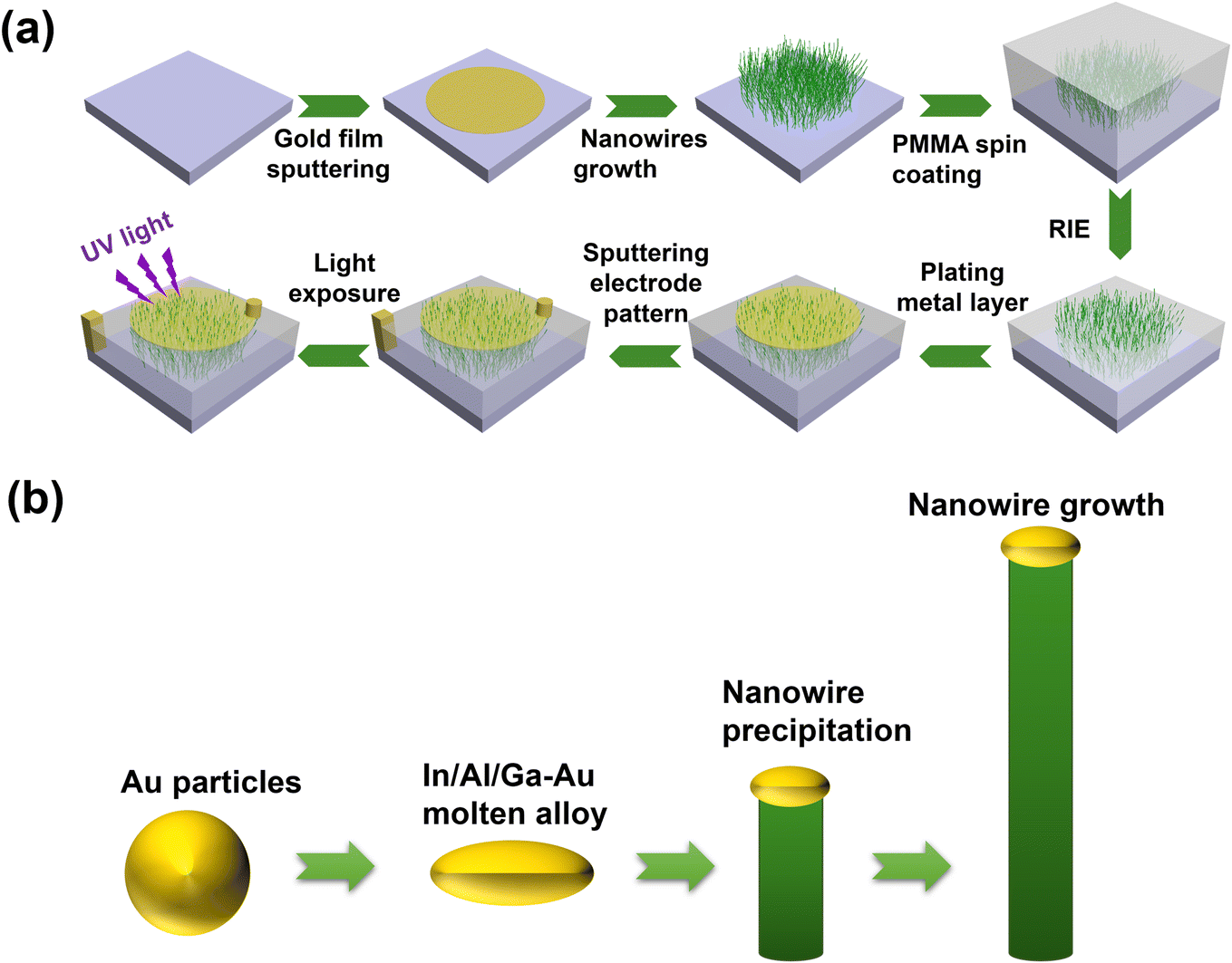 | ||
| Fig. 1 Process schematic diagram. (a) Preparation process flow chart. (b) Schematic diagram of InAl-Ga2O3 NWs growth principle. | ||
The growth principle of nanowires follows the vapor–liquid–solid (VLS) principle. In the VLS growth mechanism, the nanowires are grown layer by layer from the bottom up, and the resulting nanowires usually have excellent crystallinity and smoother crystal faces.22 As shown in Fig. 1(b), the mixture powders (InSb, GaSb and AlSb) are continuously heated to evaporate, and the antimony element in the antimonide material is easily vaporized and escapes at high temperature, resulting in Sb2O3 and corresponding metal cations. GaSb is first evaporated due to its low melting point and forms an AuGa2 molten alloy with molten gold particles, known as the “core” of the nanowires.42 As the temperature continues to rise, the “core” absorbs part of In3+ and Al3+. When the absorption is sufficient, a large amount of oxygen will be absorbed in the oxygen atmosphere to form an alloy and precipitate along a certain direction to form InAl-Ga2O3 NWs. In this process, the size of the “nucleus” can define the diameter of a particular nanowire.
High quality nanowires play a decisive role in the performance of devices. Fig. 2(a) shows the SEM top view of InAl-Ga2O3 NWs growing for 3 min under the set environmental conditions. The illustration shows the enlarged SEM top view. Fig. 2(b) shows the SEM cross-section of InAl-Ga2O3 NWs after growth for 3 min. InAl-Ga2O3 NWs has a diameter of about 60 nm and a length of about 3–5 μm. The bottom of the nanowires is relatively pure, most of the InAl-Ga2O3 nanowires grow vertically, and a few of them are offset and cross with other nanowires, thus forming a huge irregular nanowire network. The SEM cross-sections of InAl-Ga2O3 NWs growing for 3 min, 5 min and 10 min, respectively, are shown in Fig. S5.† With the continuous extension of growth time, the length of InAl-Ga2O3 NWs increases, while the bottom region of InAl-Ga2O3 NWs becomes more chaotic (Fig. S5(b)†). When the reaction time is 10 min (Fig. S5(c)†), InAl-Ga2O3 NWs are stacked together to form a “thin film” of InAl-Ga2O3 NWs, which is inconsistent with the one-dimensional material. Fig. 2(c) shows the EDS distribution diagram of InAl-Ga2O3 NWs after SiO2 growth for 3 min. In, Al, Ga and O elements are uniformly distributed in the material, and the corresponding atomic ratio is 0.86:1.39:3.08:4.67. Fig. 2(d) is the HRTEM diagram of a single nanowire of InAl-Ga2O3, showing a good single crystal degree. Fig. 2(d(i)) is the topography diagram, and Fig. 2(d(ii)) is the SAED pattern. It is calculated that the lattice spacing of this InAl-Ga2O3 is 0.472 nm, which is equal to the lattice spacing in the SAED pattern, and the corresponding crystal plane is the (−201) plane.
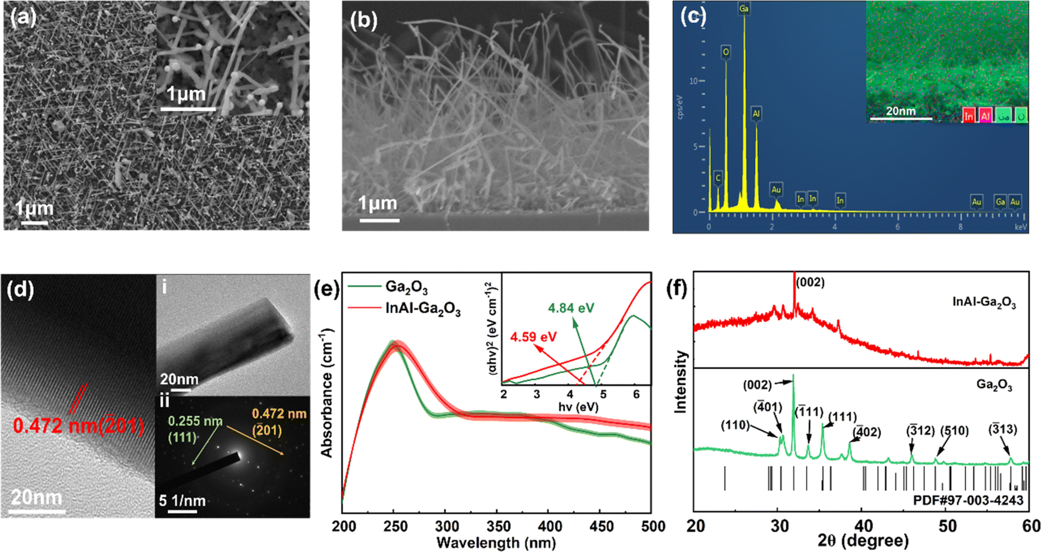 | ||
| Fig. 2 Characterization of material properties. (a) InAl-Ga2O3 NWs SEM top view and (b) sectional diagrams. (c) EDS spectra. The illustration is the distribution of elements. (d) InAl-Ga2O3 NWs TEM images, the inset HRTEM pictures and SAED patterns. (e) Ultraviolet absorption spectra of InAl-Ga2O3 NWs and Ga2O3 NWs deposited on Al2O3 substrate. The inset are Tauc plots according to Kubelka–Munk function of InAl-Ga2O3 NWs, Ga2O3 NWs. (f) XRD patterns of InAl-Ga2O3 NWs and Ga2O3 NWs. | ||
In order to further explore the influence of In and Al alloyed on Ga2O3, Fig. 2(e) and (f) show the ultraviolet absorption spectra and XRD patterns of InAl-Ga2O3 compared with Ga2O3. The ultraviolet absorption spectra show that both InAl-Ga2O3 and Ga2O3 have high absorption to the ultraviolet band, and have obvious absorption cutoff at about 300 nm, indicating that they have greater selectivity to the solar blind ultraviolet band. The band gap width of the semiconductor material is calculated by the following equation:39,43,44
| (αhυ)n = A(hυ − Eg)n | (1) |
Thus, it can be found from Fig. 2(e) that InAl-Ga2O3 has a band gap width of about 4.59 eV and has the highest radiation absorption at 265 nm, while Ga2O3 has a band gap width of about 4.84 eV and has the highest radiation absorption at 245 nm wavelength. The atomic size of In is larger than that of Ga, and its addition to Ga2O3 will cause the lattice constant of the material to increase. The atomic size of Al is smaller than that of Ga, and its addition to Ga2O3 will cause the lattice constant of the material to decrease. When In is added to Al-doped β-Ga2O3 (AGO), due to the compensation effect between the two dopants, as the concentration of In increases, when the doping ratio is 3.6 at%, the lattice constant of the material is greater than that of β-Ga2O3.45 The proportion of In in InAl-Ga2O3 is much greater than 3.6 at%, so the lattice constant of the material also increases, which is manifested as a red shift in the ultraviolet absorption spectrum. The diffraction peaks corresponding to InAl-Ga2O3 and Ga2O3 are highly matched with β-Ga2O3 (PDF#97-003-4243), with narrow diffraction peaks and no impurity diffraction peaks, indicating that InAl-Ga2O3 has only one phase and high crystal consistency, during the alloying process of In and Al elements, the β-Ga2O3 phase is retained without any additional intermediate phase.46
Fig. 3(a) is the structure diagram of the ultraviolet photodetector (UVPD) based on GaN/InAl-Ga2O3 NWs. Sputtered Au is used as the electrode, electrode 1 is the bottom electrode connected to the p-GaN substrate (and forms ohmic contact), and electrode 2 is the top electrode deposited on the surface of InAl-Ga2O3 NWs. Electrode 1 and electrode 2 are insulated. Fig. 3(b) shows the I–V characteristic curve of increasing current with increasing bias voltage in a dark environment, the dark current at 0 bias is 0.015 nA. The device shown in Fig. 3(b) has a strong single-pass characteristic attributed to the p–n junction of GaN/InAl-Ga2O3. In Fig. 3(c), we tested the UV spectral response of GaN/InAl-Ga2O3 NWs UVPD, and the results showed that the devices all responded in the UV region, were sensitive to 245 nm light, reached the maximum response at 265 nm light, and finally showed obvious cutoff response at 310 nm light. GaN bandgap is 3.4 eV, corresponding to wavelength up to 365 nm, which has an effect at 310 nm, so GaN/InAl-Ga2O3 NWs UVPD responds at 310 nm. This is in line with Fig. 2(e). Therefore, the following electrical performance tests use light at 245 nm, 265 nm, and 310 nm. GaN/InAl-Ga2O3 NWs UVPD can operate in the absence of external power supply due to the photogenic volt effect of p–n junction. Fig. 3(d) shows the I–V amplification curve of the GaN/InAl-Ga2O3 p–n junction near 0 bias. In the dark, the current is approaching zero at 0 V. Ultraviolet light irradiates the photodetector, producing unbalanced photogenerated charge carriers and forming an electric current. The transient photocurrents of 255 nm, 265 nm and 310 nm light sources with 150 μW cm−2 were 3.85 nA, 7.69 nA and 2.31 nA, respectively. It shows that the device has good self-power supply characteristics.
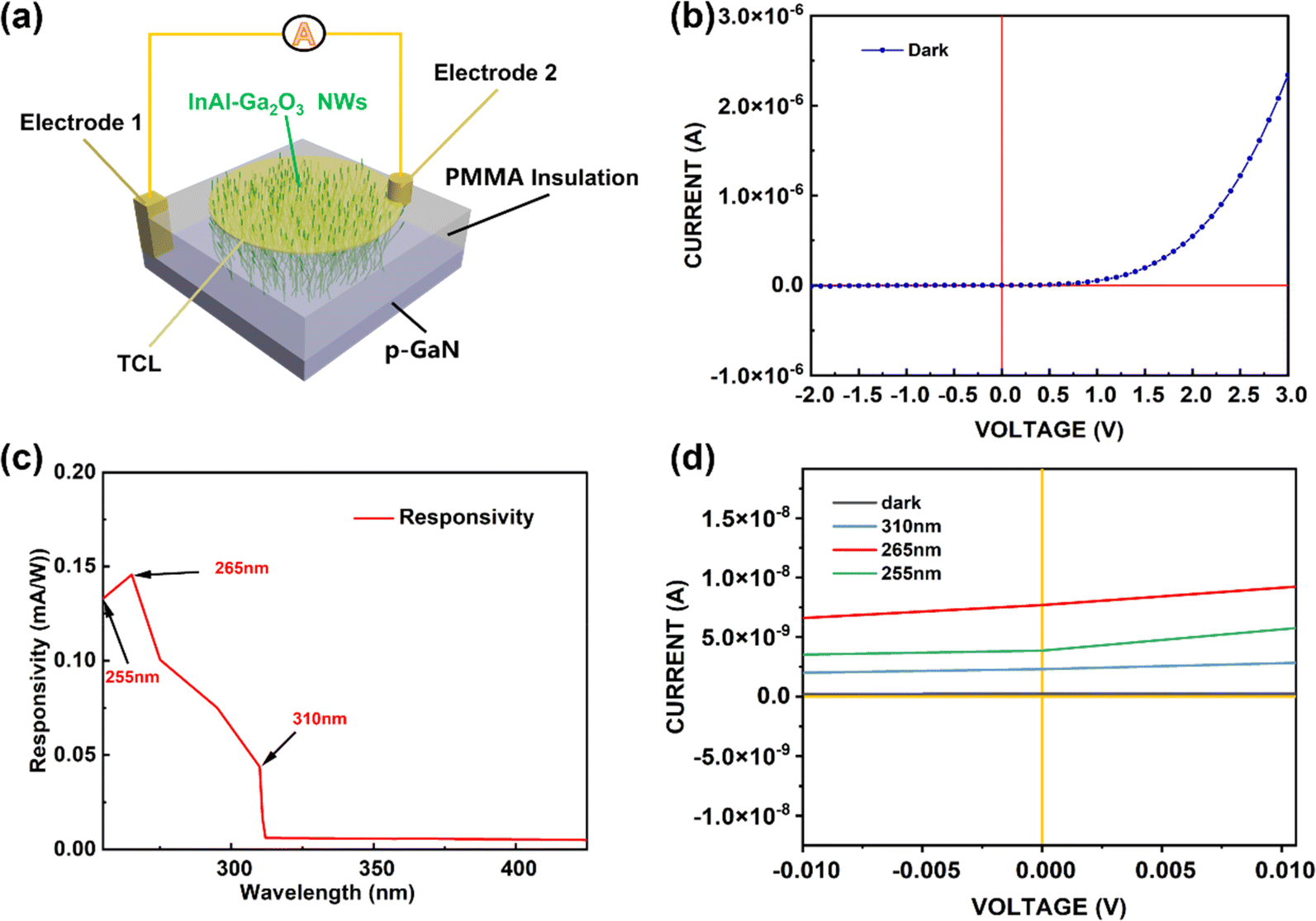 | ||
| Fig. 3 The structure and characteristics of GaN/InAl-Ga2O3 NWs UVPD. (a) Structure diagram of GaN/InAl-Ga2O3 NWs UVPD. (b) GaN/InAl-Ga2O3 NWs UVPD I–V characteristic curve. (c) Spectral response curve of GaN/InAl-Ga2O3 NWs UVPD. (d) I–V characteristic amplification curves of near zero bias for 255 nm, 265 nm and 310 nm light sources. | ||
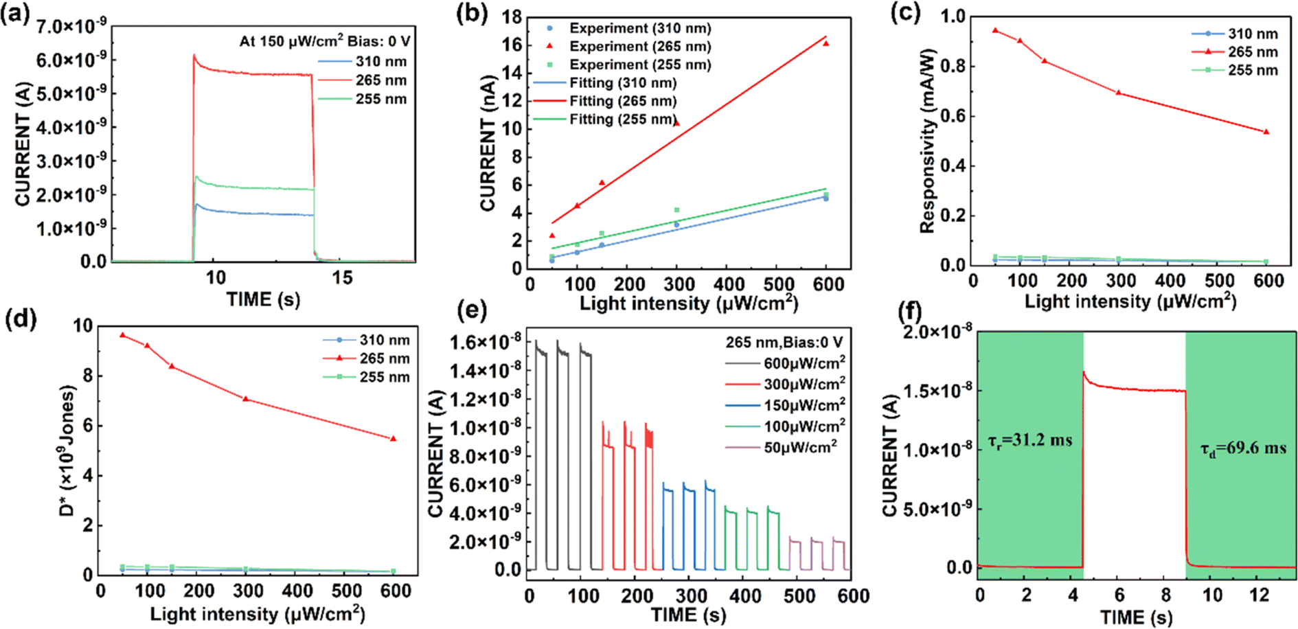
The dynamic responsivity of the device was also tested under zero-bias conditions by irradiating 255 nm, 265 nm and 310 nm light sources of 150 μW cm−2, as shown in Fig. 4(a). The photocurrents were 2.23 nA, 5.66 nA and 1.18 nA, respectively. Under the irradiation of 310 nm light source, the photocurrent drops sharply, indicating that the detector has a good cutoff response, and further highlighting the high selectivity of the device to 265 nm radiation. Fig. 4(b) shows the influences of 255 nm, 265 nm and 310 nm light sources with different optical power densities on the photocurrent of the device. With the increase of power, the gain of 265 nm light source on the photocurrent is the strongest.
 | ||
| Fig. 4 Electrical testing of GaN/InAl-Ga2O3 NWs UVPD: (a) light responses generated by different light sources under the same light intensity, GaN/InAl-Ga2O3 NWs UVPD at different light intensities of 255, 265 and 310 nm. (b) Photocurrent. (c) Responsivity. (d) Specific detectivity. (e) Dynamic optical response curve of GaN/InAl-Ga2O3 NWs UVPD under illumination of 265 nm light source with different powers. (f) Response and recovery speed of the device under 265 nm light source. | ||
In order to further clarify the optical response characteristics of the photodetector, the photoelectric conversion capability can be well described by calculating the optical responsivity:22,42
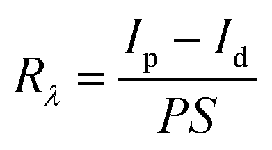 | (2) |
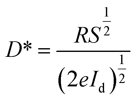 | (3) |
The dynamic responsivity of the device was also tested under zero-bias conditions by irradiating 255 nm, 265 nm and 310 nm light sources of 150 μW cm−2, as shown in Fig. 4(a). The photocurrents were 2.23 nA, 5.66 nA and 1.18 nA, respectively. Under the irradiation of 310 nm light source, the photocurrent drops sharply, indicating that the detector has a good cutoff response, and further highlighting the high selectivity of the device to 265 nm radiation. Fig. 4(b) shows the influences of 255 nm, 265 nm and 310 nm light sources with different optical power densities on the photocurrent of the device. With the increase of power, the gain of 265 nm light source on the photocurrent is the strongest.
Fig. 4(c) and (d) respectively show the responsivity and detectability of the device under the irradiations of 255 nm, 265 nm and 310 nm light sources at different optical power densities. The above results prove that GaN/InAl-Ga2O3 NWs UVPD has excellent performance under 265 nm radiation. Subsequently, 265 nm light is irradiated to GaN/InAl-Ga2O3NWs UVPD, and the light source is turned on/off every 20 s at different optical power densities and current data is collected in real time to draw Fig. 4(e). As shown in Fig. 4(e), the photocurrent intensity depends on the change of optical power density, and the dynamic photoresponse of GaN/InAl-Ga2O3 NWs UVPD under different conditions has high stability and periodicity.
In order to evaluate the response speed of GaN/InAl-Ga2O3 NWs UVPD under 265 nm illumination, the exponential relaxation equation is used to fit the transient optical response:52,53
| I = I0 + Ae−t/τ1 + Be−t/τ2 | (4) |
PDCR is the ratio of the device current between the light source on state and the light source off state, that is, the ratio of the photogenerated current to the dark current. In circuit design, PCDR is a very important parameter, which directly affects the performance and stability of the circuit, defined as:54
| PCDR = Ip/Id | (5) |
In order to further explain the self-powered working mechanism of p–n junction detector devices, the energy band diagram of GaN/InAl-Ga2O3 NWs UVPD is analyzed. The calculated bandgaps of InAl-Ga2O3 is 4.59 eV, and the bandgaps of GaN is 3.4 eV,22 respectively. Fig. 5(a) is the schematic diagram of the cross section structure of the device. As shown in the Fig. 5(a), ultraviolet light has good permeability in both TCL and PMMA, and the large number of gaps constructed in the InAl-Ga2O3 NWs greatly enhance the absorption and internal emission of incident light, thus enabling InAl-Ga2O3 NWs to have a higher absorption rate of ultraviolet light. Fig. 5(b) shows the band arrangements of InAl-Ga2O3 and GaN before contact. When n-type InAl-Ga2O3 NWs is grown on p-type GaN thin film substrate, due to the diffusion and recombination of most charge carriers (free electrons and holes), a space charge region is generated near the junction interface to form an internal electric field. The direction of the electric field is from n to p, forming a p–n junction. In the absence of an external power supply, the p–n junction finally reaches thermal equilibrium. Fig. 5(c) shows the band configuration of p–n junction formed by GaN/InAl-Ga2O3 under dark environment. When the p–n junction reaches thermal equilibrium, there is only a small amount of free electrons and hole migration in the interface. Fig. 5(d) shows the energy band configuration of p–n junction formed by GaN/InAl-Ga2O3 irradiated by ultraviolet light in a light environment. Ultraviolet light will excite a large number of electron–hole pairs and quickly break the thermal equilibrium state in GaN/InAl-Ga2O3 NWs UVPD. Under the action of the space charge region, the electron–hole pair separates rapidly. Electrons and holes are transferred to n-type InAl-Ga2O3 NWs and p-type GaN films respectively, and the thermal equilibrium state is also finally reached. By connecting the positive and negative electrodes of the device, a complete circuit is finally realized. The measurement results show that the current generated by GaN/InAl-Ga2O3 NWs UVPD under light is much larger than that under dark condition, and the device realizes self-powered UV light detection.
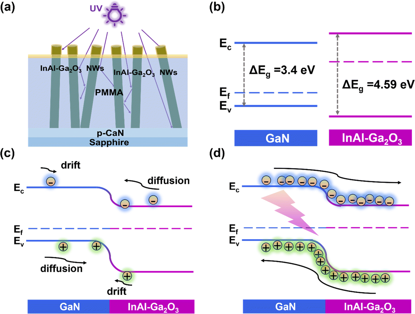 | ||
| Fig. 5 Band configuration analysis. (a) Schematic diagram of device cross-section structure. (b) GaN and InAl-Ga2O3 NWs band alignment before contact. Post-contact: (c) GaN/InAl-Ga2O3 p–n junction band arrangement in dark environment; (d) band map under zero-bias under UV irradiation. | ||
To illustrate the advantages of GaN/InAl-Ga2O3 NWs UVPD, Table 1 compares this work with work that have already been reported. The In and Al alloyed Ga2O3 nanowire photodetector has an R of about 90 times higher than that of the undoped Au/Ga2O3 detector and a D* of about 25 times higher than that of the Ga2O3/n-Si structure detector. The detector performance cannot be accurately compared under the influence of different test environments and test instruments, but it can be clearly seen from Table 1 that the parameters such as responsivity, specific detectivity and rise/fall time estimated in this study are comparable to or better than the reported values in the literature. The detector has excellent light-to-dark current ratio and specific detection capability at low power consumption. In addition, the fast response speed of the device is widely required in practical applications.
| Structure | Light condition | PDCR | R (mA W−1) | D* (jones) | Rise/decay time (ms) | Ref. |
|---|---|---|---|---|---|---|
| GaN/InAl-Ga2O3 NWs | 265 nm | 103 | 0.94 | 9.6 × 10⁹ | 31.2/69.6 | This work |
| Spiro-MeOTAD/Ga2O3/n-Si | 254 nm | 15 | 4.43 | 1.9 × 10⁷ | 30/196 | 55 |
| Ga2O3/n-Si | 254 nm | ∼600 | 0.22 | 4 × 10⁸ | 520/1620 | 55 |
| GaN/Ga2O3 | 254 nm | 80 | 28.44 | 6.2 × 10¹¹ | 140/70 | 56 |
| Ga2O3/Ga:ZnO |
254 nm | 127 | 0.76 | — | 179/272 | |
| NiO/Ga2O3 | 254 nm | 122 | 0.057 | 5.45 × 10⁹ | 340/3650 | 57 |
| CuI/a-IGZO | 356 nm | — | 0.6 | — | 22.5/95 | 58 |
| p-Graphene/γ-Ga2O3/nSiC | 250 nm | 152 | 5.8 | 7.6 × 10¹⁰ | 108/380 | 59 |
| NiO/IGZO heterojunction | 365 nm | — | 28.8 | 6.99 × 10¹⁰ | 15/31 | 60 |
| Au/Ga2O3 | 258 nm | ∼103 | 0.01 | — | 10−3/6 × 10−3 | 61 |
4. Conclusion
The vertical structure of GaN/InAl-Ga2O3 NWs photodetector is constructed by growing InAl-Ga2O3 nanowires on p-GaN by CVD method. Ga2O3 nanowires alloyed with In and Al elements have high crystallinity and high stability. The GaN/InAl-Ga2O3 UV PD exhibits excellent performance, including an extremely low dark current of 0.015 nA, a maximum photocurrent of about 16 nA under 265 nm 0 V illumination, and a light-to-dark current ratio greater than 103. The responsivity is 0.94 mA W−1, the specific detectivity is 9.63 × 10⁹ jones and the good fast response/decay time is 31.2/69.6 ms. In summary, the InAl-Ga2O3 nanowires optimize the crystal structure and enhance the material's capture of ultraviolet light, which is a promising deep ultraviolet photodetector. The material preparation process and device structure in this study can be applied to other photodetectors.Data availability
The data are stored in our research team's internal server, and access rights are limited to members of this research team. The datasets of the research results are available from the corresponding author upon reasonable request, and other supporting data are included in the ESI file.†Author contributions
Bei Li: conceptualization, methodology, software, investigation, formal analysis, writing – original draft. Zhiyu Dong: investigation. Wei Xu: visualization. Guowei Li: methodology. Xiaozhan Yang: supervision. Shuanglong Feng: supervision. Wenlin Feng: writing – review & editing, supervision, resources. Wenqiang Lu: writing – review & editing, supervision, resources.Conflicts of interest
The authors declare that they have no known competing financial interests or personal relationships that could have appeared to influence the work reported in this paper.Acknowledgements
The authors would like to acknowledge support from the National Natural Science Foundation of China (51574054), Natural Science Foundation of Chongqing, China (CSTB2024NSCQ-LZX0022), Chongqing Youth Science and Technology Talent Training Project (No. CQYC20210301363).Chongqing Municipal Education Commission (KJZD-K202201107), Chongqing Science and Technology Bureau (CSTC2021jcyj-msxmX0493, CSTB2022NSCQ-MSX0356), Joint Fund of Chongqing Municipal Education Commission and Science and Technology Bureau (CSTB2022NSCQ-LZX0032), Funding results of the Action Plan for the High-quality Development of Postgraduate Education of Chongqing University of Technology (No. GZLCX2022327).References
- X. H. Hou, Y. N. Zou, M. F. Ding, Y. Qin, Z. F. Zhang, X. L. Ma, P. J. Tan, S. J. Yu, X. Z. Zhou, X. L. Zhao, G. W. Xu, H. D. Sun and S. B. Lon, Review of polymorphous Ga2O3 materials and their solar-blind photodetector applications, J. Phys. D: Appl. Phys., 2021, 54(4), 34, DOI:10.1088/1361-6463/abbb45.
- P. Chinnamuthu and P. Pooja, Metal oxide heterostructures for light detector applications, in Metal Oxide-Based Heterostructures, ed. N. Kumar, B. M. Soucase and G. Korotcenkov, Elsevier, 2023, pp. 453–499 Search PubMed.
- D. Kaur and M. Kumar, A strategic review on gallium oxide based deep-ultraviolet photodetectors: recent progress and future prospects, Adv. Opt. Mater., 2021, 9(9), 34, DOI:10.1002/adom.202002160.
- T. He, X. D. Zhang, X. Y. Ding, C. Sun, Y. K. Zhao, Q. Yu, J. Q. Ning, R. X. Wang, G. H. Yu, S. L. Lu, K. Zhang, X. P. Zhang and B. S. Zhang, Broadband ultraviolet photodetector based on vertical Ga2O3/GaN nanowire array with high responsivity, Adv. Opt. Mater., 2019, 7(7), 7, DOI:10.1002/adom.201801563.
- X. Zhao, M. Ding, H. Sun and S. Long, Chapter five – controlling different phases of gallium oxide for solar-blind photodetector application, in Semiconductors and Semimetals, ed. Y. Zhao and Z. Mi, Elsevier, 2021, vol. 107, pp. 101–151 Search PubMed.
- S. J. Pearton, J. C. Yang, P. H. Cary, F. Ren, J. Kim, M. J. Tadjer and M. A. Mastro, A review of Ga2O3 materials, processing, and devices, Appl. Phys. Rev., 2018, 5(1), 56, DOI:10.1063/1.5006941.
- Y. T. Wu, X. Fu, K. Zhang, Z. Y. Tao, Y. X. Fan and W. Q. Lu, A strategy of high-sensitivity solar-blind photodetector for fabricating graphene surface modification ZnGa2O4/Ga2O3 core–shell structure nanowire networks, Ceram. Int., 2023, 49(11), 18248–18254, DOI:10.1016/j.ceramint.2023.02.196.
- Y. T. Wu, K. Zhang, G. W. Li, Q. S. Wang, X. Fu, L. Wang, J. L. Luo, S. L. Feng, Z. Y. Tao, Y. X. Fan and W. Q. Lu, Ultrafast response solar-blind UV sensor based on ZnGa2O4 nanowire bridge arrays, Phys. E, 2023, 146, 7, DOI:10.1016/j.physe.2022.115505.
- M. Higashiwaki, K. Sasaki, A. Kuramata, T. Masui and S. Yamakoshi, Gallium oxide (Ga2O3) metal-semiconductor field-effect transistors on single-crystal β-Ga2O3(010) substrates, Appl. Phys. Lett., 2012, 100(1), 3, DOI:10.1063/1.3674287.
- C. Wu, F. Wu, C. Ma, S. Li, A. Liu, X. Yang, Y. Chen, J. Wang and D. Guo, A general strategy to ultrasensitive Ga2O3 based self-powered solar- blind photodetectors, Mater. Today Phys., 2022, 23, 7, DOI:10.1016/j.mtphys.2022.100643.
- W. H. Ding and X. Q. Meng, High performance solar-blind UV detector based on β-Ga2O3/GaN nanowires heterojunction, J. Alloys Compd., 2021, 866, 7, DOI:10.1016/j.jallcom.2020.157564.
- C. Zhang, K. W. Liu, Q. Ai, X. Sun, X. Chen, J. L. Yang, Y. X. Zhu, Z. Cheng, B. H. Li, L. Liu and D. Z. Shen, High-performance fully transparent Ga2O3 solar-blind UV photodetector with the embedded indium-tin-oxide electrodes, Mater. Today Phys., 2023, 33, 6, DOI:10.1016/j.mtphys.2023.101034.
- Y. Qin, L. H. Li, X. L. Zhao, G. S. Tompa, H. Dong, G. Z. Jian, Q. M. He, P. J. Tan, X. H. Hou, Z. F. Zhang, S. J. Yu, H. D. Sun, G. W. Xu, X. S. Miao, K. H. Xue, S. B. Long and M. Liu, Metal-semiconductor-metal ε-Ga2O3 solar-blind photodetectors with a record-high responsivity rejection ratio and their gain mechanism, ACS Photonics, 2020, 7(3), 812–820, DOI:10.1021/acsphotonics.9b01727.
- D. Guo, Q. Guo, Z. Chen, Z. Wu, P. Li and W. Tang, Review of Ga2O3-based optoelectronic devices, Mater. Today Phys., 2019, 11, 19, DOI:10.1016/j.mtphys.2019.100157.
- H. L. Wang, L. S. Zhang, Z. G. Chen, J. Q. Hu, S. J. Li, Z. H. Wang, J. S. Liu and X. C. Wang, Semiconductor heterojunction photocatalysts: design, construction, and photocatalytic performances, Chem. Soc. Rev., 2014, 43(15), 5234–5244, 10.1039/c4cs00126e.
- J. C. Zhang, P. F. Dong, K. Dang, Y. N. Zhang, Q. L. Yan, H. Xiang, J. Su, Z. H. Liu, M. W. Si, J. C. Gao, M. F. Kong, H. Zhou and Y. Hao, Ultra-wide bandgap semiconductor Ga2O3 power diodes, Nat. Commun., 2022, 13(1), 8, DOI:10.1038/s41467-022-31664-y.
- K. Arora, N. Goel, M. Kumar and M. Kumar, Ultrahigh performance of self-powered β-Ga2O3 thin film solar-blind photodetector grown on cost-effective Si substrate using high-temperature seed layer, ACS Photonics, 2018, 5(6), 2391–2401, DOI:10.1021/acsphotonics.8b00174.
- H. B. Wang, H. Y. Chen, L. Li, Y. F. Wang, L. X. Su, W. P. Bian, B. S. Li and X. S. Fang, High responsivity and high rejection ratio of self-powered solar-blind ultraviolet photodetector based on PEDOT:PSS/β-Ga2O3 organic/inorganic p–n junction, J. Phys. Chem. Lett., 2019, 10(21), 6850–6856, DOI:10.1021/acs.jpclett.9b02793.
- T. Y. Zhai, L. Li, Y. Ma, M. Y. Liao, X. Wang, X. S. Fang, J. N. Yao, Y. Bando and D. Golberg, One-dimensional inorganic nanostructures: synthesis, field-emission and photodetection, Chem. Soc. Rev., 2011, 40(5), 2986–3004, 10.1039/c0cs00126k.
- B. Zhao, F. Wang, H. Y. Chen, Y. P. Wang, M. M. Jiang, X. S. Fang and D. X. Zhao, Solar-blind avalanche photodetector based on single ZnO-Ga2O3 core-shell microwire, Nano Lett., 2015, 15(6), 3988–3993, DOI:10.1021/acs.nanolett.5b00906.
- B. Zhao, F. Wang, H. Y. Chen, L. X. Zheng, L. X. Su, D. X. Zhao and X. S. Fang, An ultrahigh responsivity (9.7 mA W−1) self-powered solar-blind photodetector based on individual ZnO–Ga2O3 heterostructures, Adv. Funct. Mater., 2017, 27(17), 8, DOI:10.1002/adfm.201700264.
- G. W. Li, K. Zhang, Y. T. Wu, Q. S. Wang, Z. W. Pan, X. Fu, L. Wang, S. L. Feng and W. Q. Lu, Patterned Ga2O3 nanowires synthesized by CVD method for High-performance self-powered ultraviolet photodetector, J. Alloys Compd., 2023, 934, 11, DOI:10.1016/j.jallcom.2022.168070.
- W. Y. Kong, G. A. Wu, K. Y. Wang, T. F. Zhang, Y. F. Zou, D. D. Wang and L. B. Luo, Graphene-β-Ga2O3 heterojunction for highly sensitive deep UV photodetector application, Adv. Mater., 2016, 28(48), 10725, DOI:10.1002/adma.201604049.
- W. J. Chen, H. P. Ma, L. Gu, Y. Shen, R. Y. Yang, X. Y. Cao, M. Y. Yang and Q. C. Zhang, Influence of annealing pretreatment in different atmospheres on crystallization quality and UV photosensitivity of gallium oxide films, RSC Adv., 2024, 14(7), 4543–4555, 10.1039/d3ra07568k.
- X. Y. Dong, S. J. Yu, W. X. Mu, X. L. Zhao, Y. Y. Liu, T. Hou, J. Zhang, B. Y. Chen, Z. Y. Li, Z. T. Jia, X. H. Hou, S. B. Long and X. T. Tao, Solar-blind photodetectors prepared using semi-insulating Co:β-Ga2O3 single crystals that are stable over a wide temperature range, J. Mater. Chem. C, 2023, 11(26), 8919–8928, 10.1039/d3tc00906h.
- A. S. Kilian, A. de Siervo, R. Landers, G. J. P. Abreu, M. S. Castro, T. Back and A. Pancotti, Unravelling the surface structure of β-Ga2O3 (100), RSC Adv., 2023, 13(40), 28042–28050, 10.1039/d3ra04682f.
- S. L. Wang, K. Chen, H. L. Zhao, C. R. He, C. Wu, D. Y. Guo, N. Zhao, G. Ungar, J. Q. Shen, X. L. Chu, P. G. Li and W. H. Tang, β-Ga2O3 nanorod arrays with high light-to-electron conversion for solar-blind deep ultraviolet photodetection, RSC Adv., 2019, 9(11), 6064–6069, 10.1039/c8ra10371b.
- Y. F. Wang, J. Su, Z. H. Lin, J. C. Zhang, J. J. Chang and Y. Hao, Recent progress on the effects of impurities and defects on the properties of Ga2O3, J. Mater. Chem. C, 2022, 10(37), 13395–13436, 10.1039/d2tc01128j.
- H. Wu, C. H. Zhao, W. B. Zhao, L. J. Li and C. C. Zhang, Influence of external electric field on electronic structure and optical properties of β-Ga2O3: a DFT study, RSC Adv., 2023, 13(39), 27568–27578, 10.1039/d3ra04119k.
- Y. T. Wu, S. L. Feng, M. M. Zhang, S. Kang, K. Zhang, Z. Y. Tao, Y. X. Fan and W. Q. Lu, Self-catalyst β-Ga2O3 semiconductor lateral nanowire networks synthesis on the insulating substrate for deep ultraviolet photodetectors, RSC Adv., 2021, 11(45), 28326–28331, 10.1039/d1ra04663b.
- Y. C. Chen, Y. J. Lu, C. N. Lin, Y. Z. Tian, C. J. Gao, L. Dong and C. X. Shan, Self-powered diamond/β-Ga2O3 photodetectors for solar-blind imaging, J. Mater. Chem. C, 2018, 6(21), 5727–5732, 10.1039/c8tc01122b.
- D. Y. Guo, Y. L. Su, H. Z. Shi, P. G. Li, N. Zhao, J. H. Ye, S. L. Wang, A. P. Liu, Z. W. Chen, C. R. Li and W. H. Tang, Self-powered ultraviolet photodetector with superhigh photoresponsivity (3.05 A/W) based on the GaN/Sn:Ga2O3 pn junction, ACS Nano, 2018, 12(12), 12827–12835, DOI:10.1021/acsnano.8b07997.
- I. Bhaumik, M. Soharab, R. Bhatt, A. Saxena, S. Sah and A. K. Karnal, Influence of Al content on the optical band-gap enhancement and lattice structure of (Ga1–xAlx)2O3 single crystal, Opt. Mater., 2020, 109, 110351, DOI:10.1016/j.optmat.2020.110351.
- J. Y. Tang, K. Y. Jiang, S. D. House, C. C. Xu, K. Xiao, L. M. Porter and R. F. Davis, Mg and Al-induced phase transformation and stabilization of Ga2O3-based γ-phase spinels, Appl. Phys. Lett., 2023, 123(1), 7, DOI:10.1063/5.0145076.
- C. Y. Chang, R. M. Ko, S. J. Huang, M. Y. Su, C. H. Wu and S. J. Wang, Ultraviolet photodetectors based on In-Ga-ZnO field-effect diodes with NiO capping layer, IEEE Electron Device Lett., 2022, 43(8), 1299–1302, DOI:10.1109/led.2022.3183217.
- M. H. Jia, F. Wang, L. B. Tang, J. Z. Xiang, K. S. Teng and S. P. Lau, High-performance deep ultraviolet photodetector based on NiO/β-Ga2O3 heterojunction, Nanoscale Res. Lett., 2020, 15(1), 6, DOI:10.1186/s11671-020-3271-9.
- C. R. He, D. Y. Guo, K. Chen, S. L. Wang, J. Q. Shen, N. Zhao, A. P. Liu, Y. Y. Zheng, P. G. Li, Z. P. Wu, C. R. Li, F. M. Wu and W. H. Tang, α-Ga2O3 nanorod array-Cu2O microsphere p–n junctions for self-powered spectrum-distinguishable photodetectors, ACS Appl. Nano Mater., 2019, 2(7), 4095–4103, DOI:10.1021/acsanm.9b00527.
- S. Li, D. Y. Guo, P. G. Li, X. Wang, Y. H. Wang, Z. Y. Yan, Z. Liu, Y. S. Zhi, Y. Q. Huang, Z. P. Wu and W. H. Tang, Ultrasensitive, superhigh signal-to-noise ratio, self-powered solar-blind-photodetector based on n-Ga2O3/p-CuSCN core-shell microwire heterojunction, ACS Appl. Mater. Interfaces, 2019, 11(38), 35105–35114, DOI:10.1021/acsami.9b11012.
- X. Zhu, Y. T. Wu, G. W. Li and W. Q. Lu, In situ composition development of Zn/In-doped Ga2O3 nanowire with ultrahigh responsivity and long-term stability for deep-UV photodetector, J. Alloys Compd., 2023, 953, 15, DOI:10.1016/j.jallcom.2023.170109.
- U. I. Muazzam, M. S. Raghavan, A. S. Pratiyush, R. Muralidharan, S. Raghavan, D. N. Nath and S. A. Shivashankar, High-responsivity (In0.26Ga0.74)(2)O3 UV detectors on sapphire realized by microwave irradiation-assisted deposition, J. Alloys Compd., 2020, 828, 154337, DOI:10.1016/j.jallcom.2020.154337.
- M. A. Rahman, S. Ali, M. R. Phillips and T. T. Cuong, Multi-wavelength emission through self-induced defects in GaZnO microrods, J. Alloys Compd., 2022, 895, 7, DOI:10.1016/j.jallcom.2021.162693.
- B. Li, Y. T. Wu, G. W. Li, W. L. Feng and W. Q. Lu, InGaO3 nanowire networks for deep ultraviolet photodetectors, ACS Appl. Nano Mater., 2023, 6(12), 10148–10155, DOI:10.1021/acsanm.3c00900.
- R. Naik, A. Jain, R. Ganesan and K. Sangunni, Compositional dependence optical properties study of As40Se60−xSbx thin films, Thin Solid Films, 2012, 520, 2510–2513, DOI:10.1016/j.tsf.2011.10.029.
- R. Naik, P. P. Sahoo, C. Sripan and R. Ganesan, Laser induced Bi diffusion in As40S60 thin films and the optical properties change probed by FTIR and XPS, Opt. Mater., 2016, 62, 211–218, DOI:10.1021/10.1016/j.optmat.2016.10.004.
- S. Kim, H. Ryou, J. Moon, I. G. Lee and W. S. Hwang, Codoping of Al and In atoms in β-Ga2O3 semiconductors, J. Alloys Compd., 2023, 931, 167502, DOI:10.1016/j.jallcom.2022.167502.
- X. Zhu, Y. Wu, G. Li, K. Zhang, S. Feng and W. Lu, Ga2O3–MXene nanowire networks with enhanced responsivity for deep-UV photodetection, ACS Appl. Nano Mater., 2023, 6(3), 2048–2062, DOI:10.1021/acsanm.2c05050.
- M. A. Fakhri, M. J. AbdulRazzaq, H. D. Jabbar, E. T. Salim, F. H. Alsultany and U. Hashim, Fabrication of UV photodetector based on GaN/Psi heterojunction using pulse laser deposition method: Effect of different laser wavelengths, Opt. Mater., 2023, 137, 16, DOI:10.1016/j.optmat.2023.113593.
- X. Zhu, Y. T. Wu, G. W. Li, K. Zhang, S. L. Feng and W. Q. Lu, Ga2O3-MXene nanowire networks with enhanced responsivity for deep-UV photodetection, ACS Appl. Nano Mater., 2023, 6(3), 2048–2062, DOI:10.1021/acsanm.2c05050.
- P. Priyadarshini, S. Senapati, P. C. Kumar, D. Alagarasan, R. Sahu and R. J. C. Naik, 2D hexagonal CuGaSe2 nanosheets by a microwave assisted synthesis method: photoresponse and optical study for optoelectronic applications, CrystEngComm, 2024, 26, 3217–3231, 10.1039/D4CE00376D.
- D. Alagarasan, S. Hegde, A. Kumar, B. Shanmugavelu, P. Murahari, R. Ganesan, H. D. Shetty, R. Naik, M. Ubaidullah and M. Gupta, Influence of La3+ doping on nebulizer spray pyrolysed In2S3 thin film for enhanced photodetector performance, J. Photochem. Photobiol., A, 2023, 444, 114941, DOI:10.1016/j.jphotochem.2023.114941.
- P. Priyadarshini, S. Senapati, A. Mohapatra, M. Pradhan, D. Alagarasan and R. Naik, Morphological evolution of individual microrods to self-assembled 3D hierarchical flower architectures of CuBixIn1-xSe2 for photo response applications, J. Mater. Chem. C, 2024, 12(8), 2879–2893, 10.1039/d3tc03250g.
- R. F. Tian, M. Y. Pan, Q. L. Sai, L. Zhang, H. J. Qi and H. F. Mohamed, Crucial role of oxygen vacancies in scintillation and optical properties of undoped and Al-doped β-Ga2O3 single crystals, Crystals, 2022, 12(3), 11, DOI:10.3390/cryst12030429.
- T. H. Flemban, M. A. Hague, I. Ajia, N. Alwadai, S. Mitra, T. Wu and I. S. Roqan, A photodetector based on p-Si/n-ZnO nanotube heterojunctions with high ultraviolet responsivity, ACS Appl. Mater. Interfaces, 2017, 9(42), 37120–37127, DOI:10.1021/acsami.7b09645.
- P. J. Tan, X. L. Zhao, X. H. Hou, Y. T. Yu, S. J. Yu, X. L. Ma, Z. F. Zhang, M. F. Ding, G. W. Xu, Q. Hu, N. Gao, H. D. Sun, W. X. Mu, Z. T. Jia, X. T. Tao and S. B. Long, Balancing the transmittance and carrier-collection ability of Ag nanowire networks for high-performance self-powered Ga2O3 schottky photodiode, Adv. Opt. Mater., 2021, 9(15), 10, DOI:10.1002/adom.202100173.
- Z. Y. Yan, S. Li, J. Y. Yue, X. Q. Ji, Z. Liu, Y. T. Yang, P. G. Li, Z. P. Wu, Y. F. Guo and W. H. Tang, Reinforcement of double built-in electric fields in spiro-MeOTAD/Ga2O3/Si p-i-n structure for a high-sensitivity solar-blind UV photovoltaic detector, J. Mater. Chem. C, 2021, 9(41), 14788–14798, 10.1039/d1tc03359j.
- P. G. Li, H. Z. Shi, K. Chen, D. Y. Guo, W. Cui, Y. S. Zhi, S. L. Wang, Z. P. Wu, Z. W. Chen and W. H. Tang, Construction of GaN/Ga2O3 p–n junction for an extremely high responsivity self-powered UV photodetector, J. Mater. Chem. C, 2017, 5(40), 10562–10570, 10.1039/c7tc03746e.
- Y. Kokubun, S. Kubo and S. Nakagomi, All-oxide p–n heterojunction diodes comprising p-type NiO and n-type β-Ga2O3, Appl. Phys. Express, 2016, 9(9), 3, DOI:10.7567/apex.9.091101.
- N. Yamada, Y. Kondo, X. Cao and Y. Nakano, Visible-blind wide-dynamic-range fast-response self-powered ultraviolet photodetector based on CuI/In-Ga-Zn-O heterojunction, Appl. Mater. Today, 2019, 15, 153–162, DOI:10.1016/j.apmt.2019.01.007.
- H. Kan, W. Zheng, C. Fu, R. C. Lin, J. T. Luo and F. Huang, Ultrawide band gap oxide nanodots (Eg > 4.8 eV) for a high-performance deep ultraviolet photovoltaic detector, ACS Appl. Mater. Interfaces, 2020, 12(5), 6030–6036, DOI:10.1021/acsami.9b17679.
- M. Y. Wang, J. W. Zhang, Q. Xin, L. Yi, Z. K. Guo, Y. M. Wang and A. M. Song, Self-powered UV photodetectors and imaging arrays based on NiO/IGZO heterojunctions fabricated at room temperature, Opt. Express, 2022, 30(15), 27453–27461, DOI:10.1364/oe.463926.
- X. Chen, K. W. Liu, Z. Z. Zhang, C. R. Wang, B. H. Li, H. F. Zhao, D. X. Zhao and D. Z. Shen, Self-powered solar-blind photodetector with fast response based on Au/β-Ga2O3 nanowires array film schottky junction, ACS Appl. Mater. Interfaces, 2016, 8(6), 4185–4191, DOI:10.1021/acsami.5b11956.
Footnote |
| † Electronic supplementary information (ESI) available. See DOI: https://doi.org/10.1039/d4ra04176c |
| This journal is © The Royal Society of Chemistry 2024 |