
 Open Access Article
 This Open Access Article is licensed under a Creative Commons Attribution-Non Commercial 3.0 Unported Licence
Low power density, high-efficiency reflective Raman system for polymer SERS substrates†
Ding-Zheng Lin *,
Heng-I. Chang,
Kai-Chun Tsia and
Yu-Ya Chung
*,
Heng-I. Chang,
Kai-Chun Tsia and
Yu-Ya Chung
Department of Mechanical Engineering, National Taiwan University of Science and Technology, Taiwan, Republic of China. E-mail: djsam@mail.ntust.edu.tw
First published on 2nd July 2024
Abstract
Surface-enhanced Raman spectroscopy (SERS) is a powerful measurement method in the chemical analysis field. It is much superior to bulk Raman owing to the enhancement of signal sensitivity from the SERS substrate. Nevertheless, the delicate SERS substrates are overpriced, which results in the difficulty of universal measurements. Accordingly, opting for a substrate made of polymer material based on the nanoimprint technique shows great potential for low-cost and high-performance SERS substrates. However, due to its low heat conductivity, the polymer's thermal properties may cause heat to concentrate on the incident spot and damage the nanostructures or analytes. In this article, we proposed a novel design of the Reflective Raman (RR) system to reduce the input power density and maintain high collection efficiency at the same time. The proposed RR system was directly compared with a traditional micro Raman (μ-Raman) system and demonstrated its outstanding performance for low damage threshold analytes and SERS substrates.
1 Introduction
Raman spectroscopy has been essential in chemical compound analysis in recent decades.1 In the regular μ-Raman system, the laser ray is incident on the measurement surface in the normal direction, and the Raman scattered light is considered a semi-sphere point light source emitting from the excitation light spot on the sample's surface.2 The objective lens, which acts as a light collector, directly affects the amount of Raman scattered light to be captured by the system. An objective lens with a larger numerical aperture (NA) value can collect more Raman scattered light from this semi-sphere volume due to its larger light collection angle. However, suppose we choose a large NA objective lens for better collection efficiency, the common light path design of the traditional transmission type Raman system will induce a tiny focusing spot, which makes damage on the sample surface much easier. The power density is the input energy divided by the focusing area. Decreasing the focusing spot will increase the power density dramatically, and therefore, there is a trade-off between low power density and high collection efficiency. To accomplish a successful measurement, proper hardware design is a crucial issue.Moreover, the SERS substrate is usually designed with nano-scale metallic structures coated on polymer,3–7 glass, anodic aluminum oxide (AAO),8 or silicon9,10 substrates. When excitation light is incident on the surface of the SERS substrate, surface plasmon resonance (SPR) occurs, and the photothermal effect causes the temperature to increase.11–13 A much larger power density will damage the SERS substrate14 and the analyte15,16 during measurement, especially for the low damage threshold samples, such as polymers, biomaterials, explosives, or paintings.17–19 Currently, most SERS substrates are made of silicon, glass, or metal. However, the fabrication process of forming nano-scale structures on these materials leads to the high price of these SERS substrates being a constraint for wide use. A SERS substrate made of polymer material using nanoimprint techniques to generate nano-scale structures and follow a simple metal film deposition process is proposed to solve this issue.20–24 However, such polymer SERS substrates suffer from low damage thresholds. Therefore, the traditional μ-Raman system is not an ideal measurement system due to the trade-off between low power density and high collection efficiency.
In this research, we developed a novel reflective Raman system that dramatically reduces power density and maintains collection efficiency. We modified the common light path design in a regular Raman optical system to solve the power density issue. The light path of the incident ray and the Raman signal collection light path are separated by substituting the objective lens with a 90° off-axis parabolic mirror with a drilled hole (Thorlabs, MPD00M9-P01-SP). The separation of the light path gives the control freedom over the focusing spot size of the incident laser. Therefore, we can enlarge the incident laser spot and lower the power density on the measurement surface. Finally, our RR system is compared with the commercial micro-Raman (or μ-Raman) system. After reaching its threshold, the results regarding system stability, optical efficiency, and the thermal impact on the polymer SERS substrate are presented and analyzed.
2 Materials and methods
2.1 Optical design of the RR system
As shown in Fig. 1a, the input light of the commercial Raman probe system is first transmitted through a laser-line filter (#3), a dichroic beam splitter (#4), and the objective lens (#5, 50× NA 0.75), then reaches the surface's (or SERS substrate's) surface (#6) with a laser diameter of 36 μm. The scattered Raman signal is captured by the same objective lens and is split to the exit fiber port by the dichroic beam-splitter. Notice that the incident and captured light share the common light paths in this system. The numerical aperture (NA) is related to the angle of light collected by the lens and the focusing ability of a laser source. For the common light path system, the laser's focusing spot and the collection cone angle of the Raman scattering signals are determined by the same objective lens. More Raman scatter light will be captured if the objective lens is chosen with a large NA. However, the incident laser spot will become smaller and enhance the power density dramatically.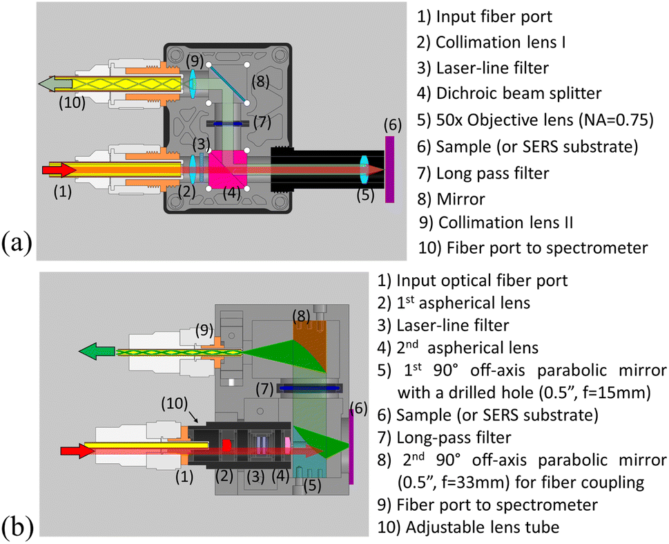 | ||
| Fig. 1 The systematic chart of (a) μ-Raman and (b) RR system. | ||
In contrast, the incident light path of the focusing laser spot (Fig. 1b) and the collection light path by the parabolic mirror in our RR system is decoupled. The input 532 nm laser is carefully aligned with the optical axis and passes through a drill hole on the first parabolic mirror. Although there is a 3 mm diameter drill hole on the surface of the parabolic mirror, the reflection area remains larger than 94.4% (=(3/12.7)2). After passing through the drill hole, the ray reaches the measurement surface (#6) at the focal plane. Moreover, the parabolic mirror collects the Raman scattered light and reflects collimated in a 90° direction of its original optical axis. Finally, the light passes through a longpass filter (#7) and is focused by the second parabolic mirror (#8) into a 400 μm core fiber (#9) to the Raman spectrometer (BWTEK, BTC661E). Separating two light paths allows us to freely decide the incident light spot on the measurement surface by adjusting the distance between two aspherical lenses (#2 and #4). The distance of the first lens (p1) from the end face of the fiber laser and the distance between the two aspherical lenses (d) is 6 mm and 50.51 mm, respectively. Based on the image formation equation in geometric optics, the theoretical spot size is in the range of 2.22–2.78 times the core size of the fiber laser, as shown in Table S1.† In this article, we used 105 μm multimode fiber to get a larger focal spot and lower power density. The magnification is 2.62, which means the theoretical spot size is 275 μm (=105 × 2.62). Moreover, all the optical components to build the RR system are listed in Table S2.†
2.2 Procedure of sample detection
The silicon we used in the experiment is a flat silicon without doping bought from mesophotonics (Klarite sCAL), which is a calibration standard for laboratory instrument comparison. We utilized the silicon standard to assess the uniformity and system stability. All Raman measurements were conducted under identical conditions using a home-built μRaman and RR system. The detailed setup of home-built μRaman system included a fiber-coupled laser (BWTEK, BWN-532-50E), a spectrometer (BWTEK, BTC661E), a Raman probe (BWTEK, BAC101), and an upright microscope (Whited WM-100). The 532 nm diode-pumped solid-state (DPSS) laser served as the excitation source. The laser beam was focused using a 50× (NA 0.75) objective lens, resulting in a 10 mW, 38 μm diameter spot on the SERS substrate, corresponding to a power density of 0.88 kW cm−2. The spectrum integration time was set to 1 second, averaged over ten repetitions.3 Results and discussion
3.1 Optical design and simulations
We simulated the optical path of the RR system by TracePro software and analyzed the diameter of the focusing spot on the sample surface and the collection fiber endface, as shown in Fig. 2. The ratio of the diameter of the two spots is 2.16 (=650 μm/300 μm), which consistent with the focal length ratio 2.2 (=33 mm/15 mm) of our optical design. Moreover, we also measured the diameter of the focusing laser spot on the sample surface by the μ-Raman and the RR system. The results shown in Fig. 3 indicate the diameter of the focusing spot on the sample surface of μ-Raman and our RR system is 38 μm and 278 μm, respectively. Based on the spot size, the power density of the RR system is about 60 times lower than the traditional μ-Raman system (Fig. 3a), which is beneficial to be applied to low damage threshold samples, such as polymer SERS substrate and some thermal sensitive analytes. Fig. 3b indicates the comparison of Raman spectra of 10−6 M Rhodamine 6G (R6G) dried on polymer SERS substrate under the same incident power (10 mW) measured in both μ-Raman and RR systems, the RR system showing the best signal strength of all. The reason is due to the thermal-induced damage to the analyte, which makes the Raman signal decay with time (see Fig. S1†).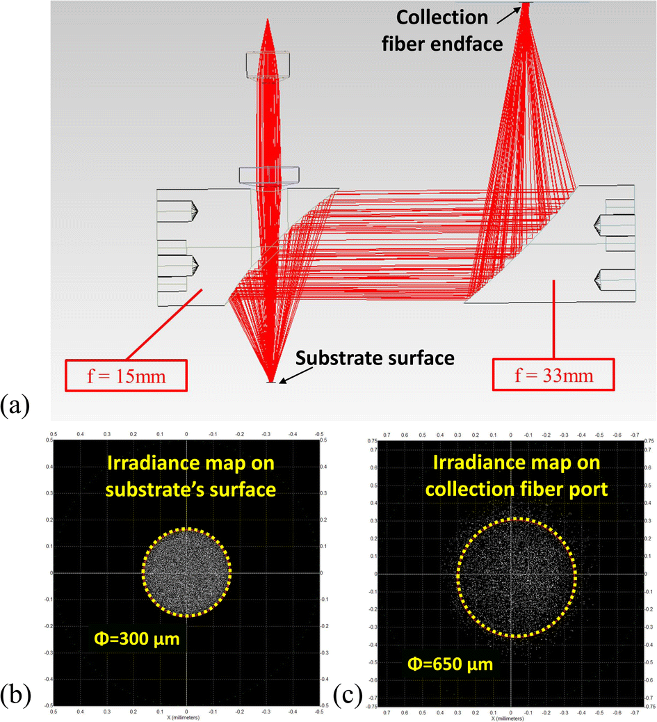 | ||
| Fig. 2 (a) Ray tracing diagram of the RR system and the focusing spot on (b) sample surface and (c) collection fiber end face. | ||
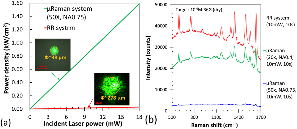 | ||
| Fig. 3 (a) The relationship between incident power and the corresponding incident power density and (b) Raman spectra of R6G measured by μ-Raman and our RR system by 10 mW incident laser power. | ||
Finally, we integrated all the optical components, a manual XY stage by the 3D printed frame structures to build the RR system, as shown in Fig. 4a and S2,† and checked the system stability. Here, we took a silicon wafer as the test sample and measured the time variations (Fig. 4b) and position variations (Fig. 4c) spectra. The coefficient of variation (CV) of the silicon peaks of both systems is less than 0.6% due to the laser source's intensity variation. Moreover, for position variations of five different measurement points within a 2 × 2 cm2 area, the CV of the RR system is less than 0.5%, even better than the μ-Raman system (2.5%), indicating the great benefit of uniform measurement for the large measurement spot and extend the depth of focus.
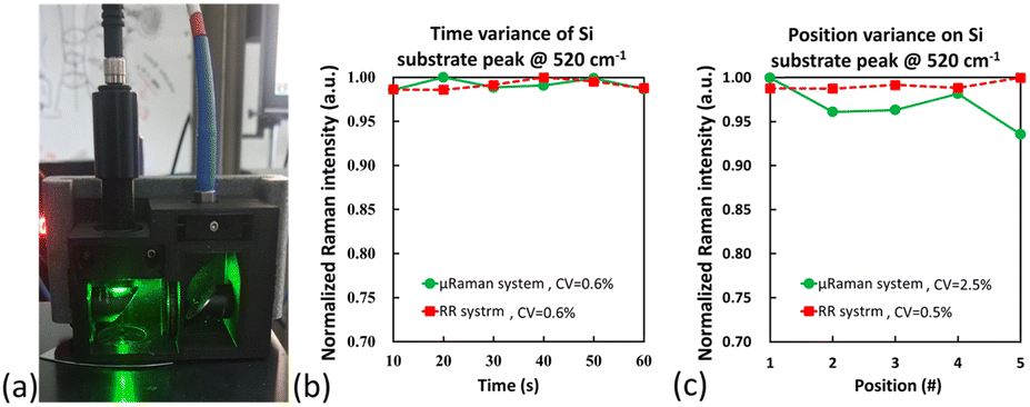 | ||
| Fig. 4 (a) Photo of the RR system and the comparison of (b) time variations and (c) position variations of the RR and μ-Raman system. | ||
3.2 Damage threshold for polymer SERS substrate
To demonstrate the benefit of the low power density RR system, we monitored the Raman peak of the SERS substrate at 1605 cm−1 at different incident power densities. The test sample is a SERS substrate made by a polymer nanostructure substrate covered with a 30 nm silver film deposited by an E-gun evaporator.21 The experimental results of both μ-Raman and RR systems are shown in Fig. 5. The red line shows a rapid drop after the power density exceeds 0.15 kW cm−2, which implies the damage threshold of this polymer SERS substrate. We also found a clear damage mark at the position of the focusing spot area after the incident power density exceeds 0.15 kW cm−2, as shown in Fig. 5b and c. Moreover, we found the slope of our RR system is larger than the traditional μ-Raman system. This is because of the huge difference in power density in both systems. Consequently, if the maximum allowable measurement power density is limited by the analyte (such as polymer SERS substrate, ancient painting, or explosive materials), the best Raman signal of the RR system will always be greater than the μ-Raman system.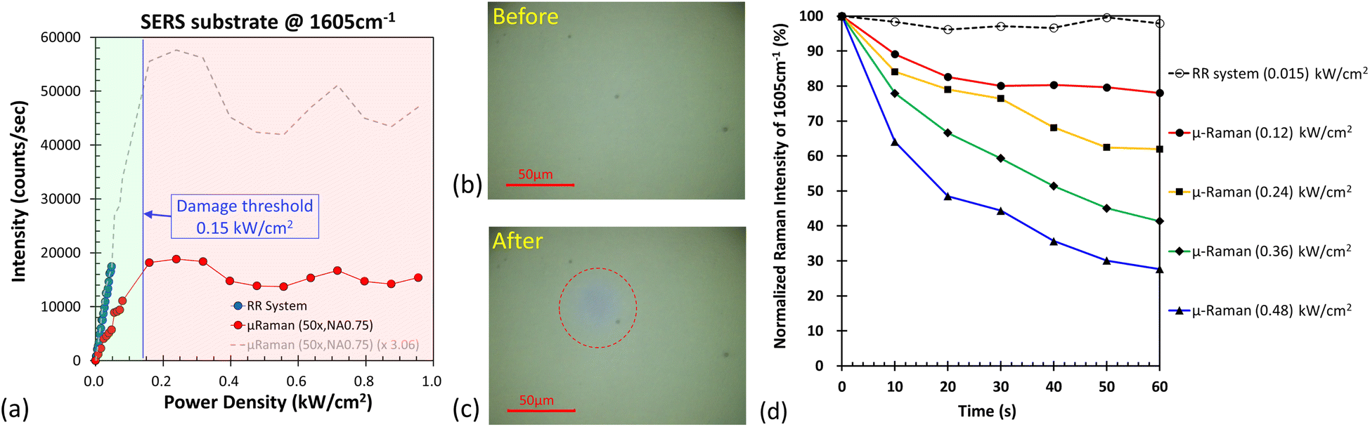 | ||
| Fig. 5 (a) Power density versus Raman peak intensity at 854 cm−1 of the polymer SERS substrate. The surface image of SERS substrate (b) before and (c) after measurement, under the incident power density exceeds 0.15 kW cm−2. (d) The relation of normalized Raman intensity to irradiation time for different input power density conditions of 1605 cm−1 peak on polymer SERS substrate by the conventional μ-Raman system (50×, NA 0.75) and the RR system. | ||
Moreover, based on the regression line calculation in the linear region before 0.15 kW cm−2 of both systems (Fig. S3†), our RR system provides about three times the Raman signal under the same power density input. Due to the limitation of the maximum laser power of our 532 nm laser, we can't see the entire damage threshold trend in our RR system. We multiply the data of the μ-Raman system by a factor of 3.06 to predict the possible trend, as shown in the dashed grey line in Fig. 5a.
3.3 Benefits of low damage threshold reflective Raman system
Fig. 5d indicates the relation of normalized Raman intensity to different input power density conditions of 1605 cm−1 peak on polymer SERS substrate by the conventional μ-Raman system and our RR system. When the input laser power density energy exceeds the damage threshold of the SERS substrate, the Raman signal decays with time, which means we can no longer get a better signal-to-noise ratio by increasing integration time. On the other hand, the RR system has a much lower power density (∼0.015 kW cm−2), and the Raman signal of the analytes on the SERS substrate is time-invariant, as shown in the dashed line of Fig. 5d. Therefore, the RR system is more stable. The best condition for Raman spectrum measurement is under the optimal input laser power density, which is a little smaller than the sample's damage threshold.Moreover, the damage phenomena include not only the dropping of the signal intensity but also the emergence of unexpected or shifting Raman peaks. In Fig. 6, we demonstrated the raw Raman spectra of different input power of both μ-Raman and RR systems and analyzed the characteristic peaks in 857 cm−1, 1133 cm−1, 1279 cm−1, 1394 cm−1, 1607 cm−1, and 1728 cm−1. The vertical black dashed line in Fig. 6 indicates the Raman peak at the incident laser power of 1 mW. We found apparent peak position changes or broadening for the conventional μ-Raman system at 1279 cm−1, 1394 cm−1, and 1607 cm−1. The intensities of Raman signals are not proportional to the incident laser power. On the contrary, the Raman peak positions of our RR system remain the same, and the Raman signals increase linearly with the incident laser power. This phenomenon is significant for qualitative and quantitative analysis. Since, in most cases, we do not know the damage threshold of the sample to be tested initially.
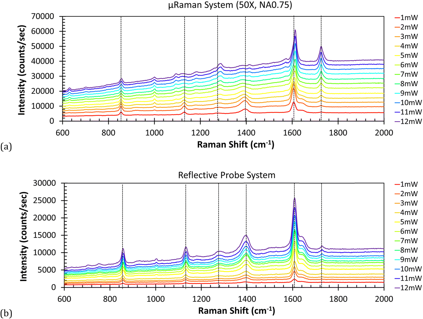 | ||
| Fig. 6 The background Raman spectra of polymer SERS substrate under different input laser power by (a) conventional μ-Raman system (50×, NA 0.75) and (b) our reflective Raman system. | ||
4 Conclusions
In this research, we proposed a novel RR system with a significantly lower power density and high collection efficiency. We compared it with the regular μ-Raman system in many aspects. Due to the common light path design in the regular μ-Raman system, the larger the NA value of the objective lens, the smaller the light spot on the sample surface. This is not ideal for some vulnerable ancient samples or polymer SERS substrates with poor thermal conductivity and low damage threshold. Consequently, our RR system's incident and collection light paths are separated via an off-axis parabolic mirror with a drilled hole. This component gave us complete freedom of control over the focusing spot size and collection cone angle. Finally, the RR system is fulfilled by ray tracing simulations and 3D printing frame structure. However, there is a tradeoff between low power density (large focal spot) and spatial resolution. Typically, the μ-Raman system is more suitable for Raman mapping. But if one wants to minimize the focal spot size on the RRP system, one can also replace it with a single-mode fiber laser. The typical single-mode fiber core size is about 3–5 μm diameter.In short, the RR system can gain about three times signal intensity compared with the μ-Raman system (50×, NA = 0.75) under the same power density input. This shows a much superior measurement performance against the μ-Raman system since either the analyte (or the SERS substrate) has its damage threshold. If the incident power density exceeds the damage threshold, the sample (or the SERS substrate) may cause irreversible change. In addition, heat-induced shifted Raman peaks also lead to incorrect qualitative and quantitative analysis. We found that when the incident laser power exceeds the sample damage threshold, the Raman signal decreases dramatically with time, some unexpected Raman peaks appear, and the original Raman peaks are shifted. We also compared the stability of the RR system with the traditional μ-Raman system. The results show that our RR system has high stability in terms of time variation (CV < 0.6%) and position variation (CV < 0.5%). Based on the advantages of low power density, high efficiency, and high stability, the RR system will be more suitable for all kinds of SERS substrates and low damage threshold analytes, accelerating the development of the SERS technique.
Data availability
The data supporting this article have been included as part of the ESI.†Author contributions
Lin Ding-Zheng: conceptualization, validation, formal analysis, investigation, resources, project administration, writing – original draft; Heng-I. Chang: validation, investigation, visualization, formal analysis; Kai-Chun Tsia: investigation, software, formal analysis; Yu-Ya Chung: investigation.Conflicts of interest
There are no conflicts to declare.Acknowledgements
This work was financially supported by the National Science and Technology Council (MOST 111-2221-E-011-123-MY2), Taiwan. Moreover, we sincerely appreciate the technical guidance from Professor Juen-Kai Wang at the atomic and molecular sciences institute of Academia Sinica and Professor Tsung-Xian Lee at the Graduate Institute of Color and Illumination Technology of National Taiwan University of Science and Technology.References
- J. R. Ferraro, K. Nakamoto and C. W. Brown, in Introductory Raman Spectroscopy, ed. J. R. Ferraro, K. Nakamoto and C. W. Brown, Academic Press, San Diego, 2nd edn, 2003, pp. 1–94 Search PubMed.
- K. Brzozowski, E. Matuszyk, A. Pieczara, J. Firlej, A. M. Nowakowska and M. Baranska, Biotechnol. Adv., 2022, 60, 108003 CrossRef CAS PubMed.
- C. Zong, M. Ge, H. Pan, J. Wang, X. Nie, Q. Zhang, W. Zhao, X. Liu and Y. Yu, RSC Adv., 2019, 9, 2857–2864 RSC.
- Y. Wang, Z. Wang, C. Chen, J. Liu, J. Lu and N. Lu, Anal. Chem., 2023, 95, 14184–14191 CrossRef CAS PubMed.
- H. Dang, S. Park, Y. Wu, N. Choi, J. Yang, S. Lee, S. Joo, L. Chen and J. Choo, Adv. Funct. Mater., 2021, 31, 2105703 CrossRef CAS.
- X.-D. Tian and Y. Zhang, Nanoscale, 2023, 15, 4317–4324 RSC.
- X. Wang, S.-G. Park, J. Ko, X. Xiao, V. Giannini, A. M. Stefan, D.-H. Kim and J. Choo, Small, 2018, 39, 1801623 CrossRef PubMed.
- Y. Wu, H. Dang, S.-G. Park, L. Chen and J. Choo, Biosens. Bioelectron., 2022, 197, 113736 CrossRef CAS PubMed.
- S. A. Kara, A. Keffous, A. M. Giovannozzi, A. M. Rossi, E. Cara, L. D'Ortenzi, K. Sparnacci, L. Boarino, N. Gabouze and S. Soukane, RSC Adv., 2016, 6, 93649–93659 RSC.
- B. S. Lee, D. Z. Lin, C. H. Huang and T. J. Yen, J. Raman Spectrosc., 2018, 49, 1920–1927 CrossRef CAS.
- T. Kang, S. Hong, Y. Choi and L. P. Lee, Small, 2010, 6, 2649–2652 CrossRef CAS PubMed.
- J. Lombard, T. Biben and S. Merabia, J. Phys. Chem. C, 2017, 121, 15402–15415 CrossRef CAS.
- J. Yue, Y. Shen, L. Liang, X. Guan, X. Zhang, S. Xu, C. Liang, W. Shi and W. Xu, Analyst, 2019, 144, 5521–5527 RSC.
- G. Chen and J. Bi, Optik, 2017, 131, 917–924 CrossRef CAS.
- G. Moretti and C. Gervais, J. Raman Spectrosc., 2018, 49, 1198–1204 CrossRef CAS.
- Y. Li, A. Suzuki, C. S. Cheung, Y. Gu, S. Kogou and H. Liang, Eur. Phys. J. Plus, 2022, 137, 1102 CrossRef CAS PubMed.
- A. A. Mencaglia, I. Osticioli and S. Siano, Measurement, 2018, 118, 372–378 CrossRef.
- I. Osticioli, A. A. Mencaglia and S. Siano, Sens. Actuators, B, 2017, 238, 772–778 CrossRef CAS.
- A. A. Mencaglia, I. Osticioli, D. Ciofini, L. Gallo and S. Siano, Rev. Sci. Instrum., 2019, 90, 053101 CrossRef PubMed.
- H. J. H. Chen, L.-C. Chen, C. Lien, S.-R. Chen and Y.-L. Ho, Microelectron. Eng., 2008, 85, 1561–1567 CrossRef CAS.
- C.-H. Lee, C.-H. Tsai and D.-Z. Lin, Spectrochim. Acta, Part A, 2024, 306, 123563 CrossRef PubMed.
- D. Z. Lin, Y. P. Chen, P. J. Jhuang, J. Y. Chu, J. T. Yeh and J.-K. Wang, Opt. Express, 2011, 19, 4337 CrossRef CAS.
- C. Zhang, P. Yi, L. Peng, X. Lai, J. Chen, M. Huang and J. Ni, Sci. Rep., 2017, 7, 39814 CrossRef CAS PubMed.
- V. Suresh, L. Ding, A. B. Chew and F. L. Yap, ACS Appl. Nano Mater., 2018, 1, 886–893 CrossRef CAS.
Footnote |
| † Electronic supplementary information (ESI) available. See DOI: https://doi.org/10.1039/d4ra03874f |
| This journal is © The Royal Society of Chemistry 2024 |