DOI:
10.1039/D4RA03742A
(Paper)
RSC Adv., 2024,
14, 23802-23815
Innovative synthesis, structural characteristics, linear and nonlinear optical properties, and optoelectric parameters of newly developed A2ZnGeO4 (A = K, Li) thin films
Received
21st May 2024
, Accepted 15th July 2024
First published on 29th July 2024
Abstract
The synthesis of high-quality thin films through spin coating deposition on meticulously cleaned glass substrates is presented. Optical band gaps Eg of both samples using the Kubelka–Munk function are determined. The data analysis uncovers the presence of optical allowed direct transition for A2ZnGeO4 (A = K, Li). Spectroscopic ellipsometry measurements on A2ZnGeO4 (A = K, Li) thin films and an analysis of their optical properties using the Cauchy model are presented. Furthermore, the increase of the thickness of the thin film results in improvements in their optoelectrical parameters, such as electrical conductivity, optical mobility, and optical conductivity. Using the Kubodera and Kobayashi comparative model, the third order nonlinear susceptibility (χ(3)) was estimated based on the compounds' high linear absorption of the generated third harmonic wavelength (355 nm). This paper presents remarkable NLO results that reveal potential uses in optoelectronics and photonics.
1. Introduction
In the past, researchers and scientists have focused their research on quaternary thin films as a promising absorber layer for solar cell applications. However, the high production costs associated with these thin films have prompted researchers to seek out a novel, more cost-effective alternative. This new family, known as chalcopyrite materials, is formulated as CuABX4, where A represents either Ga or In, B represents Ge or Sn, and X represents Se or S. Chalcopyrite materials present themselves as an attractive option for thin-film solar cells due to their favorable electrical and optical properties. Consequently, three compositions are available to researchers for the fabrication of absorbing thin-film solar cells: CuInGeSe4, CuInGeS4, and CuGaGeSe4. In previous research works, these films have demonstrated that they are excellent absorber layers.1,2 Additionally, there is also another interesting quaternary family, based on the structure of A2MCX4, where A is (Ag or Cu), M is (Zn or Mn or Cd), C is (Ge or Sn), and X is (Se or S). Kesterite materials, such as Cu2ZnSnS4 (CZTS) and Cu2ZnSnSe4 (CZTSe), are promising candidates for thin-film solar cell applications due to their suitable optical and electrical properties. Thin films of kesterite based on copper have attracted significant attention because of their unique and intriguing electrical, optical, and optoelectronic properties.3,4 These semiconducting samples have a high absorption coefficient and high thermal stability. These distinctive characteristics make these quaternary samples suitable for various applications, like absorber layers for solar cells, optical memory devices, photodetectors, and IR sensors.5,6 The electrical properties of kesterite materials are also favorable for photovoltaic applications. They have relatively high p-type conductivity, which is essential for forming a p–n junction with an n-type buffer layer, such as CdS. The carrier concentration and mobility can be tuned by controlling the composition and defects in the kesterite structure. Cu2MnGeS4 optical conductivity and nonlinear optical parameters, including the nonlinear refractive index and third-order susceptibility, were investigated. These excellent optical results strongly encourage the use of these films in a wide range of possible optical applications, particularly in solar cells where they serve as an excellent absorber layer for thin-film solar cells. The aim of the present research is to prepare a quaternary family of thin films based on the structure of A2ZnGeO4, where A is (K or Li), using the spin coating deposition technique for the first time. The authors have tried to prepare these novel film samples to have a good quality and optical properties comparable to those of similar thin films. Subsequently, the authors investigated and discussed the linear and nonlinear optical properties and some optoelectrical variables of these samples. As far as we know, there is no work that discusses the fabrication and study of the optical properties of the A2ZnGeO4 thin films. Consequentially, the authors considered that it was difficult to refer to previous published literature. However, they changed this consideration by presenting their obtained results with comparable studies in which their compounds are identical to the current materials of this research.
2. Experimental
2.1. Preparation of a powder samples
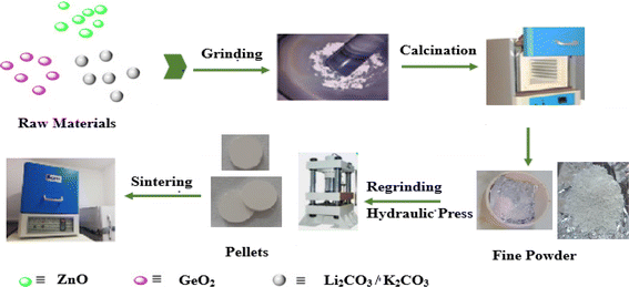
A2ZnGeO4 (A = K+, Li+) compounds were synthesized by means of the conventional high-temperature solid-state reaction method. ZnO (Sigma-Aldrich, 99%), GeO2 (Sigma-Aldrich, 99%), and the oxides (Li2CO3, K2CO3) (Sigma-Aldrich, 99%) were the starting materials that were synthesized. They were carefully weighed, pulverized in an agate mortar, and then calcined at 400 °C for 15 hours to remove CO2. In the goal to boost the reaction, the powders were compressed into pellets with an 8 mm diameter at a pressure of 3 tons per cm2. After that, the powder was heated for 15 hours at 1123 K for K2ZnGeO4 and 1073 K for Li2ZnGeO4. Fig. 1 shows how these samples were synthesized.
 |
| | Fig. 1 Schematic diagram of synthesis of A2ZnGeO4 (A = K, Li) compounds. | |
2.2. Preparation of a thin films
After using ultrasonic to clean the glass substrates using a commercial surfactant, deionized water was used to rinse them multiple times. The substrates were then annealed for three hours at 100 °C in an oven to finish the purification process. After that, one milliliter of dimethyl sulfoxide was used to dissolve the powdered forms of both chemicals. The thin films of both samples were then produced by centrifuging a single drop onto the substrate for 60 seconds at 2000 rpm. The last stage involved annealing the films for five hours at 110 °C in an oven.
2.3. Apparatus
The synthesized compounds were characterized using various methods. These included X-Ray Diffraction (XRD) pattern to assess the purity of the crystalline phases, energy Dispersive X-ray (EDX) to confirm the chemical composition, and scanning electron and transmission electron microscopy for analyzing morphology and particle size distribution. Raman spectra of A2ZnGeO4 (A = K, Li) samples were acquired using a Raman spectrometer (DXR, Thermo Fisher Scientific, USA). Optical characteristics like absorbance spectra, bandgap energy, and Urbach energy were investigated. Spectroscopic Ellipsometer–UVISEL, HORIBA was employed to explore other optical properties, such as the refractive index and the extinction coefficient. Finally, the nonlinear optical properties that have been presented have been measured with an emphasis on determining the nonlinear optical susceptibility χ(3) of various thin films in order to comprehend their possible uses in highly nonlinear photonic systems.
3. Results and discussion
3.1. XRD analysis
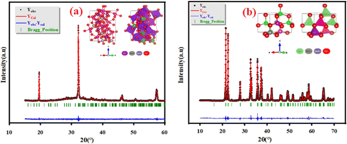
The Panalytical X'Pert Prompd was utilized for X-Ray Diffraction (XRD) analysis of K2ZnGeO4 and Li2ZnGeO4 compounds. The X-Ray Diffraction (XRD) measurements were conducted at room temperature in the 2θ range of (10–60)° for K2ZnGeO4 and (10–70)° for Li2ZnGeO4 using a Cu-Kα source, as shown in Fig. 2(a) and (b). The structures of these compounds are represented in the inset of Fig. 2(a) and (b). The crystal structures of A2ZnGeO4 (A = Li and K) materials were refined with Rietveld method using the FULLPROF program. The gained results of the Rietveld refinement are collected in Table 1. In the previous studies, we discussed X-ray diffraction in detail.7,8
 |
| | Fig. 2 XRD patterns of as-prepared (a) K2ZnGeO4 and (b) Li2ZnGeO4 compounds. | |
Table 1 Crystal data for A2ZnGeO4 (A = Li and K) compounds
| Compound |
System/space group |
The refinement parameters |
| Li2ZnGeO4 |
Monoclinic |
a (Å) = 6.36/b (Å) = 5.43/c (Å) = 5.03/β (°) = 90.19 |
| Pn |
Rp (%); Rwp (%); RB (%): RF (%) = 9.81, 11.2, 2.23, 2.88 |
| |
χ2 = 2.81 |
| K2ZnGeO4 |
Orthorhombic |
a = 11.128 (5)/b = 5.539 (2)/c = 15.828 (6), α = β = γ = 90° |
| Pca21 |
Rp (%); Rwp (%); RB (%): RF (%) = 11.9, 12.2, 2.67, 4.56 |
| |
χ2 = 1.28 |
3.2. Morphological characterization and particle size distribution determined by SEM and TEM
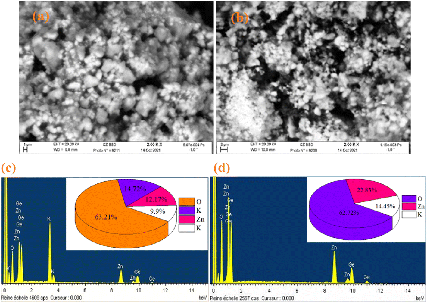
The SEM and EDX techniques were utilized to analyze the composition and structure of our samples. These two techniques detected elements in the compounds by observing backscattered electrons. In Fig. 3(a) and (b), the images exhibit a combination of small and large grains evenly dispersed in the two compounds. Notably, there is agglomeration, likely caused by moisture due to the presence of lithium and potassium. The EDX spectra in Fig. 3(c) and (d) indicate the presence of various elements like oxygen, zinc, potassium, and germanium. It is worth mentioning that lithium is not visible in Fig. 3(d) as it shares the same atomic number as the reference element beryllium used for these compounds. To further analyze the particle size distribution, a transmission electron microscopy (TEM) was used, and the results are shown in Fig. 4(a) and (b).
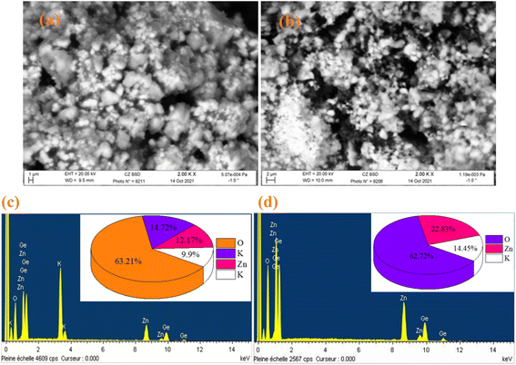 |
| | Fig. 3 SEM image of K2ZnGeO4 (a) and Li2ZnGeO4 (b), along with the elemental analysis by EDX of K2ZnGeO4 (c) and Li2ZnGeO4 (d). | |
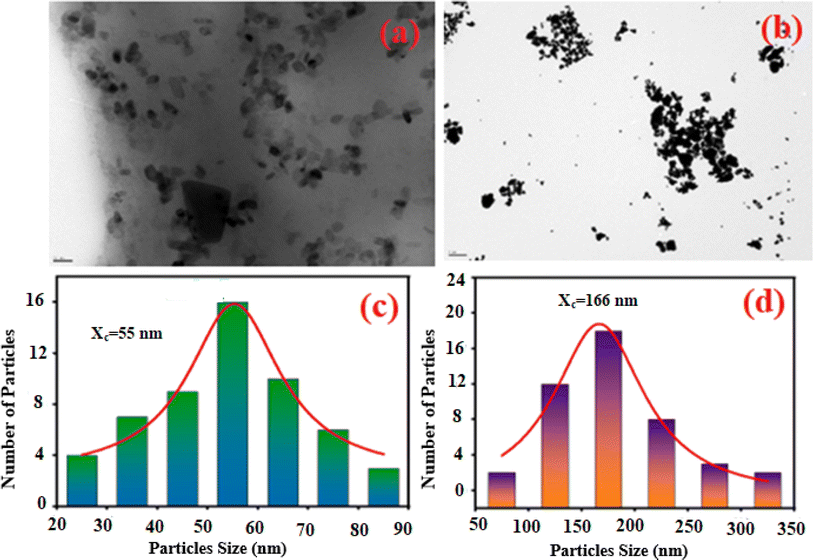 |
| | Fig. 4 The TEM image of K2ZnGeO4 (a) and Li2ZnGeO4 (b) along with the particle size distribution of K2ZnGeO4 (c) and Li2ZnGeO4 (d). | |
ImageJ software was used as for statistical analysis of grain size on TEM images. The results are illustrated as histograms in Fig. 4(a) and (b), depicting counts (grain number) versus particle sizes. These histograms indicate that the particle sizes obtained are mainly within the range of 20–90 nm for K2ZnGeO4 and 50–350 nm for Li2ZnGeO4 (Table 2).
Table 2 Observed Raman for K2ZnGeO4 and Li2ZnGeO4 and the bands assignment
| Compound |
Assignment |
| Li2ZnGeO4 |
K2ZnGeO4 |
| 118.51 |
102.88 |
External modes vibrations |
| 130.45 |
139.85 |
| 181.24 |
180.85 |
| 192.67 |
196.48 |
| 206.88 |
248.28 |
| 242.57 |
317.83 |
| 269.42 |
362.96 |
| 317 |
|
| 328.83 |
|
| 365.84 |
|
| 390.52 |
405 |
δs (GeO4) |
| 427.08 |
|
| 441.55 |
|
| 468.44 |
465.72 |
δas (GeO4) |
| 482.71 |
520.59 |
νs (GeO4) |
| 494.62 |
580.58 |
| |
615 |
| |
661.93 |
| 708.30 |
747.52 |
νas (GeO4) |
| 719.73 |
781.30 |
| 751.73 |
801.49 |
3.3. Raman spectra
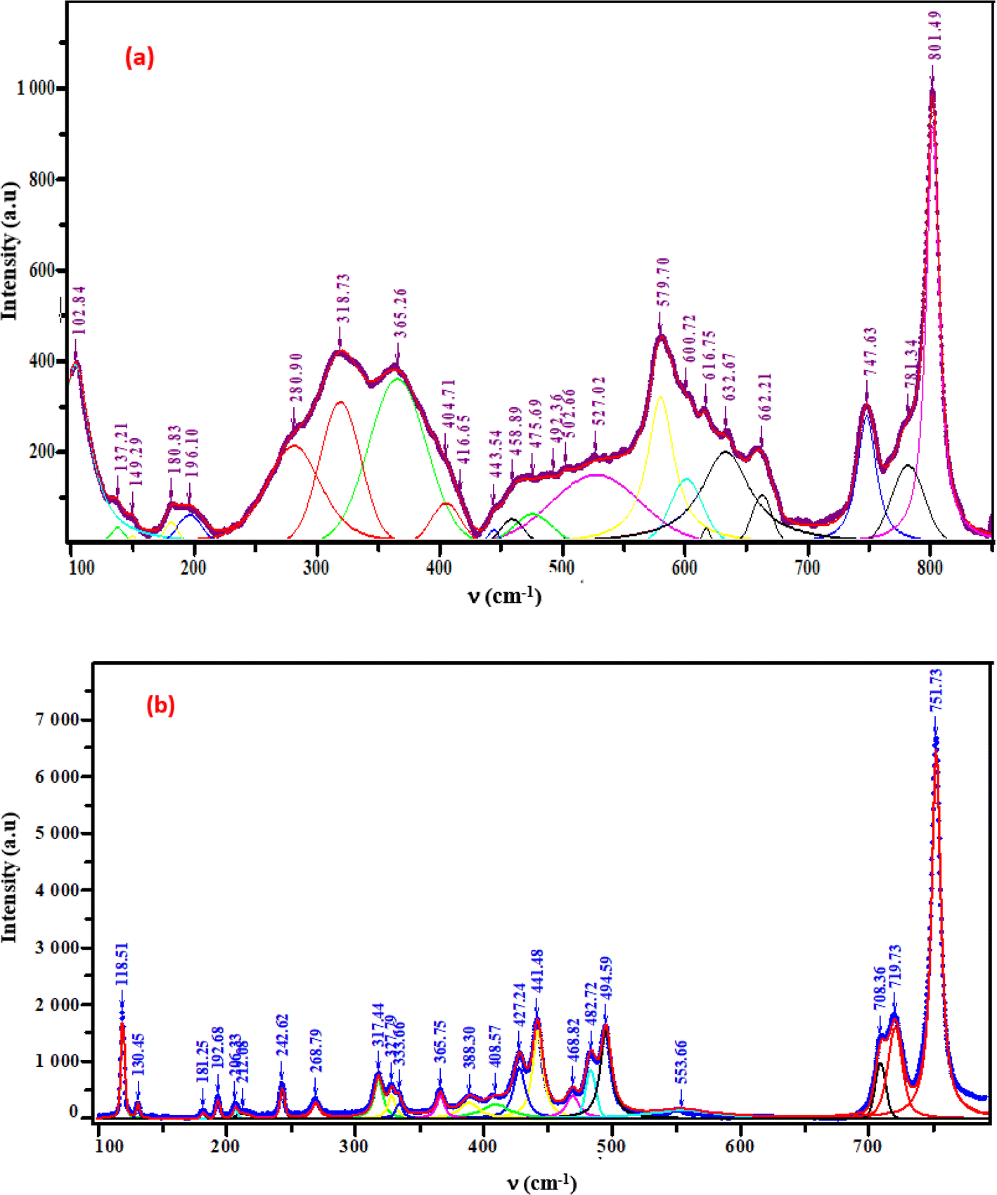
The crystal structures of these samples were analyzed using Raman spectroscopy to confirm the presence of the functional group [GeO4]4−. Measurements were taken at room temperature within the 100–800 cm−1 spectral range. Fig. 5(a) and (b) illustrates the intensity variation of the Raman spectra with respect to wavenumber.9,10 These two samples band assignments are determined based on the similar compounds in the bibliography (given in detail in Table 1).
 |
| | Fig. 5 Raman spectra of the phosphors (a) K2ZnGeO4, (b) Li2ZnGeO4. | |
3.3.1. External modes vibrations. The Raman bands, which are found below 365 cm−1 are related to the external modes. The peaks in this range are linked to translational and librational modes of GeO4 and ZnO4 tetrahedra. Differentiating between translational and vibrational modes is challenging due to limited vibrational studies on similar compounds.
3.3.2. Internal modes vibrations. In A2MGeO4 compounds, the internal modes consist of vibrations within functional groups, such as MOn (n=4, 5, and 6) and GeO4 polyhedra. In A2ZnGeO4 (A = K, Li) compounds, the bonds between Ge and O atoms are stronger than those between Zn and O atoms, resulting in vibrational modes primarily involving the vibrations of the GeO4 tetrahedra. The isolated GeO4 tetrahedra (point group: Td) demonstrate two main types of vibrational modes: bending and stretching. The modes in the 390–850 cm−1 region can be classified into the following frequency classes:
3.3.3. 390–468 cm−1. The symmetric and asymmetric bending modes of O–Ge–O vibration.
3.3.4. 480–801 cm−1. The symmetric and asymmetric stretching modes of O–Ge vibration.
3.4. UV–visible study
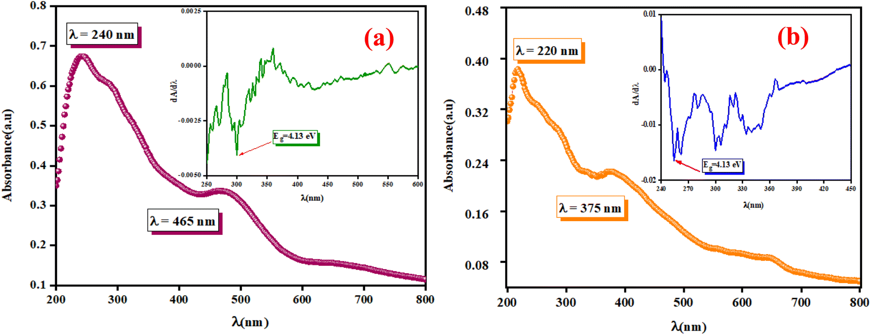
The optical measurements were conducted to estimate the light efficiency of the synthesized compounds A2ZnGeO4 (A = K+, Li+). The absorption spectra were used to determine the main optical properties, such as the optical band gap and the Urbach energy. Fig. 6(a) and (b) displays the absorbance spectra of these samples, which were analyzed in the wavelength range of 200 to 800 nm at room temperature.
 |
| | Fig. 6 The UV-vis absorbance spectrum A (λ) and dA/dλ as a function of λ in the inset for the phosphors K2ZnGeO4 (a) and Li2ZnGeO4 (b) at room temperature, spanning from 200 to 800 nm. | |
These spectra show the presence of the lowest absorption peaks at 240 nm and 220 nm for the K2ZnGeO4 and Li2ZnGeO4 samples, respectively. These peaks are attributed to the absorption of the highest energy level in the conduction band. Notably, these compounds display a broad emission band spanning from 350 to 550 nm, indicating the recombination of donors ( and
and  ) and acceptors
  due to intrinsic defects in the host lattice at elevated temperatures.11
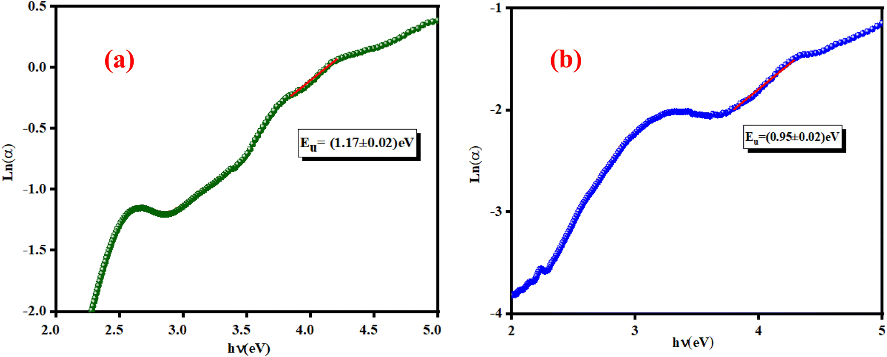
3.4.1. Determination of the optical band gap Eg. The optical band gap (Eg) can be directly determined from the minimum points of the dA/dλ curves, as shown in the inset of Fig. 6(a) and (b). The optical band gap (Eg) values are 4.13 eV and 4.7 eV for the K2ZnGeO4 and Li2ZnGeO4 samples, respectively. The band gap energy was also calculated also according to the Tauc's law and is given by the following equation:12In eqn (1), the parameter denoted by the interband transition probability is A. The incident energy is represented as hν. Eg represents the energy band gap, and the index n specifies the type of electron transition. The value of indirect permitted electron transitions (n) was 2, n for direct permitted transition was 1/2, n for indirect prohibited transitions was 3, and for direct prohibited transitions, n was 3/2. Fig. 7(a) and (b) shows the variation of (αhν)2 with photon energy.
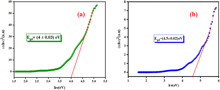 |
| | Fig. 7 Plots of (αhν)2 as a function as hν of (a) K2ZnGeO4 and (b) Li2ZnGeO4. | |
Extrapolating these curves gives direct optical band gap values of Egd = (4 ± 0.03) eV and Egd = (4.5 ± 0.02) eV for the K2ZnGeO4 and Li2ZnGeO4 samples, respectively. It is important to note that, while this method may lack precision, the band-gap values are consistent with previous research. These values fall within the range of wide optical band gap semiconductors, indicating their potential for opto-electronic applications. To determine whether the electron transition type in our compounds is direct or indirect, we rearranged eqn (1) as follows:
| |
ln(αhν) = ln(A) + n![[thin space (1/6-em)]](https://www.rsc.org/images/entities/char_2009.gif) ln(hν − Eg) ln(hν − Eg)
| (2) |
Fig. 8(a) and (b) show the variation of ln(αhν) as a function of ln(hν − Eg). We utilized Eg obtained from Fig. 7(a) and (b) as test values. The slopes of the resulting lines indicate the power factor (n). For these energies, n is around 0.5, validating the direct transition behavior of the compounds studied.
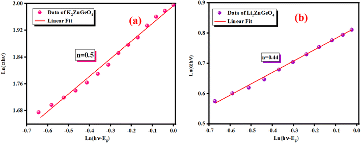 |
| | Fig. 8 Variation of ln(αhν) against ln(hν − Eg) of (a) K2ZnGeO4 and (b) Li2ZnGeO4. | |
3.5. Ellipsometric investigation of A2ZnGeO4 (A = K, Li)
Spectroscopic ellipsometry (SE) is a technique to measure the changes in polarization of light as it reflects off a surface. Ellipsometry refers to the fact that linearly polarized light changes its polarization state to elliptical polarization when reflected at an oblique angle, hence the term “ellipsometry”.14 Spectroscopic ellipsometry (SE) was used to determine various parameters of thin films, including the optical extinction coefficient, refractive index, optical conductivity, and dispersion energy parameters. Cauchy's empirical correlation between wavelength and refractive index was also employed.
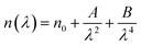
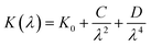
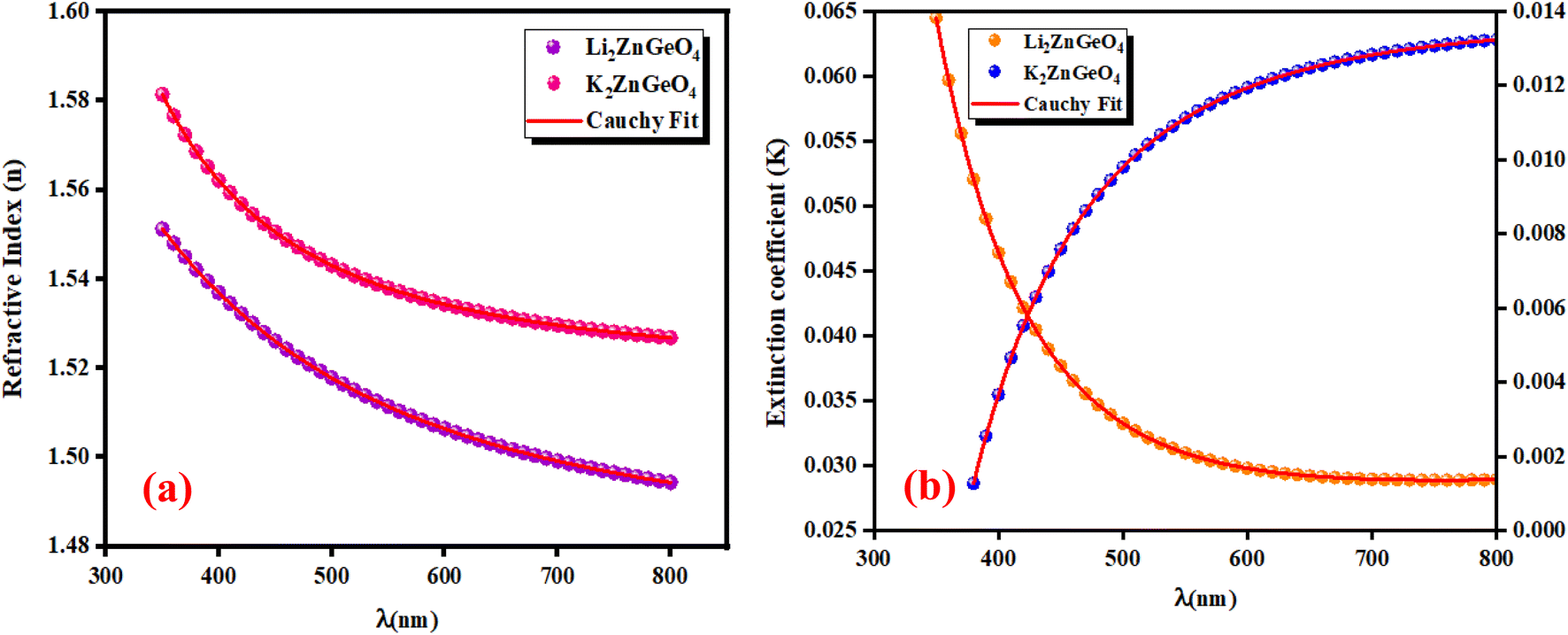
3.5.1. Refractive index and extinction coefficient of the films. Fig. 10(a) and (b) presents the refractive index (n) and extinction coefficient (K) of A2ZnGeO4 (A = K, Li) thin films depending on the wavelength range of 300 to 800 nm. We can observe in Fig. 10(a) and (b) that the refractive index (n) for all samples decreases when the wavelength increases. While the extinction coefficient (K) increases for K2ZnGeO4 and decreases for Li2ZnGeO4 as the wavelength increases. This phenomenon is attributed to light scattering and a decrease in absorbance. The refractive index and extinction coefficient varied along the Cauchy distribution in all thin films studied, as described by the following relationships:15| |
 | (4) |
| |
 | (5) |
where A, B, C, and D represent Cauchy's parameters, while λ denotes the wavelength of the light. These parameters are summarized in Table 3. The refractive index values of all samples are lower compared to the theoretical refractive index in the visible region (n = 2). Additionally, the extinction coefficient value is significantly low, suggesting that the A2ZnGeO4 (A = K, Li) films exhibit low dielectric loss.16
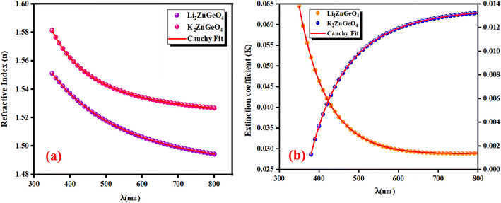 |
| | Fig. 10 Refractive index (a) and extinction coefficient (b) plots versus wavelength for K2ZnGeO4 and Li2ZnGeO4 compounds. | |
Table 3 Cauchy parameters for K2ZnGeO4 (A = K, Li) compounds
| n |
n0 |
A (μm2) |
B (μm4) |
| K2ZnGeO4 |
1.51 |
0.0450 |
0.0387 |
| Li2ZnGeO4 |
1.47 |
0.1096 |
−0.0241 |
|
| K |
K0 |
C |
D |
| K2ZnGeO4 |
0.01 |
0.0015 |
−0.0280 |
| Li2ZnGeO4 |
0.03 |
−0.0304 |
0.0867 |
3.5.2. Dispersion analysis. Furthermore, in addition to the Cauchy extrapolation discussed above, which was done to offer reasonable values for refractive index in the spectral region of low absorption, the dispersion energy was also assessed using the single oscillator model as explained by Wemple and DiDomenico:17| |
 | (6) |
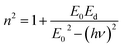
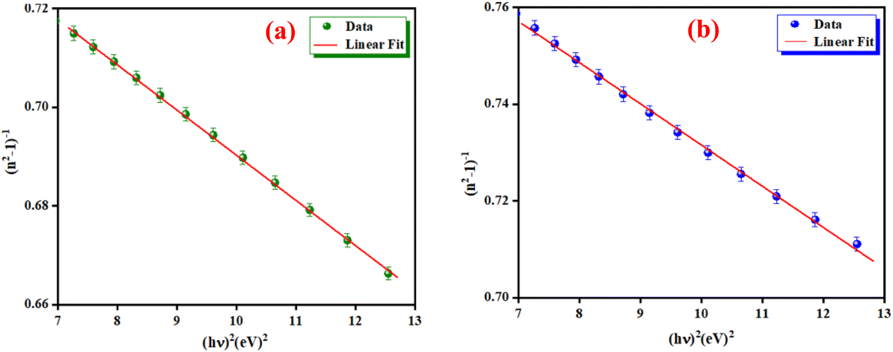
where E0 is called the energy of the effective dispersion oscillator, which is expected to link to the photon-energy location of the ultraviolet band gravity center. The dispersion energy (Ed) is a measurement of the interband optical transition average strength. E0 and Ed can be both determined from the slope (1/E0Ed) and the intercept (E0/Ed), as shown in Fig. 11(a) and (b). Their values are summarized in Table 4.
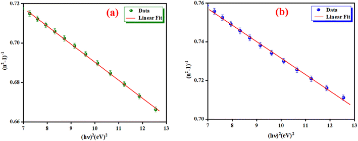 |
| | Fig. 11 The (n2 − 1)−1 as a function of (hν)2 for K2ZnGeO4 (a) and Li2ZnGeO4 (b). | |
Table 4 The optical parameters of the A2ZnGeO4 (A = K, Li) samples
| Thin films |
Thickness (nm) |
E0 (eV) |
Ed (eV) |

|
εs |
f (eV)2 |
λ0 (nm) |
| Li2ZnGeO4 |
91 |
5.75 |
12.87 |
1.79 |
3.20 |
70.14 |
130 |
| K2ZnGeO4 |
97 |
5.02 |
14.64 |
1.97 |
3.88 |
73.49 |
133 |
The Ed and Eo values in thin film analysis are important factors that provide knowledge of the characteristics of the films. Ed denotes the elastic modulus of the film, which represents its stiffness, whereas Eo is related to the optical modulus, which describes how the film interacts with light. As film thickness rises, Ed values generally rise, indicating a higher rigidity, whereas Eo values decrease, indicating modifications in optical properties.18 This finding indicates that the K2ZnGeO4 film is more rigid than the Li2ZnGeO4 film. Furthermore, the oscillator strength (f), the static refractive index  and the static dielectric constant (εs) of the A2ZnGeO4 (A = K, Li) films were estimated using the presented relations:19,20
| |
 | (8) |
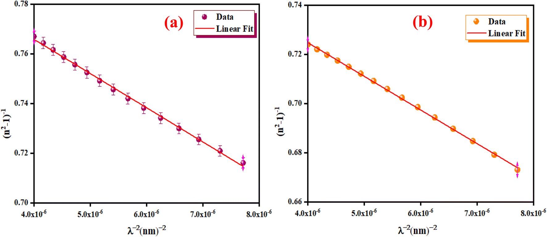
Table 4 shows the magnitudes of the oscillator strength (f), the static refractive index  and the static dielectric constant (εs) of the A2ZnGeO4 (A = K, Li) thin films. It is observed that by increasing the film thickness, the magnitudes of f, n0 and εs were raised. However, these factors are highly dependent on the refractive index measurements, which increase with increasing film thickness. Consequentially, the increased values of these factors (f, n0 and εs) are related to this rise in the refractive index values, and resulted from the enhancement of the crystallization of films, the movement of atoms towards other ones, and their organization in a more stacked manner, in addition to reduce the vacancies and crystal defects. According to the literature, similar findings have been reported for the dispersion parameters of other thin films.21,22 Along with these parameters, we have also calculated, utilizing the same model, the average oscillator wavelength (λ0) for the A2ZnGeO4 (A = K, Li) using the following equation:23
| |
 | (10) |
We have reported in Fig. 12(a) and (b) the plot of (n2 − 1)−1 versus (λ)−2. The values of the average oscillator wavelength (λ0), which we obtained using the linear fit, are listed in Table 3. These values are comparable to the results found for other compounds under study.18
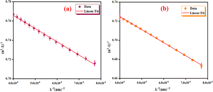 |
| | Fig. 12 The (n2 − 1)−1 as a function of λ−2 for K2ZnGeO4 (a) and Li2ZnGeO4 (b). | |
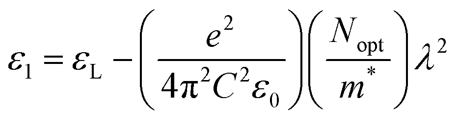
3.5.3. Optoelectrical analysis. The real part (ε1) and the imaginary part (ε2) of the dielectric constant of the A2ZnGeO4 (A = K, Li) films were determined by using the n and k calculations:24,25Fig. 13(a) and(b) shows the variation of the real part (ε1) and the imaginary part (ε2) of the dielectric permittivity as a function of k relative to the A2ZnGeO4 (A = K, Li) films.
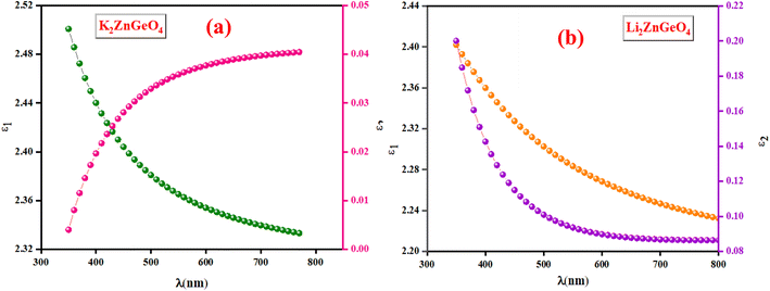 |
| | Fig. 13 The ε1 and ε2 against the λ of the (a) K2ZnGeO4 and (b) Li2ZnGeO4. | |
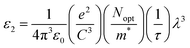
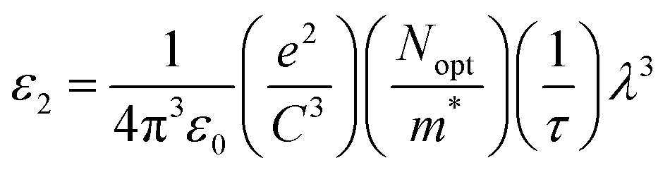
It is interesting to note that the real part of the dielectric constant provides an indication of the light speed being slowed down in the material, whereas the imaginary part is related to how much energy is absorbed from incident light during dipole motion. As previously mentioned, these dielectric parameters also depend on the refractive index values, which rose with increasing film thickness as a result of improved film crystallization, a decrease in atomic interplanar distances, and a reduction in crystal defects and vacancies.26 These excellent results and the performance of the dielectric characteristics reveal the favorable optical response of the present thin films. In addition to these precedent parameters, we have also calculated the charge carrier concentration to effective mass ratio (Nopt/m*), the lattice dielectric constant (εL) and the relaxation time (τ) of the A2ZnGeO4 (A = K, Li) films, which can be evaluated via the following relations:27,28
| |
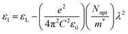 | (13) |
| |
 | (14) |
here
C is the speed of light,
ε0 is the electric permittivity of free space, and
e represents the electronic charge.
Fig. 14(a) shows the reliance of
ε1 on
λ2 for the A
2ZnGeO
4 (A = K, Li) films. The values gained for both (
Nopt/
m*), (
εL) are presented in
Table 4. It is noticed that the ratio
Nopt/
m* increases with increasing film thickness. This suggests that the change in film thickness is associated with an expansion in the charge carrier concentration. It might be related to the increase in the lone-pair electrons of the oxygen (O) atom in the film K
2ZnGeO
4. On the flip side, the values of
εL increase with increasing the film thickness. This result could be explained by the increase in the degree of order in the K
2ZnGeO
4 film, which improves the arrangement of atoms in the film compared to the Li
2ZnGeO
4 film. Furthermore, the relaxation time,
τ, of the A
2ZnGeO
4 (A = K, Li) films was determined (
Table 5). The variation of the imaginary dielectric constant
ε2 as a function of
λ3 for the A
2ZnGeO
4 (A = K, Li) films is displayed in
Fig. 14(b), and we can estimate the relaxation times,
τ, of the studied thin films from the slope of these curves. Additionally, the values of relaxation times,
τ, for the A
2ZnGeO
4 (A = K, Li) thin films were found to decrease with increasing film thickness.
 |
| | Fig. 14 (a) The variation of ε1 with λ2 and (b) The ε2 against λ3 for the A2ZnGeO4 (K, Li). | |
Table 5 The ratio of the charge carrier concentrations to the effective mass (Nopt/m*), The lattice dielectric constant, (εL), time constant, (τ), optical mobility, μopt, optical resistivity, ρopt and the third order susceptibility, χ(3) of the various samples
| Thin films |
Thickness (nm) |
(Nopt/m*) (1047) (kg−1 m−3) |
(εL) |
τ (10−9) (s) |
μopt (10−6) (C s per kg) |
ρopt (kg m3 C−2 s−1) |
χ(3) 10−12 (esu) |
n2 10−12 (esu) |
| Li2ZnGeO4 |
91 |
3.15 |
2.30 |
3.24 |
9.22 |
0.038 |
0.17 |
3.58 |
| K2ZnGeO4 |
97 |
4.59 |
2.38 |
2.10 |
9.53 |
0.040 |
0.49 |
3.76 |
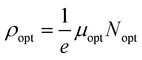
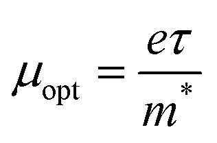
3.5.4. Optical mobility and optical resistivity. In this research, the optical resistivity (ρopt) and the optical mobility (μopt) of the A2ZnGeO4 (A = K, Li) films have been calculated using the following equations:29,30| |
 | (15) |
| |
 | (16) |
The calculated values of both the optical resistivity ρopt and the optical mobility μopt are listed in Table 5 for the current films. It is noted that both the μopt and ρopt values increase as the film thickness increases. These findings are consistent with other published works.31
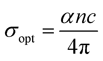
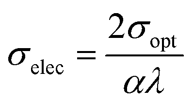
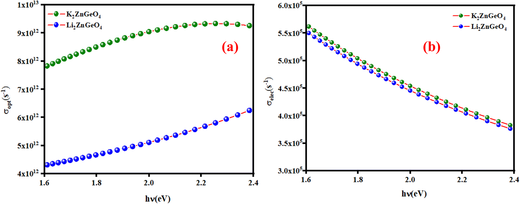
3.5.5. Optical and electrical conductivity analysis. In the present study, the optical conductivity (σopt) and electrical conductivity (σele) of the A2ZnGeO4 (A = K, Li) films were calculated using the below expressions:32| |
 | (17) |
| |
 | (18) |
here, (c) is the speed of light. Fig. 15(a) shows the variation of the opt versus the hν for the A2ZnGeO4 (A = K, Li) samples. From this graph, it can be seen that the values of (σopt) increased as both photon energy and film thickness increased. This trend may be due to increasing electron excitation with increasing photon energy. Furthermore, Fig. 15(b) represent the evolution of the (σele) as a function as the (hν) for the A2ZnGeO4 (A = K, Li) samples. This curve shows that the A2ZnGeO4 (A = K, Li) samples' electrical conductivity rises with increasing film thickness and reduces with increasing photon energy. The elevated values of both (σopt) and (σele) are to decrease the values of stress, crystal defects, and lattice deformations. The decrease of these parameters makes the conductivity greater, which means that electromagnetic radiation moves faster, and electrons circulate more freely and at higher speeds, so the conductivities increase. Previous studies have reported comparable results for the present film samples.21,22
 |
| | Fig. 15 (a) The variation of the optical conductivity and (b) the electrical conductivity versus the photon energy for the A2ZnGeO4 thin films. | |
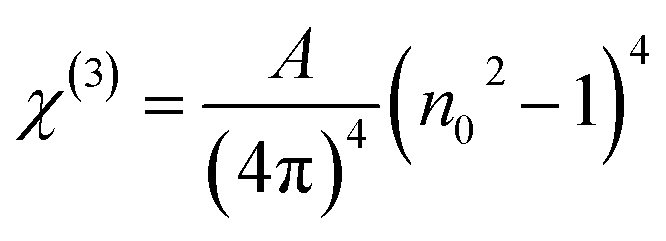
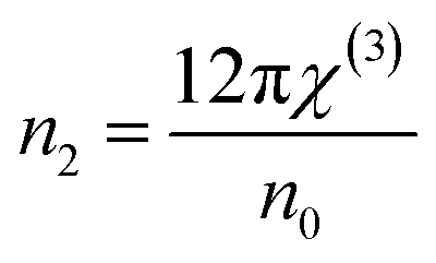
3.5.6. Nonlinear optical characterization. Nonlinear optical factors have received more interest in recent research papers for all studied materials because of their significant applications in optical switching devices, optical signal processing, electro-optic modulators, and optical circuits.33 There are two essential nonlinear factors that can be determined by using semi-empirical equations that primarily depend on the refractive indices of the film. The factors are the third-order nonlinear susceptibility (χ(3)) and the nonlinear refractive index n2. This study used the following Miller's formulas to calculate the magnitudes of the (χ(3)) and n2 for the A2ZnGeO4 (A = K, Li) films:34| |
 | (19) |
| |
 | (20) |
here A is a constant factor equal 1.7 × 10⁻¹⁰ esu. Table 5 displays the values of (χ(3)) and n2 corresponding to the different samples. The increase of the values of (χ(3)) and n2 of K2ZnGeO4 compared to Li2ZnGeO4 is also attributed to the increase of the values of the static refractive index,  , which is a consequence of the change in the refractive index linear, n0, due to the enhancement of crystallization and a reduction in the values of defects in crystals, stresses, and lattice strains that occur in the film materials. Comparable results for these nonlinear optical parameters were reported in earlier works involving similar thin films.35
3.6. Nonlinear optical properties of the A2ZnGeO4 (A = K, Li) thin films
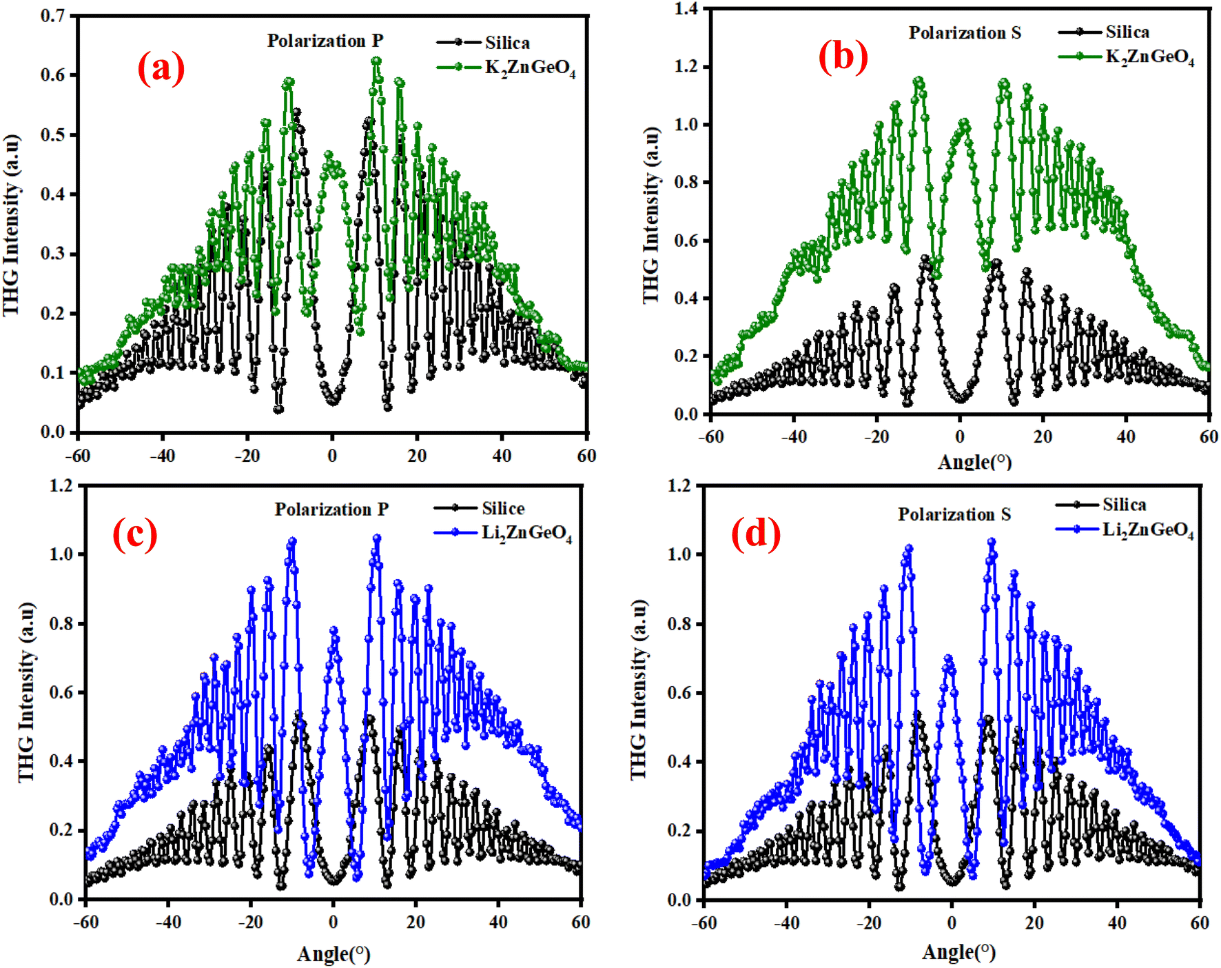
The third-order nonlinear optical susceptibilities (χ(3)) of the A2ZnGeO4 (A = K, Li) thin films were investigated by the THG method. All measurements were performed using the rotational Maker fringe process. The Nd: YAG laser beam (PL2250, Ekspla, Vilnius, Lithuania) with a pulse duration of 30 ps, a wavelength of 1064 nm, a repetition rate of 10 Hz, and a power of 90 μJ, traveling through a group of optical elements, was concentrated on the compound using the lens with a focal distance of 25 cm, and then the compound was rotated by −60° to the point perpendicular to the laser radiation and further rotated to +60°. THG measurements were conducted in two configurations: an s-polarized and p-polarized laser beam, s and p, were obtained by varying the angle on the half-wave plate (λ/2). After applying an interference filter (355 nm), the separated signal was collected by a photomultiplier tube and transformed into graphical data. The reference material for the third harmonic generation measurements was a silica glass plate. UV-vis spectra of the studied thin films are presented in Fig. 16(a) and (b). It should be noted that the absorbance is significant around a wavelength of 355 nm, corresponding to a third harmonic generated. This means that absorption must be taken into account in third-order nonlinear optical susceptibility calculations. To calculate the third-order online optical susceptibility, the Kubodera–Kobayashi model was employed.36| |
 | (21) |
where: χ(3)Silica is the third nonlinear susceptibility of fused silica, d is sample thickness, α represent the linear absorption coefficient, IcohSilica = 6.7 μm is the coherence length of reference material, and I3ω and I3ωSilica represent the average peak intensity of the recorded Maker fringes signal. Fig. 16(a)–(d) shows curves containing an oscillatory signal from the measured samples and a reference for the pump beam's two distinct polarizations. For each of the examined samples, a good symmetry of signals at an incident angle of 0° is discernible. No discernible variation exists between the applied polarizations of the initial laser beam in any of the cases. The angle variation of −60° to +60° permitted us to measure a wide spectrum with observable decay and growth of Maker fringe intensity and phase matching. All of the presented samples display a THG efficiency two magnitudes higher than the reference material. Table 6 represents the thickness of the studied samples, and their third order using eqn (21). Moreover, the good symmetry of the THG signal for both films was found, which proved the smooth surface and good quality of the films. It can be noted that the THG values obtained for the samples studied are much higher than those of the reference material and those found in previous works. This may explain that the charge transfer is higher in these samples, which has a strong impact on the NLO response of the present compounds.
 |
| | Fig. 16 Third harmonic intensity plotted against the incident angle for polarization P and S of K2ZnGeO4 film and silica (a) and (b) and Li2ZnGeO4 film and silica (c) and (d). | |
Table 6 The obtained values of the third order nonlinear optical susceptibility (χ(3)) using the third harmonic generation (THG) technique for both polarization P and S
| Thin films |
Thickness (nm) |
Polarization P |
Polarization S |
| χ(3) (10−12) (m2 V−2) |
χ(3) (10−12) (esu) |
χ(3) (10−12) (m2 V−2) |
χ(3) (10−12) (esu) |
| Li2ZnGeO4 |
91 |
0.95 |
0.68 |
1.13 |
0.81 |
| K2ZnGeO4 |
97 |
0.71 |
0.51 |
0.74 |
0.51 |
| Silica37 |
— |
0.02 |
0.16 |
0.02 |
0.16 |
4. Conclusions
In this study, a good quality lithium and potassium zinc germanium oxygen (K2ZnGeO4 and Li2ZnGeO4) thin films were grown via spin-coater technique. The XRD results reveal that the as-deposited A2ZnGeO4 (A = K, Li) thin films are polycrystalline with different structures. The EDX spectra of both samples verified the presence of K, Zn, Ge, and O elements. SEM and TEM images displayed particles with similar shapes but varying sizes. The vibrational study by Raman spectroscopy confirmed the absence of the functional group Ge2O7 which confirms the good crystallization of these samples. The optical study displayed that these thin films demonstrated a direct optical transition. Moreover, the Urbach energy, refractive index, and the optical dielectric constant of the A2ZnGeO4 (A = K, Li) thin films were computed. The values of the nonlinear optical consents χ(3) and n2 were found to increase as the film thickness increases.
Data availability
No datasets were generated or analyzed during the current study.
Conflicts of interest
There are no conflicts to declare.
References
- A. S. Hassanien, H. R. Alamri and I. M. El Radaf, Opt. Quantum Electron., 2020, 52, 335 CrossRef CAS.
- T. A. Hameed, I. M. El Radaf and H. E. Elsayed-Ali, J. Mater. Sci.: Mater. Electron., 2018, 29, 12584–12594 CrossRef CAS.
- A. Weber, H. Krauth, S. Perlt, B. Schubert, I. Kötschau, S. Schorr and H. W. Schock, Thin Solid Films, 2009, 517, 2524–2526 CrossRef CAS.
- D. Chen and N. M. Ravindra, J. Alloys Compd., 2013, 579, 468–472 CrossRef CAS.
- A. S. Hassanien and A. A. Akl, CrystEngComm, 2018, 20, 7120–7129 RSC.
- P. Ramasamy, M. Kim, H.-S. Ra, J. Kim and J.-S. Lee, Nanoscale, 2016, 8, 7906–7913 RSC.
- S. B. Yahya and B. Louati, J. Alloys Compd., 2021, 876, 159972 CrossRef CAS.
- S. Ben Yahya and B. Louati, Ionics, 2021, 27, 1–8 CrossRef.
- H. L. Zheng, Z. C. Zhang, J. G. Zhou, S. S. Yang and J. Zhao, Appl. Phys. A, 2012, 108, 465–473 CrossRef CAS.
- N. L. Ross and A. Navrotsky, Phys. Chem. Miner., 1987, 14, 473–481 CrossRef CAS.
- T. Wang, W. Bian, D. Zhou, J. Qiu, X. Yu and X. Xu, J. Phys. Chem. C, 2015, 119, 14047–14055 CrossRef CAS.
- A. Dolgonos, T. O. Mason and K. R. Poeppelmeier, J. Solid State Chem., 2016, 240, 43–48 CrossRef CAS.
- M. Ledinsky, T. Schönfeldová, J. Holovský, E. Aydin, Z. Hájková, L. Landová, N. Neyková, A. Fejfar and S. De Wolf, J. Phys. Chem. Lett., 2019, 10, 1368–1373 CrossRef CAS PubMed.
- E. Garcia-Caurel, A. De Martino, J.-P. Gaston and L. Yan, Appl. Spectrosc., 2013, 67, 1–20 CrossRef CAS PubMed.
- M. H. Hutchinson, J. R. Dorgan, D. M. Knauss and S. B. Hait, J. Polym. Environ., 2006, 14, 119–124 CrossRef CAS.
- A. Bedia, F. Z. Bedia, M. Aillerie, N. Maloufi and B. Benyoucef, Energy Procedia, 2014, 50, 603–609 CrossRef CAS.
- S. H. Wemple and M. DiDomenico, Phys. Rev. B, 1970, 1, 193–202 CrossRef CAS.
- A. Bedia, F. Z. Bedia, M. Aillerie, N. Maloufi and B. Benyoucef, Energy Procedia, 2014, 50, 603–609 CrossRef CAS.
- S. H. Wemple, Phys. Rev. B, 1973, 7, 3767–3777 CrossRef CAS.
- S. H. Wemple and M. DiDomenico, Phys. Rev. B, 1971, 3, 1338–1351 CrossRef.
- H. Y. S. Al-Zahrani, J. Mater. Sci.: Mater. Electron., 2020, 31, 6900–6909 CrossRef CAS.
- H. I. El Saeedy, H. A. Yakout, T. Mardia and E. Sayed, Appl. Phys. A: Mater. Sci. Process., 2020, 126, 281 CrossRef CAS.
- P. Sharma, A. Dahshan and K. A. Aly, J. Alloys Compd., 2014, 616, 323–327 CrossRef CAS.
- I. M. El Radaf, H. Y. S. Al-Zahrani and A. S. Hassanien, J. Mater. Sci.: Mater. Electron., 2020, 31, 8336–8348 CrossRef CAS.
- M. Shkir, V. Ganesh, S. AlFaify, I. S. Yahia and H. Y. Zahran, J. Mater. Sci.: Mater. Electron., 2018, 29, 6446–6457 CrossRef CAS.
- S. H. Ahmed and A. A. Akl, RSC Adv., 2018, 20, 7120–7129 Search PubMed.
- I. M. El Radaf, T. A. Hameed and T. M. Dahy, Ceram. Int., 2019, 45, 3072–3080 CrossRef CAS.
- H. I. Elsaeedy, J. Mater. Sci., 2019, 30, 12545–12554 CAS.
- S. Hamrouni, M. S. AlKhalifah, M. S. El-Bana, S. K. Zobaidi and S. Belgacem, Appl. Phys. A: Mater. Sci. Process., 2018, 124, 1–11 CrossRef CAS.
- P. Sharma, M. S. El-Bana, S. S. Fouad and V. Sharma, J. Alloys Compd., 2016, 667, 204–210 CrossRef CAS.
- M. Shkir, M. Arif, A. Singh, I. S. Yahia, H. Algarni and S. AlFaify, Mater. Sci. Semicond. Process., 2019, 100, 106–112 CrossRef CAS.
- M. S. AlKhalifah, I. M. El Radaf and M. S. El-Bana, J. Alloys Compd., 2020, 813, 152169 CrossRef CAS.
- P. K. Johansson, L. Schmüser and D. G. Castner, Top. Catal., 2018, 61, 1101–1124 CrossRef CAS PubMed.
- I. M. El Radaf, J. Mater. Sci.: Mater. Electron., 2020, 31, 3228–3237 CrossRef CAS.
- A. S. Hassanien and I. M. El Radaf, Phys. B, 2020, 585, 412110 CrossRef CAS.
- K. Waszkowska, T. Chtouki, O. Krupka, V. Smokal, V. Figà and B. Sahraoui, Nanomaterials, 2021, 11, 492 CrossRef CAS PubMed.
- A. Szukalski, D. Zajac, N. Pardus, H. El Karout, P. Krawczyk and B. Sahraoui, Adv. Opt. Mater., 2024, 12, 1–18 Search PubMed.
|
| This journal is © The Royal Society of Chemistry 2024 |
Click here to see how this site uses Cookies. View our privacy policy here. 
 Open Access Article
 This Open Access Article is licensed under a Creative Commons Attribution-Non Commercial 3.0 Unported Licence
 *a,
Houda El Karoutbc,
Bouchta Sahraoui
*a,
Houda El Karoutbc,
Bouchta Sahraoui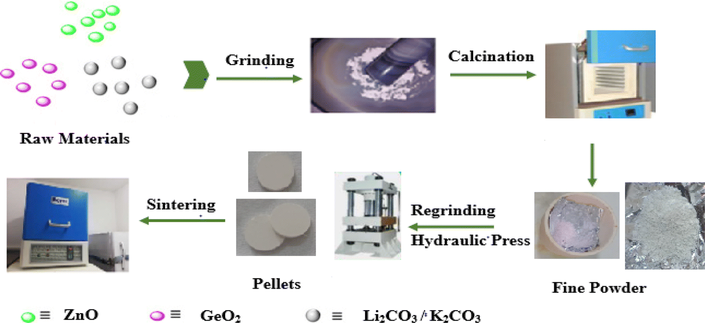


 and
and  ) and acceptors
  due to intrinsic defects in the host lattice at elevated temperatures.11
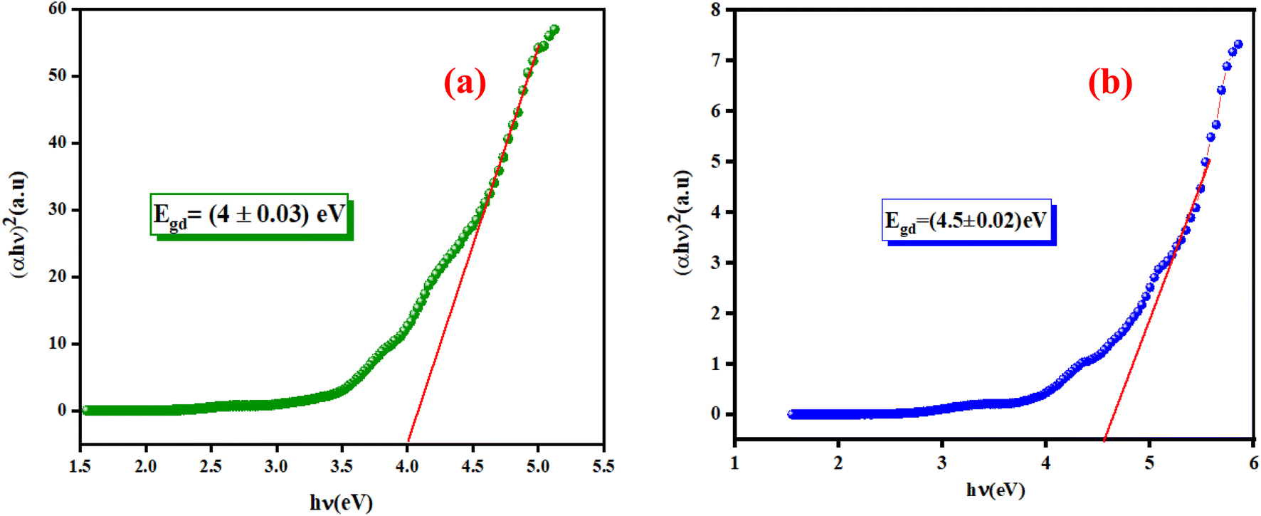


 and the static dielectric constant (εs) of the A2ZnGeO4 (A = K, Li) films were estimated using the presented relations:19,20
 and the static dielectric constant (εs) of the A2ZnGeO4 (A = K, Li) thin films. It is observed that by increasing the film thickness, the magnitudes of f, n0 and εs were raised. However, these factors are highly dependent on the refractive index measurements, which increase with increasing film thickness. Consequentially, the increased values of these factors (f, n0 and εs) are related to this rise in the refractive index values, and resulted from the enhancement of the crystallization of films, the movement of atoms towards other ones, and their organization in a more stacked manner, in addition to reduce the vacancies and crystal defects. According to the literature, similar findings have been reported for the dispersion parameters of other thin films.21,22 Along with these parameters, we have also calculated, utilizing the same model, the average oscillator wavelength (λ0) for the A2ZnGeO4 (A = K, Li) using the following equation:23


 , which is a consequence of the change in the refractive index linear, n0, due to the enhancement of crystallization and a reduction in the values of defects in crystals, stresses, and lattice strains that occur in the film materials. Comparable results for these nonlinear optical parameters were reported in earlier works involving similar thin films.35