
 Open Access Article
 This Open Access Article is licensed under a Creative Commons Attribution-Non Commercial 3.0 Unported Licence
Sb2S3/AlGaAs-based reconfigurable metasurface for dynamic polarization and directionality control of quantum emitter emission†
Md. Ehsanul Karim ab and
Sajid Muhaimin Choudhury*a
ab and
Sajid Muhaimin Choudhury*a
aDepartment of Electrical and Electronic Engineering, Bangladesh University of Engineering and Technology, Dhaka, 1205, Bangladesh. E-mail: sajid@eee.buet.ac.bd
bDepartment of Electrical and Electronic Engineering, BRAC University, Dhaka, 1212, Bangladesh
First published on 16th September 2024
Abstract
In this article, we report, to the best of our knowledge, for the first time, phase change material (PCM)-based reconfigurable metasurfaces for tailoring different degrees of freedom (DoF) of the quantum emitter (QE) emission, namely polarization and directionality, two key controlling factors in applications such as quantum computing, communication, and chiral optics. We have used a hybrid plasmon-QE coupled bullseye grating system utilizing the unexplored concept of composite nano-antennas in quantum photonics as the basic building block of the structures. Carefully engineered azimuthal width profile of the Sb2S3/AlGaAs composite ridge and selectively controlled transition of PCM (Sb2S3) states provide dynamic control over the amplitude and phase of the scattered radiation. Based on this methodology, we have designed five different metasurfaces for on-demand switching of target DoFs of QE emission, ensuring high collection efficiency due to the near-field coupling scheme. The first two metasurfaces switch the majority of the outgoing radiation from radially polarized to circularly polarized, whereas the next two switch the direction of circularly polarized outgoing radiation by a maximum of 9.23° while maintaining the spin state (or polarization chirality) in the simulation environment. The third metasurface category is capable of on-demand generation and separation of opposite spin states of outgoing radiation by 11.48° utilizing the selectively controlled phase transition of Sb2S3. Such reconfigurable multi-dimensional manipulation of QE radiation has not been investigated previously. This work proves the vast potential of active metasurfaces to modify the DoFs of QE emission, paving the way for high-dimensional quantum sources for high-speed quantum communication, higher dimensional quantum processing, and switchable chiral optics.
1 Introduction
Quantum emitters (QEs) are excited quantum dots, atoms, ions, or molecules acting as point-like light sources.1 They are one of the fundamental components of different quantum technologies such as quantum computation,2 quantum secure communication,3 and quantum-enhanced metrology.4 Ideally, these technologies require single photon sources with unity efficiency and radiation within a well-defined channel (in terms of frequency, direction, and polarization)5 and means to dynamically control these channel DoFs, producing the so-called high dimensional quantum sources.6 However, stand-alone quantum emitters are almost invariably characterized by their low emission rate, omnidirectionality, and poorly defined polarization state, hindering their direct integration in quantum technologies.7,8 Significant spontaneous emission rate enhancement has been achieved by coupling QEs to properly designed nano-structures due to the well-known Purcell effect.9,10 A high degree of directionality of QE radiation has been obtained through far-field reshaping of the radiated wavefront with lens and mirrors.11 Low collection efficiency is almost invariably encountered with this approach, which is solved by its near-field counterpart.12 Near-field coupling allows the efficient control of the far-field emission pattern through the non-radiative interaction of the surrounding nano-structure, namely bullseye gratings,13 Yagi–Uda antennas,14,15 nano-patch antenna,16 waveguides17 or hyperbolic metamaterials18 with the QE.In recent years, the variant of bullseye grating system composed of concentric dielectric circular ridges separated from a metal film by a dielectric spacer (also popularly known as hybrid QE-plasmon coupled metasurface) has attracted interest owing to their high quantum yield and collection efficiency.19 However, the symmetry of the structure limits the polarization state and directionality of outgoing waves to radial polarization and along the normal direction, respectively. Modern-day quantum technologies require precise control of these degrees of freedom (DoF) of the QE emission.20 To meet these requirements, different modifications of the bullseye array have been developed to control the polarization and chirality of the outgoing photons at room temperature.21–24 However, attaining the dynamic tuning of these DoFs of quantum emission through near-field coupling with nano-structures remains an issue.
The dynamic/active control of polarization and/or directionality of QE emission will boost bit rates in quantum communication, computational power, or dimensions of quantum computing systems and unlock new applications in the field of chiral quantum photonics,25–27 taking advantage of the resulting high-dimensional quantum source. There have been reports of dynamic polarization control of QE radiation using high-magnitude magnetic fields at cryogenic temperatures28 and spin-state splitting through far-field coupling with metalens.27,29 The latter category, however, suffers from low collection efficiency due to the randomness of spontaneous quantum emission and the far field coupling scheme and is not reconfigurable in nature, limiting its applications in quantum technologies.
Metasurfaces have significantly altered the global landscape of photonic design over the last few decades due to their distinct ability to independently control the phase and amplitude of the photons scattered from the constituent nano-antennas.30 This has led to the generation of electromagnetic waves with well-defined polarization, amplitude, and wavefront. The integration of the phase change material, graphene, PIN diode, varactor diode, liquid crystal, magnetic field-based switching and micro-electromechanical system (MEMS) as the switching mechanism with these meta-devices has led to the dynamic/active control of polarization, direction, and wavefront of the outgoing waves.31–39 Phase change materials (PCM), namely vanadium dioxide (VO2), Ge2Sb2Te5 (GST), antimony trisulfide (Sb2S3), Ge2Sb2Se4Te1 (GSST), due to their chemical and thermal stability, fast and repeatable switching, provide the most viable path for commercializing tunable metasurfaces.40 As a first stepping stone for integrating active metasurfaces in the quantum photonics realm, two recent reports have used PCM-based nano-structures to dynamically tune the Purcell enhancement.41,42 However, the inability of these works to produce on-demand switching of the polarization or direction, which are considered to be the basic DoFs of QE in quantum technology, means the true potential of tunable/active metasurfaces has not been explored adequately in the field of quantum photonics.43 To the best of our knowledge, reconfigurable active metasurface for tailoring direction and polarization of QE emission has not been reported to date.
In this work, we report PCM-based tunable bullseye grating metasurfaces for dynamic polarization and directionality control of QE emission. The composite ridge array of Sb2S3/AlGaAs is separated from the metallic layer by a dielectric, forming the hybrid QE-plasmon coupled bullseye metasurface. This structure combines the well-known azimuthally varying-width bullseye antenna used for controlling polarization of QE emission23 with the concept of composite nano-antennas used in phase gradient meta-surfaces.44,45 Such composite structures provide greater control over the phase of scattered light on each point of the device through the smart choice of individual material width profiles but have not been explored properly in the field of quantum photonics. The fast and repeatable switching of the PCM, Sb2S3, through electrical or optical excitation46,47 gives the meta-devices their tunability. Proper engineering of the phase and amplitude profile of the light scattered by the Sb2S3/AlGaAs composite ridge allowed the proposed metasurfaces to dynamically change the outgoing emission direction or polarization or both when the PCM phase transition occurs. Finite-difference time-domain (FDTD) simulations show an excellent collection efficiency of around 98% for all the metasurfaces due to the near-field coupling scheme of the hybrid QE-plasmon coupled metasurfaces. The first category of PCM-based metasurfaces (PMS), PMS-1R and PMS-1L, dynamically switches the outgoing photons from radially polarized (RP) to the right (RCP) and left (LCP) circularly polarized states, respectively, as Sb2S3 transitions from an amorphous to a crystalline state. The second and third classes of metasurfaces require the selective control of the PCM state in two quadrants of the bullseye grating. This allows the second metasurface generation proposed in this article (PMS-2) to dynamically deflect the outgoing circularly polarized waves while maintaining the same spin (circular polarization) state. The third class of metasurface, PMS-3, allows the on-demand switching of spin states accompanied by a spatial shift of 11.48° of outgoing photons utilizing selective transition of the Sb2S3 phase. Such reconfigurable multi-dimensional tailoring of QE radiation using metasurfaces has not been investigated in previous literature. The ability of our designed novel PCM-based bullseye grating structures to dynamically modify one or more DoFs of QE emission, along with the excellent collection efficiency, is expected to pave the way for further integration of active metasurfaces in the field of quantum photonics.
2 Structure layout
We have used the well-known bullseye configuration consisting of concentric circular nanoridges as the basic building block for our metasurfaces. The array of circular ridges is separated from the back metal layer (silver, Ag) by a dielectric (silicon dioxide, SiO2), forming the hybrid plasmon-QE coupled meta-device.48 A generalized representation of the phase change material (PCM)-based metasurfaces (PMS) used in this work is shown in Fig. 1. The Sb2S3/AlGaAs-based circular ridges in this figure have been drawn in a generalized way to summarize the different functionalities of the metasurfaces (dynamical switching of the directionality or polarization states or both of outgoing radiation). All the metasurfaces have been simulated using the finite-difference time-domain (FDTD) method in the commercial software Lumerical FDTD Solutions. Perfectly matched layer (PML) boundary conditions were used in all three directions. In the simulation environment, the quantum emitter (QE) is represented as a vertically oriented electric dipole placed at the center of the nanoridge array at a distance of 50 nm from the SiO2 top surface along the positive z-axis.21,23 We chose the wavelength for the dipole source to be 802 nm, which coincides with the zero-phonon line of the nickel–nitrogen complex (NE8) center of the diamond when pumped with 695 nm pulsed laser excitation at room temperature.49 For maximum emission intensity of the QE, the excitation source should be linearly polarized with polarization aligned with the dipole (z-axis) while propagating along either x or y direction in Fig. 1.50,51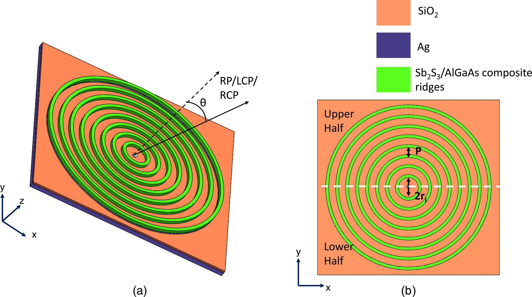 | ||
| Fig. 1 (a) Generalized 3D schematic representation of the PCM-based metasurfaces (PMS) composed of concentric circular nano-ridges with the quantum emitter at the center. The arrows represent the dynamic variation of scattered beam direction and polarization (radial (RP), right (RCP) or left (LCP) circularly polarized) with the Sb2S3 state. (b) x–y plane cross-sectional view of the designed metasurfaces, with the radius of the inner ridge (ri) and periodicity (P) of the nano-ridges marked. The Sb2S3/AlGaAs-based circular ridges here have been drawn in a generalized manner for all the metasurfaces considered and do not represent the exact construct used. The white dashed line divides the metasurface into two halves. Separate control over the PCM state is required in the individual halves for PMS-2 and 3. | ||
The QE (dipole source in FDTD simulations) couples radially diverging non-radiative surface plasmon polaritons (SPP) supported by the Ag–SiO2–air interface. The SPPs are scattered by the system of nano-ridges into outgoing free-propagating photons. The x–y plane cross-sectional view of a single ridge of the five metasurfaces is shown in Fig. 2. The number of nano-ridges in the bullseye grating controls the collection efficiency of outgoing radiation.52 Since a close to 98% collection efficiency is observed in this work for all structures with eight nano-ridges, this number has been kept constant throughout. All the structures utilize a hybrid ridge configuration combining Sb2S3 and AlxGa1−xAs layers with azimuthally varying widths. Careful design of the individual layer (AlGaAs and Sb2S3) widths and the composition (x) of AlxGa1−xAs allows us to dynamically control the directionality or polarization states or both the scattered beam as PCM state transition occurs, as schematically shown in Fig. 1(a). Sb2S3 was selected as the PCM due to its high refractive index and low absorption coefficient in both the amorphous and crystalline states at our desired frequency. The mole fraction of Al (x) in AlxGa1−xAs for PMS 1, 2, and 3 used in our calculations is 1, 0.7, and 0.7, respectively. The exact choice of the AlxGa1−xAs composition depends on the desired functionality of the respective PMS and will be discussed in detail in Sections 3.1, 3.2, and 3.3. The optical properties (complex relative permittivity) of the two states of Sb2S3, AlAs, and Al0.7Ga0.3As have been taken from previously reported results.53–55 The Palik model was used in our simulations for the relative permittivities of Ag and SiO2.56 The complex relative permittivities of all the materials input to the FDTD simulation environment are shown in Fig. S3 of the ESI.† The heights of Al and SiO2 have been kept constant at 50 nm and 200 nm, respectively, for all the five PMSs. We chose the values to ensure non-radiative SPP modes from the QE can be coupled to Al–SiO2–air, Al–SiO2–Sb2S3 (for both amorphous and crystalline states) and Al–SiO2–AlxGa1−xAs (x = 1, 0.7) stacks. The results and simulation setups for these calculations are shown in Fig. S1 of the ESI.† The other parameters, ri and the height of the ridge array (h), have been chosen to engineer the scattering phase and amplitude to achieve the desired directionality and polarization state of the outgoing photons. The calculation of P is based on effective medium theory. The detailed calculations can be found in Section 1 of the ESI.†
 | ||
| Fig. 2 (a) x–y plane cross-section view of a single circular ridge of the bulls-eye array and (b) x–z plane cross-sectional view of the PMS-1 metasurface. x–y plane cross-section view of a single circular ridge of the bulls-eye array for (c) PMS-1L, (d) PMS-2R, (e) PMS-2L, and (f) PMS-3. The insets in (c)–(f) represent the x–z cross-sections of the respective circular ridges. The dashed lines through the center in (d)–(f) represent the two halves of the metasurface (in Fig. 1(b)) in which selective control over the PCM state is required. The thicknesses of Ag and SiO2 layers are 200 nm and 50 nm for all five structures. The thickness of the ridges (h) for PMS-1R and PMS-1L is 140 nm and for PMS-2L, PMS-2R, and PMS-3 is 150 nm. The total width of the ridge (w2) in (a) and (b) for PMS-1R and PMS-1L is 250 nm. The Sb2S3 width (w1) varies from 0 to 250 nm and from 250 to 0 nm with azimuthal angle (θ) variation of 0 to 2π radian for PMS-1R and PMS-1L, respectively. w1 is varied from 0 to 85 nm and 85 nm to 0 for PMS-2R and PMS-2L in (d) and (e), respectively, over the complete range of θ. The width of AlGaAs (w3) is kept constant at 200 nm for both structures. For PMS-3 in (f), w2 is 240 nm and w1 is varied from 0 to 100 nm for θ = 0 to π radian and 100 nm to 0 for θ = π to 2π radian. | ||
The metasurface structure PMS-1R(L) (Fig. 2(a) and (b)) dynamically switches the polarization state of the emitted photons from radial polarization (RP) to the right (left) hand circular polarization when Sb2S3 transitions from an amorphous (AA state of the metasurface) to a crystalline (CC state) phase. The third metasurface proposed in this work, PMS-2R, schematically shown in Fig. 2(c), generates an RCP beam with the Sb2S3 in the upper and lower half of the metasurface in the amorphous and crystalline phase, respectively (AC state of the metasurface) (or vice versa (CA state)). When the metasurface transitions from AC to CA (or CA to AC), the outgoing beam gets deflected, maintaining the same polarization state (RCP). The PMS-2L structure dynamically deflects LCP radiation when switched between AC and CA states. PMS-3 allows the dynamic switching of outgoing photon polarization from RCP to LCP when reconfigured from CA to the AC state. This polarization transition is accompanied by a deflection of the peak intensity position, manifesting reconfigurable multifunctionality.
Circular nano-ridges with azimuthally varying widths on SiO2/Ag have been fabricated in several previous literature reports.22,23,57 These works also report excellent fabrication tolerance of such structures in controlling QE emission. The Ag substrate can be deposited using ohmic evaporation on a Silicon wafer. The SiO2 layer can be fabricated using RF sputtering. Further details about the alignment of the ridge patterns and the quantum dot can be found in ref. 23. Growth of AlGaAs for x = 0.7 and 1 can be done using liquid phase epitaxy and organometallic chemical vapor deposition, respectively.55 Deposition of Sb2S3 on a thin SiO2 layer has also been investigated in previous reports.58 These works prove the feasibility of our proposed PMS structures. However, the hands-on implementation of the devices is beyond the scope of this work. The Sb2S3 layers can be switched reversibly between amorphous and crystalline states using a laser diode operating at 638 nm wavelength and capable of producing variable optical pulse durations.53 Moreover, control over the Sb2S3 switching region can be exercised by changing the laser pulse duration or power. Such laser-based phase transition methodology of PCMs has been integrated into different nano-structures as reported previously.59,60 Selective control of the PCM state in meta-devices with nanometer resolution has been investigated in previous literature.61,62 These reports prove the feasibility of our methodology requiring individual PCM states in the upper and lower halves of the metasurfaces.
3 Results and discussions
3.1 Switching between radial and circular polarization
Our proposed PMS-1R and 1L structures dynamically switch the outgoing photons from radially polarized to right and left circularly polarized states, respectively. This is achieved when the Sb2S3 in both halves of the metasurfaces switch from the amorphous (state AA) to the crystalline (state CC) phase through optical excitation. Both the polarization states are extremely important in the field of quantum photonics. RP photons with longitudinally polarized fields find applications in several quantum technologies such as quantum key distributions and quantum communication63,64 while circular polarization chirality represents the spin state of photons29 and finds applications in chiral quantum photonics.65The design methodology of PMS-1R is depicted in Fig. 3. The heights of Ag and SiO2 layers are 200 nm and 50 nm, respectively, as described in Section 1 of the ESI.† The parameters, h, w2, and ri, were recursively tuned to best match the required scattering phase angles (φ). Each time, the period (P) is updated using the effective medium theory (see ESI† for detailed calculations). The phase calculations were done numerically using the 2D simulation setup shown in Fig. 3(a). The final values chosen for these parameters are ri = 515 nm, w2 = 250 nm, h = 140 nm, and P = 475 nm. Scattering radially polarized waves requires the electric field scattered from each point on the metasurface to have the same phase.19 For this, we have chosen AlAs as the second material, which has almost the same refractive index as amorphous Sb2S3 at 802 nm. So, azimuthally increasing the Sb2S3 width (w1) will keep the effective index almost constant for the AA state. This produces an azimuthally constant phase of the scattered electric field (φ), as illustrated in Fig. 3(c). Other mole fraction values of AlGaAs produce a varying phase with changing Sb2S3 width due to the mismatch in refractive index, making them unsuitable for producing radial polarization in the AA state (see Fig. S4 of the ESI†). For Sb2S3 in the crystalline state, φ increases with w1 due to the increase in effective refractive index. As w1 varies from 0 to 250 nm, φ also achieves a 2π phase coverage for crystalline Sb2S3 (Fig. 3(d)). So, linearly varying w1 with azimuthal angle (θ) ensures that electric fields scattered from any two points on the ridge displaced in θ by π/2 are not only orthogonal but also out of phase by π/2 in the CC state. This will produce outgoing right circularly polarized waves in the far-field pattern for this state. For PMS-1R(L), w1 is increased (decreased) (Fig. 2(a) and (b)) linearly to achieve the required spatial variation of φ to produce RCP (LCP) photons in the CC state.57
 | ||
| Fig. 3 Design procedure of PMS-1R. (a) 2D FDTD simulation setup for calculating the variation of the phase of scattered light (φ) with Sb2S3 width (w1). The position of the monitor is also marked. w1 was varied between 0 and 250 nm, keeping w2 constant at 250 nm. (b) x–y plane cross-section of a single circular ridge of PMS-1R. Required and realized relative phase values for variation of w1 for (c) AA and (d) CC states of the metasurface. For these simulations, the heights of Ag, SiO2, and ridge (h) have been kept constant at 200 nm, 50 nm, and 140 nm, respectively. The values for the inner radius (ri) and the total ridge width (w2) are 515 nm and 250 nm, respectively. | ||
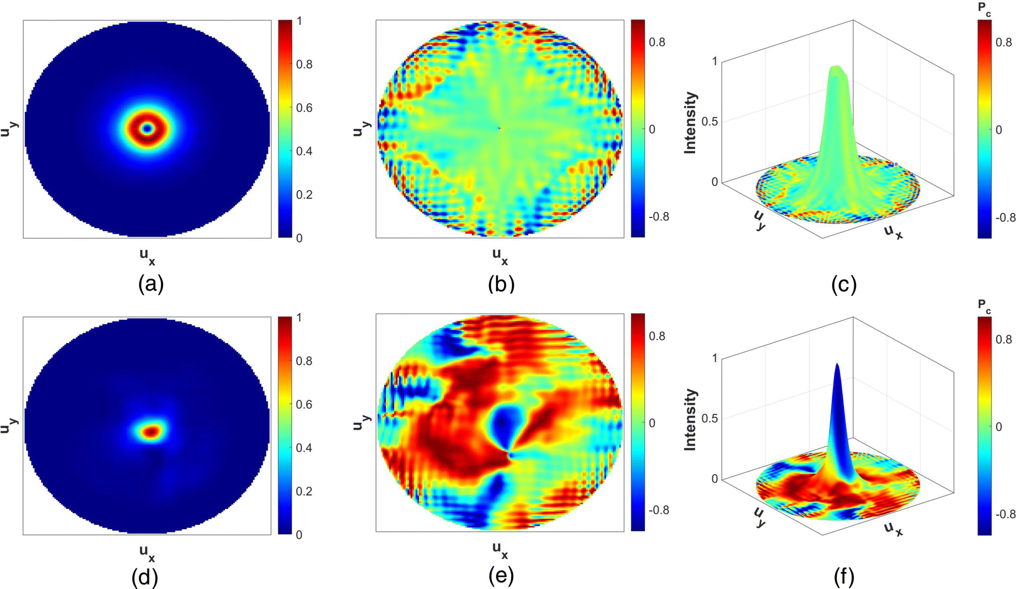
The optical properties of PMS-1R and 1L have been evaluated using 3D FDTD simulations with the simulation settings described in Section 2. The far-field intensity and polarization states of the scattered free-propagating waves for CC and AA states are shown in Fig. 4 and 5, respectively. The coordinates in far-field patterns, ux and uy, have been used to show a flattened data curve, with the point (0, 0) representing scattering along the normal direction. Further details about this coordinate system can be found in Section 6 of the ESI.† To evaluate the polarization state, we have used the normalized Stokes parameter (Pc). This is used as a measure of the degree and chirality of circular polarization in the far-field pattern. The values −1, 0, +1 of Pc denote pure LCP, linearly polarized, and RCP states. However, in the context of circular ridges, the value 0 represents radial polarization.57 The detailed equations for calculating Pc can be found in Section 2 of the ESI.†
 | ||
| Fig. 4 Far-field optical characteristics of PMS-1R for the (a)–(c) AA and (d)–(f) CC states calculated from 3D FDTD simulations. (a) and (d) represent far-field intensity distributions for AA and CC states, respectively. (b) and (e) depict the far-field polarization state distributions of PMS-1R with AA and CC states, respectively. The red, blue, and green colors correspond to right circular, left circular and radial polarizations, respectively. (c) and (f) Illustrate the superimposed 3d representation of the beam intensity and polarization distributions, with the height and color indicating the intensity and polarization of the outgoing photons, respectively. All the intensity values have been normalized by their respective maxima. In all the simulations, the standard configuration of the QE described in Section 2 with an emission wavelength of 802 nm was used. | ||
 | ||
| Fig. 5 Far-field optical characteristics of PMS-1L for the (a)–(c) AA and (d)–(f) CC states calculated from 3D FDTD simulations. (a) and (d) represent far-field intensity distribution for AA and CC states, respectively. (b) and (e) depict the far-field polarization state distributions of PMS-1L with AA and CC states, respectively. The red, blue, and green colors correspond to right circular, left circular and radial polarizations, respectively. (c) and (f) Illustrate the superimposed 3d representation of the beam intensity and polarization distributions, with the height and color indicating the intensity and polarization of the outgoing photons, respectively. All the intensity values have been normalized by their respective maxima. In all the simulations, the standard configuration of the QE described in Section 2 with an emission wavelength of 802 nm was used. | ||
For the PMS-1R structure in the AA state, the far-field intensity distribution shows a collimated doughnut-shaped pattern at the center (Fig. 4(a)). The distributions of Pc show that the majority of the outgoing photons are radially polarized for this state (Fig. 4(b)), quantified by Pc = 0. In the CC state, a bright spot around the center of the far-field distribution is observed for PMS-1R (Fig. 4(d)). The distribution of the normalized Stokes parameter (Pc) for PMS-1R in Fig. 4(e) has a red spot with Pc > 0.8 (RCP) coinciding with the maximum intensity location. Some of the photons are indeed emitted with opposite chirality (LCP) as found in the previous relevant literature as well.57 However, the chirality-intensity superimposed distribution in Fig. 4(f) shows that the majority of the outgoing radiation is right circularly polarized. So, PMS-1R can dynamically change a majority of the scattered photons from RP to RCP when switched from AA to the CC state.
PMS-1L also shows very similar far-field characteristics. A similar radially polarized doughnut pattern is observed for this structure as well in the AA state (Fig. 5(a)–(c)). The majority of the out-coupled radiation dynamically switches to LCP when Sb2S3 transitions to its crystalline state (CC state). This is represented by the blue region in the Pc distribution (Fig. 5(e)) coinciding with the maximum intensity location as illustrated in Fig. 5(f).
As a measure of directionality, we have calculated the collection efficiency (CE) of both the PMS-1 variants. This quantity is defined as the fraction of out-coupled power collected by the first objective with a numerical aperture of 0.9 (within a 64° cone).19 We have also calculated the full width at half maximum (FWHM) of the intensity distribution. Another important parameter for evaluating nano-structures coupled to QE is the Purcell Factor (PF). This quantity is defined as the ratio of the power emitted by the QE with and without the bullseye grating environment. These values for both the structures in CC and AA states are summarized in Table 1. The performance parameters for both structures are almost identical in both AA and CC states. CE is around 98% in both the structures for either state. FWHM is relatively higher for the CC state compared to previous works. This can be attributed to the high refractive index of the circular ridges used in this work compared to the former. Similar observations have been made in previous literature as well.57 Also, for both structures, FWHM is relatively higher in the AA state. This is due to the doughnut pattern of the radially polarized wave. The high FWHM value is, however, consistent with previously reported values for RP patterns.19
| Structure | State | CE (%) | PF | Peak position | FWHM | Polarization |
|---|---|---|---|---|---|---|
| PMS-1R | AA | 97.78 | 1.63 | 5.88° | 9.9° | RP |
| CC | 98.33 | 2.01 | 4.07° | 7.6° | RCP | |
| PMS-1L | AA | 97.66 | 1.75 | 5.88° | 10.04° | RP |
| CC | 98.31 | 2.05 | 4.07° | 7.64° | LCP |
3.2 Dynamic deflection of circular polarized outgoing waves
The PMS-2R(L) metasurface scatters SPP coupled in the Ag/SiO2 interface into right (left) circularly polarized outgoing photons. As the structure switches between AC to CA states, the scattered beam gets deflected, maintaining its respective chirality (RCP for PMS-2R and LCP for PMS-2L). Such spatial multiplexing of outgoing radiation while maintaining the spin state is expected to contribute greatly to high-power quantum processing technologies.21,25The design procedure for the PMS-2R structure has been depicted in Fig. 6. Since we desire the metasurface to produce RCP beams for both the AC and CA states, we require both the amorphous and crystalline states to produce similar values of the scattered electric field phase (φ) for different w1. For this, we iteratively tuned different structural parameters (h, w3, ri, x) to match the phase requirements. SiO2 and Ag heights have been maintained at 50 nm and 200 nm, respectively, during the entire procedure. The value of P is updated each time based on the effective medium theory described in Section 1 of the ESI.† The simulation setup used for phase calculation is the same as the one described in Fig. 3(a). The best possible matching of φ for the two states of Sb2S3 is achieved for h = 150 nm, P = 500 nm, ri = 515 nm, w3 = 200 nm, and x = 0.7. Further details about the choice of the Al-GaAs stoichiometry (x) can be found in Fig. S5 of the ESI.† The variation of φ with w1 for this configuration is shown in Fig. 6(b) for the amorphous and crystalline states of Sb2S3. As w1 is varied from 0 to 85 nm, the relative value of φ covers a 7.3 radian range for the crystalline state and 5.33 radian for the amorphous state.
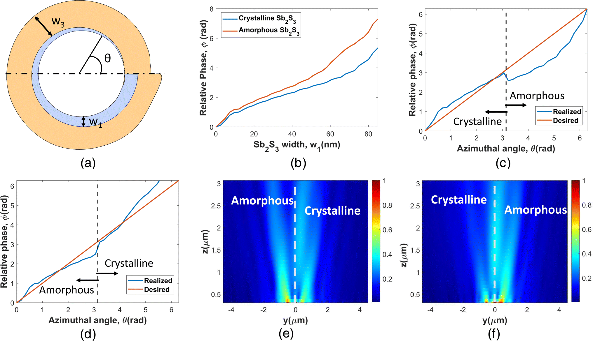 | ||
| Fig. 6 Design procedure of PMS-2R. (a) x–y plane cross-section of a single circular ridge of PMS-2R. (b) Variation of the scattered light phase (φ) with Sb2S3 (in crystalline and amorphous states) width (w1) for a constant Al0.7Ga0.3As width (w3) of 200 nm. Required and realized relative phase values at azimuthal position θ for the (c) CA and (d) AC state of the PMS-2R metasurface. y–z plane distribution of the electric field magnitude of PMS-2R at (e) CA and (f) AC states. For this simulation, the 2d monitor was placed along the y-axis through the metasurface center. The field magnitudes have been normalized by their respective maxima. | ||
This range of w1 gives the best possible match between the two. Though the absolute value of the difference in φ for amorphous and crystalline Sb2S3 increases gradually with increasing w1, as seen in Fig. 6(a), and the relative error remains almost static.
For the AC and CA states of PMS-2R, the realized and desired values of φ are shown in Fig. 6(b) and (c), respectively. Producing RCP outgoing waves requires the phase of the scattered electric field (φ) at any point on the ridge to increase linearly with azimuthal position (θ), as explained in Section 3.1. The realized profiles of φ for the two states do not exactly match the requirements but are very close to the latter. For dynamically deflecting the RCP beam, the structure needs to be switched from AC to the CA state or vice versa. In the CA state, for example, the upper half of the metasurface in the x–y plane has a higher refractive index (crystalline Sb2S3) than the lower half (amorphous Sb2S3). It is well-known that high refractive index materials produce higher scattering.57 This is further validated by the scattering cross-sections of an Sb2S3 nano-cube in the amorphous and crystalline states, shown in Fig. S7 of the ESI.† The results show that the crystalline Sb2S3 with a higher refractive index at our target wavelength of 802 nm has a higher scattering cross-section. As a result, the beam gets deflected towards the lower half of the metasurface in the x–y plane (or equivalently towards the left half in the y–z plane, as shown in Fig. 6(e)). For the AC state, the beam gets deflected towards the right half of the metasurface in the y–z plane, as illustrated in Fig. 6(f). Since in both the states, the respective phase requirements for RCP beam generation are also roughly met, we expect the beam to get deflected, maintaining the same polarization.
We have numerically studied the optical characteristics of the PMS-2R structure in the AC and CA states using the 3D FDTD simulation method. The 3D superimposed representation of the far-field normalized Stokes parameter (Pc) and intensity distributions show that the locations of maximum intensity coincide with that of the red-colored region corresponding to RCP radiation (Pc > 0.8) for both the states (Fig. 7(b) and (d)). The relative shifting of the intensity distributions is also visible in the far-field pattern (Fig. 7(a) and (c)). The shifting between the peak positions is 9.23°, evident in the cross-sectional intensity distributions in Fig. 7(e).
 | ||
| Fig. 7 Far-field optical characteristics of PMS-2R for the (a)–(b) and (c)–(d) AC states calculated from 3D FDTD simulations. (a) and (c) represent far-field intensity distribution for CA and AC states, respectively. Superimposed 3d representation of the beam intensity and polarization distributions for (b) CA and (d) AC states, with the height and color indicating the intensity and polarization of the outgoing photons, respectively. The red, blue, and green colors denote right circular, left circular and radial polarizations, respectively. (e) Normalized cross-sectional intensity profiles (along the white dashed lines) for CA and AC states. All the intensity values have been normalized by their respective maxima. In all the simulations, the standard configuration of the QE described in Section 2 with an emission wavelength of 802 nm was used. | ||
Table 2 summarizes different performance parameters of the PMS-2R structure in both the CA and AC states. The collection efficiency (CE) is high like other proposed structures; however, FWHM is relatively higher. For the CA state, there is a side lobe appearing close to the maxima with the opposite chirality (Fig. 7(b)). This feature has been found in previous relevant works as well.57 Also, the intensity distribution of the outgoing radiation in the AC state appears to be smeared (Fig. 7(c)). Both these features of the intensity distribution can be attributed to the mismatch between realized and desired profiles of φ.57 Also, PF is approximately the same for both states.
| Structure | State | CE (%) | PF | Peak position | FWHM | Polarization |
|---|---|---|---|---|---|---|
| PMS-2R | CA | 98.9 | 1.9 | −4.26° | 10.86° | RCP |
| AC | 98.87 | 2 | 4.97° | 10.6° | RCP | |
| PMS-2L | CA | 98.63 | 1.79 | −3.56° | 11.68° | LCP |
| AC | 98.95 | 1.84 | 4.48° | 10.82° | LCP |
The methodology for designing metasurface (PMS-2L) to dynamically deflect the outgoing LCP radiation is similar to that for PMS-2R described in Fig. 6. For the PMS-2L structure, w1 is linearly decreased from 85 nm to 0 nm with increasing azimuthal angle (θ) (as schematically shown in Fig. 2(d)), to produce LCP light in both the AC and CA states. Other structural parameters are the same as PMS-2R. The superimposed representations of polarization and intensity for the two states (Fig. 8(b) and (d)) further verify that the majority of outgoing radiation is left circularly polarized. As the structure is switched from AC to CA (or vice versa), the peak position undergoes an angular displacement of 8.04°, as can be seen in the intensity cross-sections for the two states (Fig. 8(e)). The intensity distributions for the AC and CA states of PMS-2L (Fig. 8(a) and (c)) are also similar to that of the PMS-2R structure. A smeared peak for the CA state and a side lobe for the AC state are also evident in the far-field intensity profiles. This results in a relatively high FWHM for this meta-device, as observed for the PMS-2R structure. Different performance parameters of the PMS-2R structure, namely FWHM, CE, and PF, are summarized in Table 2.
 | ||
| Fig. 8 Far-field optical characteristics of PMS-2L for the (a)–(b) CA and (c)–(d) AC states calculated from 3D FDTD simulations. (a) and (c) represent far-field intensity distribution for CA and AC states, respectively. Superimposed 3d representation of the beam intensity and polarization distributions for (b) CA and (d) AC states, with the height and color indicating the intensity and polarization of the outgoing photons, respectively. The red, blue, and green colors denote right circular, left circular and radial polarizations, respectively. (e) Normalized cross-sectional intensity profiles (along the white dashed lines) for CA and AC states. All the intensity values have been normalized by their respective maxima. In all the simulations, the standard configuration of the QE described in Section 2 with an emission wavelength of 802 nm was used. | ||
3.3 Simultaneous circular polarization and direction switching
Our final proposed metasurface, PMS-3, is capable of simultaneously switching the chirality (or spin angular momentum) and direction of circular polarized outgoing radiation when it transitions from AC to the CA state through selective optical excitation of Sb2S3. The design methodology for this metasurface is shown in Fig. 9. In terms of polarization, we require scattering the SPP coupled from excited QE into RCP and LCP radiation for CA and AC states, respectively. For this, the phase of the scattered electric field (φ) should linearly increase and decrease respectively with azimuthal angle (θ). This readily poses the need for a contrasting trend of φ with increasing w1 for crystalline and amorphous phases of Sb2S3.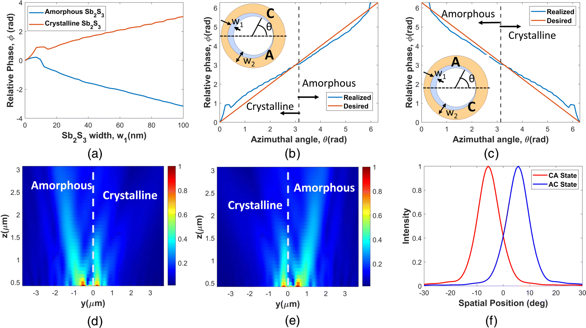 | ||
| Fig. 9 Design procedure of PMS-3. (a) Variation of the scattered light phase (φ) with Sb2S3 (in crystalline and amorphous states) width (w1) for a constant total width (w2) of 240 nm. Required and realized relative phase values at azimuthal position θ for the (b) CA and (c) AC states of the PMS-3 metasurface. The insets show the x–y plane cross-section of a single circular ridge, with different parameters marked and the Sb2S3 phase of each half. y–z plane distribution of the electric field magnitude of PMS-3 at (d) CA and (e) AC states. For this simulation, the 2d monitor was placed along the y-axis through the metasurface center. (f) Normalized cross-sectional intensity profiles (along the white dashed lines in Fig. 10(a) and (d)) for CA and AC states. The field magnitudes have been normalized by their respective maxima. | ||
The phase profile calculation was done numerically using the same 2d simulation setup in Lumerical FDTD Solutions as described in Fig. 3(a), with a constant total width (w2). We have chosen Al0.7Ga0.3As as the second material, which has a refractive index value roughly right in between the two Sb2S3 phases at 802 nm wavelength. As Sb2S3 width (w1) increases, the width of AlGaAs decreases. As amorphous Sb2S3 has a lower refractive index than Al0.7Ga0.3As, increasing w1 decreases the effective index of the ridge, resulting in a decrease in φ (Fig. 9(a)). Conversely, for crystalline Sb2S3, φ increases with w1. The fact that Al0.7Ga0.3As has a refractive index between the two states of Sb2S3, the increase in w1 produces approximately equal and opposite changes in the relative phase values for the two states (Fig. 9(a)). This ensures that RCP and LCP light can be scattered in the CA and AC states of the PMS-3 structure, respectively. Other molar fractions (x) of AlGaAs do not produce such equal and opposite spatial phase profiles for the two states, as shown in Fig. S6 of the ESI.† However, we found that achieving the complete 2π phase coverage for either of the states with a constant h is difficult. So, we modified the metasurface cross-section with w1 increasing linearly for the azimuthal position, θ = 0 to π radian and then decreasing linearly for π to 2π, as illustrated in Fig. 2(e). This effectively reduces the phase coverage requirement for both the Sb2S3 phases to π.
The variation of φ for increasing w1 with h = 150 nm, ri = 515 nm, w2 = 240 nm, and P = 400 nm for amorphous and crystalline Sb2S3 is depicted in Fig. 9(a). For w1 ranging from 0 to 100 nm, φ linearly increases (decreases) from 0 to π (−π) for crystalline (amorphous) Sb2S3. As a result, the azimuthal phase requirements for both the CA and AC states of the PMS-3 structure are almost perfectly matched, as can be seen in Fig. 9(b) and (c), respectively.
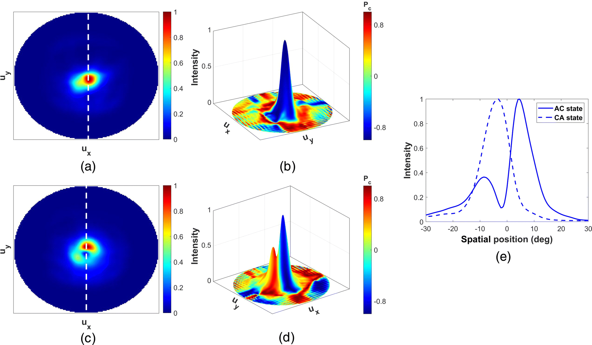
We have also simulated the y–z plane electric field profile of the PMS-3 structure for both the AC and CA states (Fig. 9(d) and (e)). The outgoing beam gets scattered towards the left half of the y–z plane due to the high scattering from the crystalline Sb2S3 present in the right half. For the AC state, the opposite condition occurs. This deflection is also evident in the far-field intensity distributions in Fig. 10(a) and (d) and also in the cross-sectional intensity distributions in Fig. 9(f). The cross-sectional intensities were taken along the white dashed lines shown in the respective far-field patterns. The positions of the intensity peaks suffer a relative shift of 11.483°. Other performance parameters of the intensity distribution are also summarized in Table 3. We have been able to achieve very high CE values for both states, as with the previous structures. Also, FWHM is lower than PMS-2R and 2L structures. This can be attributed to the better matching of φ to the requirements. Also, the intensity distributions are almost symmetric concerning each other, apart from the deflection. This is evident in the intensity cross-sections depicted in Fig. 9(f). This is because of the symmetry of the Sb2S3 profile about the y-axis, as described previously. Also, the PF for this metasurface is lower than the previously discussed structures. This may be attributed to the fact that the choice of ri is dependent on the phase requirements, rather than matching the peak position of scattered intensity with the NE8 center emission wavelength (Fig. S2 of the ESI†). A detailed explanation of this can be found in Section 1 of the ESI.†
 | ||
| Fig. 10 Far-field optical characteristics of PMS-3 for the (a)–(c) CA and (d)–(f) AC states from 3D FDTD simulations. (a) and (d) represent far-field intensity distributions for CA and AC states, respectively. (b) and (e) depict the far-field polarization state distributions of PMS-3 with CA and AC states, respectively. The red, blue, and green colors correspond to right circular, left circular and radial polarizations, respectively. (c) and (f) Illustrate the superimposed 3d representation of the beam intensity and polarization distributions, with the height and color indicating the intensity and polarization of the outgoing photons, respectively. All the intensity values have been normalized by their respective maxima. In all the simulations, the standard configuration of the QE described in Section 2 with an emission wavelength of 802 nm was used. | ||
| Structure | State | CE (%) | PF | Peak position | FWHM | Polarization |
|---|---|---|---|---|---|---|
| PMS-3 | CA | 98.27 | 1.2 | −5.74° | 9.8° | RCP |
| AC | 98.20 | 1.24 | 5.743° | 9.8° | LCP |
We have also investigated the polarization state of the outgoing photons in terms of the normalized Stokes parameter (Pc). The red (blue) region in the far-field distribution of Pc (Fig. 10(b) and (e)) coincides with the location of the intensity distribution peak for the CA (AC) state. This means that the majority of the scattered photons are RCP and LCP polarized, respectively, for the CA and AC states. This is further verified in the intensity-Pc superimposed distributions for the two states in Fig. 10(c) and (f), respectively. So, by exerting control over the Sb2S3 phase in two halves of the metasurface, direction and circular polarization chirality can be simultaneously switched, manifesting switchable multifunctionality. This is the first report of QE integrated reconfigurable multifunctional metasurface. Such multi-dimensional switching of QE radiation will find significant applications in the transition of quantum computing towards higher dimensions.
Another issue regarding the three latter structures (PMS-2R, PMS-2L, and PMS-3) worth mentioning is the requirement of selective phase switching of the Sb2S3 ridges. In the simulations, we have assumed that the selection is perfect; that is, either half can be switched without affecting the other. However, such an abrupt phase boundary may not be possible in practice, where we expect a transition region with intermediate states to appear. This will result in a discrepancy between the simulation and experimental results. Having said that, the ever-improving resolution of laser switching methods for PCM switching59 will ensure the transition region is small enough. Moreover, based on the fabrication tolerance studies of such circular ridge structures,57 we believe that the basic operations of the three meta-devices can still be realized in practice despite some discrepancies.
Table 4 compares the PCM-based metasurfaces proposed in this work with previously reported tunable QE systems. It shows that there has been no previous report on the dynamic tailoring of QE emission direction or polarization utilizing reconfigurable nanostructures. Previous reports of direction switching for different spin states27,29 are based on far-field coupling with polarization switched metalens. The use of a far-field coupling scheme, along with the fact that spontaneous emission from QE is randomly polarized and results in low CE for both works. In addition to this, the meta-devices used are not reconfigurable in nature, reiterating the novelty of our work. The reconfigurable nano-device-based works41,42 have mainly focused on PF tuning, leaving out the more important DoFs of the QEs. The novel methodology of on-demand switching of direction and polarization of QEs proposed in this work combining Sb2S3 phase transition and the concept of composite nano-antennas is expected to lead to high-performing systems in the fields of next-generation quantum computing, chiral optics and communication.
| Switching mechanism | Switched/tuned parameter | Coupling scheme | CE | Reference |
|---|---|---|---|---|
| PCM (Sb2S3, VO2, graphene for different wavelengths) | PF | Near-field | — | 41 |
| Electro-optic (lithium niobite) | PF | Near-field | — | 42 |
| Wavelength switched micro-cavity | PF | Near-field | 93.2% | 66 |
| Polarization switched metalens | Spin-state splitting | Far-field | 30% | 27 |
| Polarization switched metalens | Spin-state splitting | Far-field | 32% | 29 |
| PCM (Sb2S3) | Polarization (PMS-1) | Near-field | 97.66% (minimum) | This work |
| Direction (PMS-2) | 98.63% (minimum) | |||
| Direction and polarization (PMS-3) | 98.20% (minimum) |
4 Conclusion
In this article, we propose PCM-based hybrid QE-plasmon coupled metasurfaces for dynamic control of polarization and directionality of QE emission. Such on-demand tailoring of QE emission parameters is reported for the first time in this work. Carefully engineered azimuthal width profile of Sb2S3/AlGaAs composite ridges and selectively controlled switching of the PCM phase allows the reported devices to exert dynamic control over different degrees of freedom of the scattered emission. We have numerically investigated five different metasurfaces for the active control of one or more DoFs of the emitted photons. All the structures demonstrate an excellent collection efficiency of around 98% due to the near-field coupling scheme of the bullseye grating. The first category of metasurfaces, PMS-1R and PMS-1L, switch the polarization state of the majority of photons from radially polarized to right and left circularly polarized, respectively. PMS-2R and PMS-2L produce dynamic switching of the beam position while maintaining the circular polarization chirality. The peak position experiences a shift of 9.23° and 8.04°, respectively, for the two structures. The final metasurface, PMS-3, produces spatially separated beams with opposite spin states of the majority of outgoing photons for two different states of the PCM. Such on-demand spatial switching for opposite circular polarization has not been investigated in previous reports. The findings of this work are expected to pave the way for tunable high-dimensional quantum sources utilizing active metasurfaces leading to high-speed quantum communication, higher dimensional quantum processing, and switchable chiral optics.Data availability
The datasets used and analyzed during the current study are available from the corresponding author upon reasonable request.Conflicts of interest
There are no conflicts to declare.Notes and references
- W. L. Barnes, S. A. Horsley and W. L. Vos, J. Opt., 2020, 22, 073501 CrossRef CAS.
- F. Shah, T. L. Patti, O. Rubies-Bigorda and S. F. Yelin, Phys. Rev. A, 2024, 109, 012613 CrossRef CAS.
- D. A. Vajner, L. Rickert, T. Gao, K. Kaymazlar and T. Heindel, Adv. Quantum Technol., 2022, 5, 2100116 CrossRef.
- V. Paulisch, M. Perarnau-Llobet, A. González-Tudela and J. I. Cirac, Phys. Rev. A, 2019, 99, 043807 CrossRef CAS.
- A. F. Koenderink, ACS Photonics, 2017, 4, 710–722 CrossRef CAS PubMed.
- J. Liu, M. Shi, Z. Chen, S. Wang, Z. Wang and S. Zhu, Opto-Electron. Adv., 2021, 4, 200092 Search PubMed.
- A. G. Curto, G. Volpe, T. H. Taminiau, M. P. Kreuzer, R. Quidant and N. F. Van Hulst, Science, 2010, 329, 930–933 CrossRef CAS PubMed.
- I. Aharonovich, D. Englund and M. Toth, Nat. Photonics, 2016, 10, 631–641 CrossRef CAS.
- A. Krasnok, S. Glybovski, M. Petrov, S. Makarov, R. Savelev, P. Belov, C. Simovski and Y. Kivshar, Appl. Phys. Lett., 2016, 108, 211105 CrossRef.
- A. Chebykin, V. Babicheva, I. Iorsh, A. Orlov, P. Belov and S. Zhukovsky, Phys. Rev. A, 2016, 93, 033855 CrossRef.
- S. Morozov, S. Vezzoli, A. H. Khan, I. Moreels and R. Sapienza, APL Photonics, 2020, 5, 071302 CrossRef CAS.
- J. Hadden, J. Harrison, A. C. Stanley-Clarke, L. Marseglia, Y.-L. Ho, B. Patton, J. L. O’Brien and J. Rarity, Appl. Phys. Lett., 2010, 97, 241901 CrossRef.
- R. Hekmati, J. P. Hadden, A. Mathew, S. G. Bishop, S. A. Lynch and A. J. Bennett, Sci. Rep., 2023, 13, 5316 CrossRef CAS PubMed.
- T. H. Taminiau, F. D. Stefani and N. F. van Hulst, Opt. Express, 2008, 16, 10858–10866 CrossRef PubMed.
- J. Kim, Y.-G. Roh, S. Cheon, J.-H. Choe, J. Lee, J. Lee, H. Jeong, U. J. Kim, Y. Park and I. Y. Song, et al., Nano Lett., 2014, 14, 3072–3078 CrossRef CAS PubMed.
- G. M. Akselrod, C. Argyropoulos, T. B. Hoang, C. Ciracì, C. Fang, J. Huang, D. R. Smith and M. H. Mikkelsen, Nat. Photonics, 2014, 8, 835–840 CrossRef CAS.
- M. Arcari, I. Söllner, A. Javadi, S. L. Hansen, S. Mahmoodian, J. Liu, H. Thyrrestrup, E. H. Lee, J. D. Song and S. Stobbe, et al., Phys. Rev. Lett., 2014, 113, 093603 CrossRef CAS PubMed.
- A. Davoyan and H. Atwater, Optica, 2018, 5, 608–611 CrossRef CAS.
- S. K. Andersen, S. Bogdanov, O. Makarova, Y. Xuan, M. Y. Shalaginov, A. Boltasseva, S. I. Bozhevolnyi and V. M. Shalaev, ACS Photonics, 2018, 5, 692–698 CrossRef CAS.
- A. S. Solntsev, G. S. Agarwal and Y. S. Kivshar, Nat. Photonics, 2021, 15, 327–336 CrossRef CAS.
- Y. Kan, F. Ding, C. Zhao and S. I. Bozhevolnyi, ACS Photonics, 2020, 7, 1111–1116 CrossRef CAS.
- D. Komisar, S. Kumar, Y. Kan, C. Meng, L. F. Kulikova, V. A. Davydov, V. N. Agafonov and S. I. Bozhevolnyi, Nat. Commun., 2023, 14, 6253 CrossRef CAS PubMed.
- Y. Kan and S. I. Bozhevolnyi, Adv. Opt. Mater., 2022, 10, 2102697 CrossRef CAS.
- Y. Kan, X. Liu, S. Kumar and S. I. Bozhevolnyi, ACS Nano, 2023, 17, 20308–20314 CrossRef CAS PubMed.
- K. Nakajima, K. Fujii, M. Negoro, K. Mitarai and M. Kitagawa, Phys. Rev. Appl., 2019, 11, 034021 CrossRef CAS.
- D. Cozzolino, D. Bacco, B. Da Lio, K. Ingerslev, Y. Ding, K. Dal-gaard, P. Kristensen, M. Galili, K. Rottwitt and S. Ramachandran, et al., Phys. Rev. Appl., 2019, 11, 064058 CrossRef CAS.
- C. Li, J. Jang, T. Badloe, T. Yang, J. Kim, J. Kim, M. Nguyen, S. A. Maier, J. Rho and H. Ren, et al., eLight, 2023, 3, 19 CrossRef.
- D. Braukmann, E. Glaser, T. Kennedy, M. Bayer and J. Debus, Phys. Rev. B, 2018, 97, 195448 CrossRef CAS.
- Y. Bao, Q. Lin, R. Su, Z.-K. Zhou, J. Song, J. Li and X.-H. Wang, Sci. Adv., 2020, 6, eaba8761 CrossRef CAS PubMed.
- J. Kim, J. Seong, Y. Yang, S.-W. Moon, T. Badloe and J. Rho, Adv. Photonics, 2022, 4, 024001 CAS.
- S. Zhou, Y. Wu, S. Chen, S. Liao, H. Zhang, C. Xie and M. Chan, J. Phys. D: Appl. Phys., 2020, 53, 204001 CrossRef CAS.
- D. Chen, J. Yang, J. Huang, W. Bai, J. Zhang, Z. Zhang, S. Xu and W. Xie, Carbon, 2019, 154, 350–356 CrossRef CAS.
- P. Sangmahamd, P. Janpugdee and Y. Zhao, IEEE Access, 2023, 11, 137414–137425 Search PubMed.
- P. Berini, ACS Photonics, 2022, 9, 2204–2218 CrossRef CAS.
- P.-Y. Wang, B. Sievert, J. T. Svejda, N. Benson, F.-Y. Meng, A. Rennings and D. Erni, IEEE Trans. Antennas Propag., 2022, 71, 1135–1140 Search PubMed.
- F. Freire-Fernández, J. Cuerda, K. S. Daskalakis, S. Perum-bilavil, J.-P. Martikainen, K. Arjas, P. Törmä and S. van Dijken, Nat. Photonics, 2022, 16, 27–32 CrossRef.
- Y. Zhang, C. Fowler, J. Liang, B. Azhar, M. Y. Shalaginov, S. Deckoff-Jones, S. An, J. B. Chou, C. M. Roberts and V. Liberman, et al., Nat. Nanotechnol., 2021, 16, 661–666 CrossRef CAS PubMed.
- S. Zhuo, Y. Li, A. Zhao, Y.-R. Li, S. Yao, M. Zhang, T. Feng and Z. Li, Laser Photon. Rev., 2023, 17, 2200403 CrossRef CAS.
- X. Huang, Z. Liu, Y. Lian, Z.-D. Hu, J. Wu and J. Wang, Opt Laser. Technol., 2023, 159, 109037 CrossRef CAS.
- T. Cao and M. Cen, Adv. Theory Simul., 2019, 2, 1900094 CrossRef.
- S. K. Chamoli, M. ElKabbash, J. Zhang and C. Guo, Opt. Lett., 2020, 45, 1671–1674 CrossRef PubMed.
- K. Xia, F. Sardi, C. Sauerzapf, T. Kornher, H.-W. Becker, Z. Kis, L. Kovacs, D. Dertli, J. Foglszinger and R. Kolesov, et al., Optica, 2022, 9, 445–450 CrossRef CAS.
- Y. Kan and S. I. Bozhevolnyi, Adv. Opt. Mater., 2023, 11, 2202759 CrossRef CAS.
- N. M. Estakhri and A. Alu, Phys. Rev. B: Condens. Matter Mater. Phys., 2014, 89, 235419 CrossRef.
- F. Monticone, N. M. Estakhri and A. Alu, Phys. Rev. Lett., 2013, 110, 203903 CrossRef PubMed.
- R. Chen, Z. Fang, C. Perez, F. Miller, K. Kumari, A. Saxena, J. Zheng, S. J. Geiger, K. E. Goodson and A. Majumdar, Nat. Commun., 2023, 14, 3465 CrossRef CAS PubMed.
- L. Lu, S. F. Reniers, Y. Wang, Y. Jiao and R. E. Simpson, J. Opt., 2022, 24, 094001 CrossRef CAS.
- N. Livneh, M. G. Harats, D. Istrati, H. S. Eisenberg and R. Ra- paport, Nano Lett., 2016, 16, 2527–2532 CrossRef CAS PubMed.
- T. Gaebel, I. Popa, A. Gruber, M. Domhan, F. Jelezko and J. Wrachtrup, New J. Phys., 2004, 6, 98 CrossRef.
- D. Steinmetz, E. Neu, C. Hepp, R. Albrecht, W. Bolse, J. Meijer, D. Rogalla and C. Becher, Quantum Opt., 2010, 183–190 Search PubMed.
- E. Wu, V. Jacques, H. Zeng, P. Grangier, F. Treussart and J.-F. Roch, Opt. Express, 2006, 14, 1296–1303 CrossRef CAS PubMed.
- D. Komisar, S. Kumar, Y. Kan, C. Wu and S. I. Bozhevolnyi, ACS Photonics, 2021, 8, 2190–2196 CrossRef CAS.
- M. Delaney, I. Zeimpekis, D. Lawson, D. W. Hewak and O. L. Muskens, Adv. Funct. Mater., 2020, 30, 2002447 CrossRef CAS.
- R. Fern and A. Onton, J. Appl. Phys., 1971, 42, 3499–3500 CrossRef CAS.
- D. Aspnes, S. Kelso, R. Logan and R. Bhat, J. Appl. Phys., 1986, 60, 754–767 CrossRef CAS.
- E. D. Palik, Handbook of Optical Constants of Solids, Academic Press, 1998, vol. 3 Search PubMed.
- Y. Kan, S. K. Andersen, F. Ding, S. Kumar, C. Zhao and S. I. Bozhevolnyi, Adv. Mater., 2020, 32, 1907832 CrossRef CAS PubMed.
- Y. Xu, W. Chen, X. Ding, X. Pan, L. Hu, S. Yang, J. Zhu and S. Dai, Inorg. Chem. Front., 2018, 5, 1370–1377 RSC.
- M. Zhao, J. Wen, Q. Hu, X. Wei, Y.-W. Zhong, H. Ruan and M. Gu, Nature, 2024, 626, 772–778 CrossRef CAS PubMed.
- F. Mao, A. Davis, Q. C. Tong, M. H. Luong, C. T. Nguyen, I. Ledoux-Rak and N. D. Lai, Nanophotonics VII, 2018, pp. 167–173 Search PubMed.
- C. H. Chu, M. L. Tseng, J. Chen, P. C. Wu, Y.-H. Chen, H.-C. Wang, T.-Y. Chen, W. T. Hsieh, H. J. Wu and G. Sun, et al., Laser Photon. Rev., 2016, 10, 986–994 CrossRef CAS.
- A. Forouzmand and H. Mosallaei, Opt. Express, 2018, 26, 17948–17963 CrossRef CAS PubMed.
- I. Nape, E. Otte, A. Vallés, C. Rosales-Guzmán, F. Cardano, C. Denz and A. Forbes, Opt. Express, 2018, 26, 26946–26960 CrossRef CAS PubMed.
- P. Miao, Z. Zhang, J. Sun, W. Walasik, S. Longhi, N. M. Lit-chinitser and L. Feng, Science, 2016, 353, 464–467 CrossRef CAS PubMed.
- P. Lodahl, S. Mahmoodian, S. Stobbe, A. Rauschenbeutel, P. Schneeweiss, J. Volz, H. Pichler and P. Zoller, Nature, 2017, 541, 473–480 CrossRef CAS PubMed.
- B. Casabone, C. Deshmukh, S. Liu, D. Serrano, A. Ferrier, T. Hümmer, P. Goldner, D. Hunger and H. de Riedmatten, Nat. Commun., 2021, 12, 3570 CrossRef CAS PubMed.
Footnote |
| † Electronic supplementary information (ESI) available: Simulation setup for effective index and period calculation, calculation of Stokes parameters, optical parameters of different materials, choosing the mole fraction x of AlxGa1−xAs for different PMS structures, scattering properties of amorphous and crystalline Sb2S3 blocks, co-ordinates used for the far-field patterns. See DOI: https://doi.org/10.1039/d4ra03726j |
| This journal is © The Royal Society of Chemistry 2024 |