 Open Access Article
Chemical vapor deposition of hexagonal boron nitride on germanium from borazine†
Katherine A. Su a,
Songying Li
 a,
Wei-Chen Wen
 b,
Yuji Yamamoto
 b and
Michael S. Arnold
 *a
*a
aDepartment of Materials Science and Engineering, University of Wisconsin-Madison, Madison, Wisconsin 53706, USA. E-mail: michael.arnold@wisc.edu
bIHP-Leibniz-Institut für Innovative Mikroelektronik, Im Technologiepark 25, 15236 Frankfurt (Oder), Germany
First published on 13th August 2024
Abstract
The growth of hexagonal boron nitride (hBN) directly onto semiconducting substrates, like Ge and Ge on Si, promises to advance the integration of hBN into microelectronics. However, a detailed understanding of the growth and characteristics of hBN islands and monolayers on these substrates is lacking. Here, we present the growth of hBN on Ge and Ge epilayers on Si via high-vacuum chemical vapor deposition from borazine and study the effects of Ge sublimation, surface orientation, and vicinality on the shape and alignment of hBN islands. We find that suppressing Ge sublimation is essential for growing high quality hBN and that the Ge surface orientation and vicinality strongly affect hBN alignment. Interestingly, 95% of hBN islands are unidirectionally aligned on Ge(111), which may be a path toward metal- and transfer-free, single-crystalline hBN. Finally, we extend the growth time and borazine partial pressure to grow monolayer hBN on Ge and Ge epilayers on Si. These findings provide new insights into the growth of high-quality hBN on semiconducting substrates.
Introduction
Hexagonal boron nitride (hBN) is a promising two-dimensional material for next generation electronics, due to its insulating properties, chemical inertness, and exotic optoelectronic behaviors. Chemical vapor deposition (CVD) onto catalytic substrates is the method of choice for the large-area production of mono- or few-layered hBN.1 Typically, hBN is grown on metallic substrates, such as single-crystalline metal films2–7 and polycrystalline metal foils.8 However, hBN is rarely used as grown on metallic substrates. Instead, it is typically transferred to semiconducting or insulating wafer substrates through processes that invariably damage and contaminate the hBN. The direct growth of hBN on semiconducting substrates like Ge or Ge epilayers on Si could enable scalable, metal- and transfer-free integration of hBN into industrial processes and facilitate the manufacturing of devices using hBN-based heterostructures with other 2D materials,9–13 as well as hBN-based quantum emitters.14,15In previous work, hBN has been grown on Ge using two precursors, ammonia borane (AB)16,17 and borazine.18 Prior research16,17 has shown that hBN islands grown on Ge(001) and (110) via the low-pressure CVD of AB are highly aligned, with four observed island orientations on Ge(001) and two on Ge(110). Other work18 has demonstrated the growth of multilayer hBN via the high-vacuum CVD of borazine onto Ge epilayers on Si(001). While AB is generally viewed as a safer precursor, it is a solid with a low vapor pressure and is complicated to control. Primarily, AB must be heated to release vapor. However, AB has been found to release seven different N and B-containing species with non-correlated flow profiles that vary with time. These species ultimately form hBN deposits with different nucleation densities, growth rates, and morphologies unless the AB temperature is adjusted throughout growth to maintain a constant ratio of B and N feedstock.19 All of these factors further complicate achieving a precise and stable precursor partial pressure and the controllable growth of hBN. Borazine, while challenged by its flammability and air-sensitivity, is a liquid at room temperature with a high vapor pressure whose partial pressure can be controlled reproducibly through more straightforward means. For example, borazine can be leaked into a high-vacuum CVD system with leak valves6 or controlled with a carrier gas bubbler and mass flow controller.20
In this work, we present the growth of high-quality hBN islands and monolayers on single-crystalline Ge and Ge epitaxial layers on Si via high-vacuum CVD with borazine as the precursor. We investigate Ge sublimation under high-vacuum and its impact on hBN nucleation and morphology. We also explore the influence of Ge surface orientation and vicinality on hBN island alignment, learning that hBN islands are nearly unidirectionally aligned on Ge(111). Additionally, we describe a method for reducing pinhole density in hBN monolayers. Finally, we grow hBN on Ge epitaxial layers on Si, overcoming challenges associated with the diffusion of noncatalytic Si to the growth surface and demonstrating the compatibility of this process with commercially relevant substrates.
Experimental
Growth of hBN via chemical vapor deposition
hBN is grown from borazine via high-vacuum CVD. The CVD system consists of a quartz tube surrounded by a three-zone tube furnace on a linear track, which facilitates the furnace's movement along the length of the tube. The tube has an inner diameter of 34 mm and a heated zone of 30 cm. The downstream end of the tube is equipped with a turbopump and residual gas analyzer (RGA, Stanford Research Systems, RGA 200). Approximately 5 mL of borazine precursor (CAS No. 6569-51-3, Gelest) is transferred from the commercial bottle to a domed Pyrex tube. The tube is connected to the pump with a bellows sealed valve and to the CVD system with a variable leak valve, similar to the setup used by Arias et al.6 Precautions should be taken to avoid borazine exposure, as it is classified as causing GHS category 1B skin corrosion/irritation and category 1 serious eye damage/irritation.hBN is grown on single-crystalline Ge(001), (110), and (111) (AXT, Ga dopants, electrical resistivity < 0.05 Ω cm); single-crystalline Ge(001) intentionally miscut by 6 and 9° toward Ge[111] (University Wafer, Ga dopants, 0.01–0.05 Ω cm); and 3 μm-thick Ge epilayers on Si(001), (110), and (111). The Ge epilayers on Si are fabricated via reduced-pressure CVD. A threading dislocation density of ∼1 × 107 cm−2 is achieved using a cyclical annealing process, as described by Yamamoto et al.21–23 The substrates are cleaved into 0.8 cm pieces and positioned polished-side-down on a Ge(001) base.
After loading the substrates, the system is pumped down and then refilled with Ar and H2 to atmospheric pressure. The gas flow is changed to 200 sccm Ar and 100 sccm H2 and allowed to equilibrate for 10 minutes. Then, with Ar and H2 still flowing, the furnace is slid over the samples to anneal them for 45 minutes at 920 °C to remove Ge oxides and organic adsorbates. Simultaneously, the borazine precursor is purified via three freeze–pump–thaw cycles (see ESI Note 1† for details). Without cooling the samples, Ar and H2 flow are stopped, and the system is pumped down to less than 1 × 10⁻⁵ torr within 10 minutes. For hBN growth, borazine is leaked into the system at the desired partial pressure measured with the RGA for the desired amount of time. After growth, the furnace is slid away from the samples, and the samples are cooled to room temperature.
Transfer of hBN to SiO2/Si
hBN monolayers are transferred to 90 nm of SiO2 on Si for Raman spectroscopy and X-ray photoelectron spectroscopy (XPS). This process involves spin-coating C7 PMMA onto the samples at 2000 rpm for 1 minute, annealing them in N2 at 160 °C for 5 minutes, and scratching the sample edges with a razor blade. Delamination of PMMA/hBN from the growth substrate is achieved electrochemically.2,24 Specifically, we fabricate an electrochemical cell consisting of 1 M NaOH as the electrolyte, Pt foil as the anode, the sample as the cathode, and a 9 V battery. After delaminating, the films are transferred to cleaned SiO2/Si substrates, and the PMMA is removed via acetone soaking followed by high-vacuum annealing.Characterization
To characterize hBN morphology and topography, we use scanning electron microscopy (SEM, Zeiss GeminiSEM 450) and atomic force microscopy (AFM, Bruker Dimension Icon AFM). To characterize transferred hBN films, we use Raman spectroscopy (Horiba LabRAM HR Evolution Raman Spectrometer) with an excitation wavelength of 532 nm, 25 mW laser power, and 1800 mm−1 grating. We also measure the stoichiometry of the transferred films with XPS (Thermo K alpha X-ray Photoelectron Spectrometer) equipped with a monochromated Al kα X-ray source with a spot size of 400 μm and a flood gun to mitigate surface charging. Peak positions are calibrated using the Si 2p peak of the SiO2/Si substrate at 103.5 eV. Vendor-adjusted Scofield relative sensitivity factors are used to calculate B![[thin space (1/6-em)]](https://www.rsc.org/images/entities/char_2009.gif) :
:![[thin space (1/6-em)]](https://www.rsc.org/images/entities/char_2009.gif) N atomic ratios.
N atomic ratios.
To measure the density of pinhole defects, we dip the samples as grown into 0.02 M FeCl3 for 1 minute and triple rinse in deionized water. The FeCl3 diffuses through pinholes in hBN, creating etch pits in the Ge that can then be measured with AFM. To reveal threading dislocations that are present in Ge on Si(001), we dip the samples into Secco etch solution, a mixture of one part 0.15 M potassium dichromate (K2Cr2O7) in water to two parts 49% HF, for 1 minute.25 Note, the GHS category 1 corrosive, carcinogenic, mutagenic, and toxic chemical, K2Cr2O7, and the category 1 corrosive and toxic chemical, HF, pose significant safety hazards and must be handled with extreme care.
Results and discussion
The importance of suppressing Ge sublimation
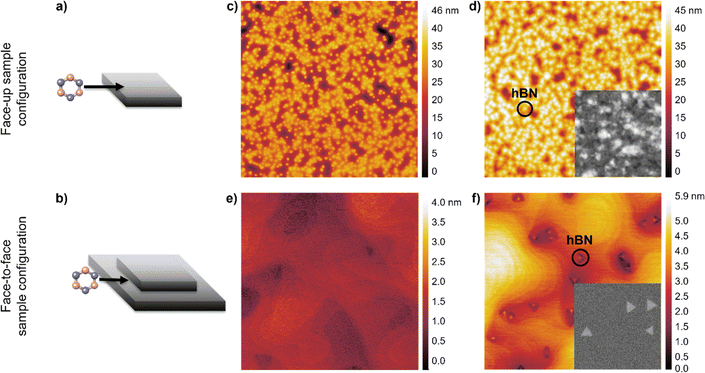
First, we find that suppressing Ge sublimation, which occurs readily under high vacuum at the growth temperature of 920 °C, is crucial for growing high-quality hBN. In Fig. 1, we compare two different substrate configurations: a face-up configuration, in which the growth surface is exposed to high vacuum (Fig. 1a), and a face-to-face configuration, in which the growth surface is placed in direct contact with another piece of Ge (Fig. 1b).When Ge(001) is annealed under high vacuum in the face-up configuration, Ge sublimes, and the surface roughens considerably (Fig. 1c, RMS roughness = 5.6 nm). The roughening of the surface results in a high hBN nucleation density, non-triangular morphology, and non-uniform thickness of hBN islands grown in this configuration (Fig. 1d). These results may explain the high nucleation density observed for multilayer hBN grown on Ge on Si(001) from borazine via high-vacuum CVD reported previously.18 Additionally, thermal etch pits that are over 1 μm deep form after just 30 minutes of annealing (Fig. S1†). These pits would interfere significantly with the growth and coalescence of a monolayer of hBN. In contrast, when Ge(001) is annealed under high vacuum in the face-to-face configuration, the surface is significantly smoother (Fig. 1e, RMS roughness = 0.3 nm). We attribute this smoothness to the suppression of Ge sublimation due to the buildup of Ge vapor pressure between the two faces. hBN islands grown in this configuration have lower nucleation density and triangular morphology (Fig. 1f), indicating marked improvement over hBN grown in the face-up configuration.
The effect of Ge surface orientation on hBN island orientation
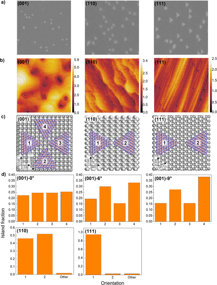
Using a face-to-face configuration, a borazine partial pressure of 1 × 10⁻¹⁰ torr, and a growth time of 30 minutes, we grow hBN islands on Ge(001), (110), and (111), as well as Ge(001) intentionally miscut by 6° and 9° toward Ge[111] and show that hBN island orientations are highly dependent on the Ge surface orientation. We use a low borazine partial pressure of 1 × 10⁻¹⁰ torr because the resulting slow growth rate (∼100 to 200 nm min−1) and low nucleation density (∼1 to 2 μm−2) result in triangular, mostly non-overlapping islands whose orientations can be easily observed and quantified using SEM. Prior work by Yin et al. indicates that hBN edges on Ge(001) and (110) are aligned along the zigzag direction.16 We anticipate hBN edges to be N-terminated based on theoretical predictions by Zhang et al. for hBN on Cu and Ni,26 which are weakly interacting catalysts like Ge. Fig. 2a shows SEM of the hBN islands, and Fig. 2b shows AFM height maps of the same samples as in Fig. 2a, indicating that the Ge(110) and (111) surfaces are significantly smoother than the (001) surface after the growth of hBN islands.On Ge(001), (001)-6°, and (001)-9°, hBN islands are triangular and have four preferred orientations, each having an edge parallel to Ge[110] or [1![[1 with combining macron]](https://www.rsc.org/images/entities/char_0031_0304.gif) 0] (Fig. 2a–c). When the miscut angle is approximately 0°, the islands are distributed evenly between the four preferred orientations, as previously reported by Yin et al.16 When the miscut angle is increased to 6° and then 9°, the distribution shifts such that orientations where the island edge is parallel to Ge[1
0] (Fig. 2a–c). When the miscut angle is approximately 0°, the islands are distributed evenly between the four preferred orientations, as previously reported by Yin et al.16 When the miscut angle is increased to 6° and then 9°, the distribution shifts such that orientations where the island edge is parallel to Ge[1![[1 with combining macron]](https://www.rsc.org/images/entities/char_0031_0304.gif) 0] are preferred, with an increasing preference for the islands to be pointed downhill (Fig. 2d). This is likely due to the preferential nucleation of hBN islands off of Ge step edges in the downhill direction. Ultimately, it may be possible to grow unidirectionally aligned hBN islands by increasing the miscut angle further.
0] are preferred, with an increasing preference for the islands to be pointed downhill (Fig. 2d). This is likely due to the preferential nucleation of hBN islands off of Ge step edges in the downhill direction. Ultimately, it may be possible to grow unidirectionally aligned hBN islands by increasing the miscut angle further.
On Ge(110), hBN islands have two preferred orientations, each having an edge parallel to Ge[1![[1 with combining macron]](https://www.rsc.org/images/entities/char_0031_0304.gif) 0], similar to the observations made by Yin et al. and Zhang et al.16,17 The islands are distributed approximately evenly between the two preferred orientations (Fig. 2d), which is expected on the two-fold symmetrical Ge(110) surface.
0], similar to the observations made by Yin et al. and Zhang et al.16,17 The islands are distributed approximately evenly between the two preferred orientations (Fig. 2d), which is expected on the two-fold symmetrical Ge(110) surface.
On Ge(111), triangular hBN islands are expected to have six (or two unique) preferred orientations due to the six-fold symmetry of the Ge(111) surface. However, we observe that one of the two unique orientations is heavily favored, and 95% of the islands are unidirectionally aligned (Fig. 1a–d). This unexpected result may be explained by a theory proposed by Chen et al., in which asymmetry at opposing Cu(111) step edges and in their binding energies causes hBN nuclei to dock preferentially on one side of the steps, resulting in the unidirectional alignment of hBN islands on Cu(111).2 A similar asymmetry at opposing step edges is seen on Ge(111) (Fig. S2†), which seems to have the same effect as on Cu(111). With further tuning of growth parameters and understanding of hBN nuclei-step docking on Ge, it may be possible to grow single crystal hBN on Ge(111).
Growth and characterization of hBN monolayers on single-crystalline Ge
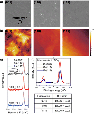
By extending the growth time from 30 minutes to 10 hours, we are able to grow monolayer hBN on Ge(001), (110), and (111). Wrinkles originating from the difference in the coefficient of thermal expansion of hBN and Ge are seen in SEM (Fig. 3a) and AFM (Fig. 3b), indicating that the surface is fully covered. In addition, AFM shows that after hBN growth, the Ge(110) and (111) surfaces are atomically flat, but the Ge(001) surface is nano-faceted (Fig. 3b). As a result, hBN grown on Ge(110) and (111) is much smoother than hBN grown on Ge(001). These surface topographies are similarly observed for graphene grown on Ge(001), (110), and (111).27 For films transferred to SiO2/Si, Raman peaks are observed at 1370 cm−1 with full-widths at half-maximum of ≈19 cm−1 (Fig. 3c). These data have not previously been reported for hBN monolayers on Ge.Transferring the films also allows for a more accurate measurement of the film stoichiometry by removing potential effects from the substrate, for example nitridation of the Ge surface during growth as proposed by Yin et al.16 XPS reveals that the films are stoichiometric (B![[thin space (1/6-em)]](https://www.rsc.org/images/entities/char_2009.gif) :
:![[thin space (1/6-em)]](https://www.rsc.org/images/entities/char_2009.gif) N ≈ 1
N ≈ 1![[thin space (1/6-em)]](https://www.rsc.org/images/entities/char_2009.gif) :
:![[thin space (1/6-em)]](https://www.rsc.org/images/entities/char_2009.gif) 1) (Fig. 3d). It is not clear if the few percent overabundance of N in hBN monolayers grown on Ge(001) and Ge(111) is an accurate reflection of a small degree of non-stoichiometry or are indicative of systematic error in our B
1) (Fig. 3d). It is not clear if the few percent overabundance of N in hBN monolayers grown on Ge(001) and Ge(111) is an accurate reflection of a small degree of non-stoichiometry or are indicative of systematic error in our B![[thin space (1/6-em)]](https://www.rsc.org/images/entities/char_2009.gif) :
:![[thin space (1/6-em)]](https://www.rsc.org/images/entities/char_2009.gif) N ratio determination.
N ratio determination.
Characterization and reduction of pinhole defects in hBN monolayers
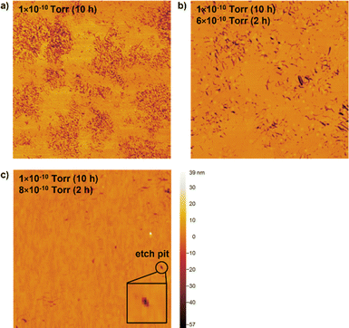
To further characterize the quality and completeness of the hBN monolayers, the presence of pinhole defects in hBN films grown on Ge(110) is quantified by dipping them into a Ge etchant (0.02 M FeCl3). The etchant diffuses through pinholes in the hBN and creates etch pits in the underlying Ge that can then be visualized with AFM. (In contrast, etch pits are not formed when a bare Ge surface is dipped into the etchant, see Fig. S3.†) We find that while hBN films grown under many conditions appear to be complete monolayers as assessed by SEM, AFM, and Raman, these hBN films are plagued by a high density of pinhole defects (Fig. 4a). In many hBN applications, such as the use of hBN as passivation layers for air-sensitive materials,28,29 ultrasmooth and clean substrates for reducing charge or exciton scattering,30,31 and barrier layers for controlling interlayer excitons,32 these pinholes are likely to be detrimental to performance.To reduce the pinhole density and thus improve film quality, we grow hBN with the same borazine partial pressure as before (1 × 10⁻¹⁰ torr) but, at the end of growth, supply a burst of borazine at a higher partial pressure (6–8 × 10⁻¹⁰ torr) for 2 h (Fig. S4,† 4b and c). A two-step process is required because using a high borazine partial pressure from the beginning results in poorer crystallographic alignment (Fig. S5†). Using a two-step process allows us to maintain the alignment, low nucleation density, and slow growth rate of hBN islands until the surface is nearly completely covered. Then, increasing the borazine partial pressure increases the probability of borazine molecules or molecular fragments encountering and subsequently healing pinhole defects in the hBN monolayer. We find that this method ultimately decreases the density of pinhole defects to ∼0.7 μm−2 (Fig. 4c). The pinhole densities measured for highly optimized graphene growth on Ge(110) are ∼0.01 per μm2.33
Growth of hBN on Ge epilayers on Si
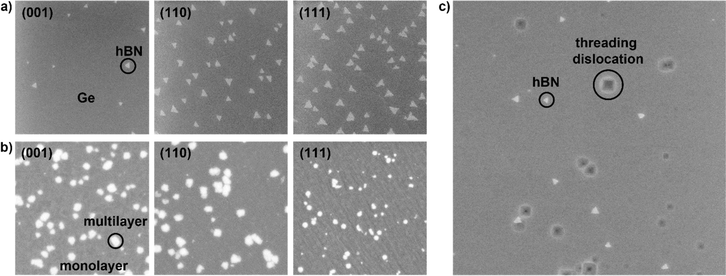
To enhance the compatibility of hBN growth with semiconductor industrial processes, we demonstrate the growth of hBN on epilayers of Ge on Si(001), (110), and (111). We find that hBN islands grown on epilayers of Ge on Si have the same rotational alignment and similar morphology to islands grown on equivalent Ge surfaces, indicating that growth is comparable on the two substrates (Fig. 5a). However, small differences in the hBN island morphology specifically on Ge/Si(111) are observed, possibly due to the high initial roughness of the Ge/Si(111) surface (Fig. S6†). Additionally, we dip the hBN islands grown on Ge/Si(001) into Secco etch solution, which selectively creates etch pits at threading dislocations in the Ge epilayer.25 We find that the location of these threading dislocations has no correlation with where hBN islands nucleate (Fig. 5c).The growth of monolayer hBN is complicated by the diffusion of Si through Ge at high temperatures. When Si segregates at the Ge surface, it roughens the surface34 and disrupts hBN growth, likely due to its noncatalytic nature and requirements for higher growth temperatures35 (Fig. S7†). To minimize Si diffusion, we increase the borazine partial pressure from 1 × 10⁻¹⁰ to 6 × 10⁻¹⁰ torr so that growth can be completed within 6 hours instead of 10. While this does enable faster coalescence, we also observe the formation of multilayer hBN islands, with coverage ranging from 2 to 5% and heights ranging from 1 to 8 nm (Fig. 5b).
Conclusions
In summary, suppressing Ge sublimation is essential for growing high-quality hBN on Ge via high-vacuum CVD. Using a borazine precursor, we show that the orientational alignment of hBN correlates strongly with the surface orientation and miscut angle of Ge. Remarkably, 95% of hBN nuclei are unidirectionally aligned on Ge(111), which presents a promising path toward the growth of single-crystalline hBN on a semiconducting substrate. Despite hBN monolayers appearing to be full coverage and high quality as characterized by SEM, AFM, and Raman spectroscopy, pinhole defects can be prevalent. However, the density of pinhole defects can be significantly reduced by introducing a burst of borazine precursor toward the end of the hBN growth process. These findings, along with successful hBN growth on Ge epitaxial layers on Si, hold considerable promise for the integration of hBN into advanced microelectronics.Data availability
The data supporting this article have been included within the manuscript and electronic ESI.†Author contributions
KAS: conceptualization, methodology, investigation, and writing – original draft. SL: methodology and validation. WCW: resources. YY: resources and writing – review and editing. MSA: conceptualization, writing – review and editing, supervision, and funding acquisition.Conflicts of interest
There are no conflicts of interest to declare.Acknowledgements
Investigation of Ge orientation dependence, growth on Ge epilayers on Si, Raman spectroscopy, XPS, and etch pit characterization supported by the U.S. Department of Energy, Office of Science, Basic Energy Sciences, under Grant No. DE-SC0016007 (K. A. S., M. S. A.). Early studies on effects of Ge sublimation, XPS, and CVD tool development supported by the U.S. National Science Foundation Grant No. DMR-2102643 (S. L., M. S. A.). The authors acknowledge the use of facilities and instrumentation at the UW-Madison Wisconsin Centers for Nanoscale Technology, which is partially supported by the NSF through the University of Wisconsin Materials Research Science and Engineering Center (DMR-1720415). Support from a U.S. NSF Graduate Research Fellowship under Grant No. DGE-1747503 and from a PPG Industries Graduate Fellowship is also acknowledged (K. A. S.).References
- N. Briggs, S. Subramanian, Z. Lin, X. Li, X. Zhang, K. Zhang, K. Xiao, D. Geohegan, R. Wallace, L.-Q. Chen, M. Terrones, A. Ebrahimi, S. Das, J. Redwing, C. Hinkle, K. Momeni, A. Van Duin, V. Crespi, S. Kar and J. A. Robinson, 2D Mater., 2019, 6, 022001 CrossRef CAS.
- T. A. Chen, C. P. Chuu, C. C. Tseng, C. K. Wen, H. S. P. Wong, S. Pan, R. Li, T. A. Chao, W. C. Chueh, Y. Zhang, Q. Fu, B. I. Yakobson, W. H. Chang and L. J. Li, Nature, 2020, 579, 219–223 CrossRef CAS PubMed.
- L. Wang, X. Xu, L. Zhang, R. Qiao, M. Wu, Z. Wang, S. Zhang, J. Liang, Z. Zhang, Z. Zhang, W. Chen, X. Xie, J. Zong, Y. Shan, Y. Guo, M. Willinger, H. Wu, Q. Li, W. Wang, P. Gao, S. Wu, Y. Zhang, Y. Jiang, D. Yu, E. Wang, X. Bai, Z. J. Wang, F. Ding and K. Liu, Nature, 2019, 570, 91–95 CrossRef CAS PubMed.
- S. Joshi, D. Ecija, R. Koitz, M. Iannuzzi, A. P. Seitsonen, J. Hutter, H. Sachdev, S. Vijayaraghavan, F. Bischoff, K. Seufert, J. V. Barth and W. Auwärter, Nano Lett., 2012, 12, 5821–5828 CrossRef CAS.
- X. Song, J. Gao, Y. Nie, T. Gao, J. Sun, D. Ma, Q. Li, Y. Chen, C. Jin, A. Bachmatiuk, M. H. Rümmeli, F. Ding, Y. Zhang and Z. Liu, Nano Res., 2015, 8, 3164–3176 CrossRef CAS.
- P. Arias, A. Ebnonnasir, C. V. Ciobanu and S. Kodambaka, Nano Lett., 2020, 20, 2886–2891 CrossRef CAS PubMed.
- Y. Uchida, T. Iwaizako, S. Mizuno, M. Tsuji and H. Ago, Phys. Chem. Chem. Phys., 2017, 19, 8230–8235 RSC.
- K. K. Kim, A. Hsu, X. Jia, S. M. Kim, Y. Shi, M. Hofmann, D. Nezich, J. F. Rodriguez-Nieva, M. Dresselhaus, T. Palacios and J. Kong, Nano Lett., 2012, 12, 161–166 CrossRef PubMed.
- M. P. Levendorf, C.-J. Kim, L. Brown, P. Y. Huang, R. W. Havener, D. A. Muller and J. Park, Nature, 2012, 488, 627–632 CrossRef CAS PubMed.
- S. Wang, X. Wang and J. H. Warner, ACS Nano, 2015, 9, 5246–5254 CrossRef CAS.
- A. Yan, J. Jr. Velasco, S. Kahn, K. Watanabe, T. Taniguchi, F. Wang, M. F. Crommie and A. Zettl, Nano Lett., 2015, 15, 6324–6331 CrossRef CAS PubMed.
- M. Okada, T. Sawazaki, K. Watanabe, T. Taniguch, H. Hibino, H. Shinohara and R. Kitaura, ACS Nano, 2014, 8, 8273–8277 CrossRef CAS PubMed.
- M. Alahmadi, F. Mahvash, T. Szkopek and M. Siaj, RSC Adv., 2021, 11, 16962–16969 RSC.
- S. J. U. White, T. Yang, N. Dontschuk, C. Li, Z.-Q. Xu, M. Kianinia, A. Stacey, M. Toth and I. Aharonovich, Light: Sci. Appl., 2022, 11, 186 CrossRef CAS PubMed.
- N. Chejanovsky, A. Mukherjee, J. Geng, Y.-C. Chen, Y. Kim, A. Denisenko, A. Finkler, T. Taniguchi, K. Watanabe, D. B. R. Dasari, P. Auburger, A. Gali, J. H. Smet and J. Wrachtrup, Nat. Mater., 2021, 20, 1079–1084 CrossRef CAS.
- J. Yin, X. Liu, W. Lu, J. Li, Y. Cao, Y. Li, Y. Xu, X. Li, J. Zhou, C. Jin and W. Guo, Small, 2015, 11, 5375–5380 CrossRef CAS PubMed.
- C. Zhang, B. Gao, Y. Ran, Z. Shi, H. Zhu, H. Zhang, J. Liu, B. Yang, Z. Liu, T. Wu and X. Xie, 2D Mater., 2021, 8, 035041 CrossRef CAS.
- M. Franck, J. Dabrowski, M. A. Schubert, C. Wenger and M. Lukosius, Nanomaterials, 2022, 12, 3260 CrossRef CAS PubMed.
- V. Babenko, G. Lane, A. A. Koos, A. T. Murdock, K. So, J. Britton, S. S. Meysami, J. Moffat and N. Grobert, Sci. Rep., 2017, 7, 14297 CrossRef PubMed.
- J. H. Park, A. Y. Lu, M. M. Tavakoli, N. Y. Kim, M. H. Chiu, H. Liu, T. Zhang, Z. Wang, J. Wang, L. G. P. Martins, Z. Luo, M. Chi, J. Miao and J. Kong, Nano Lett., 2023, 23, 4741–4748 CrossRef CAS PubMed.
- Y. Yamamoto, P. Zaumseil, T. Arguirov, M. Kittler and B. Tillack, Solid-State Electron., 2011, 60, 2–6 CrossRef CAS.
- Y. Yamamoto, P. Zaumseil, M. A. Schubert and B. Tillack, Semicond. Sci. Technol., 2018, 33, 124007 CrossRef.
- Y. Yamamoto, W. C. Wen, M. A. Schubert, C. Corley-Wiciak and B. Tillack, ECS J. Solid State Sci. Technol., 2023, 12, 023014 CrossRef.
- L. Gao, W. Ren, H. Xu, L. Jin, Z. Wang, T. Ma, L. P. Ma, Z. Zhang, Q. Fu, L. M. Peng, X. Bao and H. M. Cheng, Nat. Commun., 2012, 3, 699 CrossRef PubMed.
- A. Abbadie, F. Allibert and F. Brunier, Solid-State Electron., 2009, 53, 850–857 CrossRef CAS.
- Z. Zhang, Y. Liu, Y. Yang and B. I. Yakobson, Nano Lett., 2016, 16, 1398–1403 CrossRef CAS PubMed.
- R. M. Jacobberger, D. E. Savage, X. Zheng, P. Sookchoo, R. Rojas Delgado, M. G. Lagally and M. S. Arnold, Chem. Mater., 2022, 34, 6769–6778 CrossRef CAS.
- H. Arora, Y. Jung, T. Venanzi, K. Watanabe, T. Taniguchi, R. Hübner, H. Schneider, M. Helm, J. C. Hone and A. Erbe, ACS Appl. Mater. Interfaces, 2019, 11, 43480–43487 CrossRef CAS PubMed.
- A. J. Cho and J. Y. Kwon, ACS Appl. Mater. Interfaces, 2019, 11, 39765–39771 CrossRef CAS.
- C. R. Dean, A. F. Young, I. Meric, L. Wang, S. Sorgenfrei, K. Watanabe, T. Taniguchi, P. Kim, K. L. Shepard and J. Hone, Nat. Nanotechnol., 2010, 5, 722–726 CrossRef CAS PubMed.
- N. Fang, K. Otsuka, A. Ishii, T. Taniguchi, K. Watanabe, K. Nagashio and Y. K. Kato, ACS Photonics, 2020, 7, 1773–1779 CrossRef CAS.
- E. V. Calman, M. M. Fogler, L. V. Butov, S. Hu, A. Mishchenko and A. K. Geim, Nat. Commun., 2018, 9, 1895 CrossRef CAS PubMed.
- R. M. Jacobberger, M. J. Dodd, M. Zamiri, A. J. Way, M. S. Arnold and M. G. Lagally, ACS Appl. Nano Mater., 2019, 2, 4313–4322 CrossRef CAS.
- V. Saraswat, Y. Yamamoto, H. J. Kim, R. M. Jacobberger, K. R. Jinkins, A. J. Way, N. P. Guisinger and M. S. Arnold, J. Phys. Chem. C, 2019, 123, 18445–18454 CrossRef CAS.
- X. Chen, C. Tan, X. Liu, K. Luan, Y. Guan, X. Liu, J. Zhao, L. Hou, Y. Gao and Z. Chen, J. Mater. Sci.: Mater. Electron., 2021, 32, 3713–3719 CrossRef CAS.
Footnote |
| † Electronic supplementary information (ESI) available: Additional SEM/AFM data and schematics. See DOI: https://doi.org/10.1039/d4ra03704a |
| This journal is © The Royal Society of Chemistry 2024 |

