
 Open Access Article
 This Open Access Article is licensed under a Creative Commons Attribution-Non Commercial 3.0 Unported Licence
Formation of oxygen protective layer on monolayer MoS2 via low energy electron irradiation†
Aissara Rasritat ,
Manunya Tapakidareekul,
Kritsana Saego,
Worawat Meevasana and
Sorawis Sangtawesin*
,
Manunya Tapakidareekul,
Kritsana Saego,
Worawat Meevasana and
Sorawis Sangtawesin*
School of Physics, Suranaree University of Technology, Nakhon Ratchasima 30000, Thailand. E-mail: sorawis.s@g.sut.ac.th
First published on 11th July 2024
Abstract
Monolayer molybdenum disulfide (MoS2) semiconductors are the new generation of two-dimensional materials that possess several advantages compared to graphene due to their tunable bandgap and high electron mobility. Several approaches have been used to modify their physical properties for optical device applications. Here, we report a facile and non-destructive surface modification method for monolayer MoS2 via electron irradiation at a low, 5 kV accelerating voltage. After electron irradiation, the results of Raman and photoluminescence spectroscopy confirmed that the structure remains unchanged. However, when the modified surface was illuminated with a 532 nm laser for a prolonged period, the PL intensity was quenched as a result of oxygen desorption. Interestingly, the PL intensity can be recovered when left in ambient conditions for 10 h. The analysis of the PL spectrum revealed a decrease of trion, which is consistent with the readsorbed O2 molecules on the surface that deplete electrons and lead to PL recovery. We attribute this effect to the enhancement of the n-type character of monolayer MoS2 after electron irradiation. The sensitive nature of the modified surface to oxygen suggests that this approach may be used as a tool for the fabrication of MoS2 oxygen sensors.
Introduction
Two-dimensional transition metal dichalcogenides (TMDs) are an emerging class of materials with highly desirable properties for investigating novel physical phenomena and exploring various applications. Monolayer molybdenum disulfide (MoS2) is one of the most extensively studied TMDs owing to its distinctive structural and physical properties.1–4 Specifically, molybdenum (Mo) and sulfur (S) atoms are arranged in a honeycomb-like network by covalent bond in a sequence of S–Mo–S and form a monolayer structure of MoS2, where each layer is stacked by a weak van der Waals force.5 When thinned down from bulk into a monolayer structure, MoS2 exhibits photoluminescence (PL) due to transition from indirect band gap (1.2 eV) to direct band gap (1.8 eV),6 which enhances both light absorption and emission. This unique transition makes MOS2 effective for applications such as photocatalysts,7 sensors,8–10 and electronic devices.11–14 Although several methods have been developed to synthesize monolayer MoS2, chemical vapor deposition (CVD) technique is one of the most promising processes that helps obtain high-quality materials with a large area.15 Experimental studies have shown that MoS2 may contain several types of defects, including S monovacancy, S divacancy, antisite defects, and MoSx complexes.16 In CVD process, the most commonly found defect is S monovacancy, which exhibits n-type features due to its lowest formation energy compared to the other defects.17,18 According to various studies, the S vacancy generates trap states that reduce radiative recombination, leading to PL suppression.19 As a result, these defects must be minimized or subsequently repaired to maintain the optical properties of monolayer MoS2.Defect passivation approaches have been extensively developed to overcome this issue. It has been reported that the original PL spectrum of monolayer MoS2 can be recovered by both chemical and physical adsorption of oxygen molecules (O2) on the S vacancy.20 The adsorbed O2 molecules will withdraw electrons from the monolayer MoS2 owing to the heavy p-type nature of O2 molecules. This charge transfer process depletes n-type property and stabilizes excitons that create a new gap state, resulting in an increase of radiative recombination.21–24 In 2017, Zhao et al. used first-principles calculations to examine the effect of transition metal doping on the surface of the monolayer MoS2 and found that the doping of transition metal can decrease the adsorption energy of O2 by providing an additional electron from the 3d orbital of the transition metal into 2π* orbital of the O2 molecule.25 Therefore, it can be expected that an addition of excess electron will enhance O2 physical adsorption, leading to PL recovery.
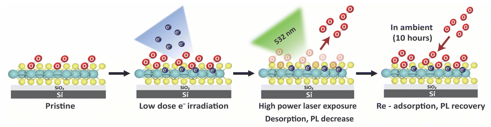
Inspired by the abovementioned finding, this work investigates the potential of direct electron passivation on the surface of monolayer MoS2 as a technique for enhancing O2 adsorption. To remove the original O2 adsorbed on the surface of this material, a focused 532 nm laser was used to clean the sample. The PL intensities were evaluated by confocal microscopy during the O2 desorption and re-adsorption processes (Scheme 1).
 | ||
| Scheme 1 Schematic demonstration of O2 physical adsorption on the modified surface of monolayer MoS2. | ||
The optical results show that the irradiated electrons are permanently passivated on the surface of monolayer MoS2, which led to the ability to re-adsorb O2 following 532 nm exposure, as evidenced by the PL recovery.
Experimental
Sample
Monolayer MoS2 was purchased from 2D Semiconductors, USA. This hexagonal phase, undoped monolayer MoS2 was prepared on a SiO2/Si substrate using atmospheric pressure chemical vapor deposition (APCVD). The monolayer uniformly covers the entire substrate with a surface roughness of <0.2 nm and 99.9995% purity as determined by nano-SIMS.Electron beam irradiation
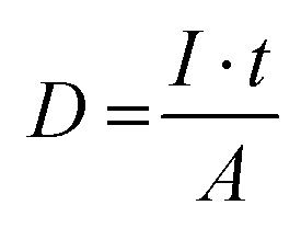
Electron beam irradiation was performed in a Zeiss model Auriga. The electron dose was varied by adjusting the scanning time while fixing the scanning area, ensuring an accelerating voltage of 5 kV and a specimen current of 264 pA. The electron dose (D) for irradiation was calculated by the number of electrons received per unit area, as shown below:where I is the specimen current, t is the total scanning time, and A is the scanning area.
Confocal PL measurement
PL measurements were carried out at room temperature using a home-built confocal microscope equipped with a 100× objective lens (Olympus MPLanFL N 100×). A 532 nm excitation laser (Coherent OBIS 532), with an approximate spot size of 1 μm was used for sample exposure. A relatively low laser power of 118 μW (at the back aperture of the objective lens) was used for scanning to avoid sample damage. Photoluminescence was collected from the sample with the same objective and was separated from the excitation with a 567 nm dichroic mirror (Thorlabs DMLP567) and was filtered with a 600 nm long-pass filter (Thorlabs FELH0600). Finally, the signals were divided into two parts using a fiber beam splitter for intensity measurements with an avalanche photodiode detector (APD), which yields the pixel intensity in terms of the photon count rate (Hz), and for spectrum analysis with a spectrometer (Andor DU940P-BU2, 300 L mm−1 grating, Kymera 328i CCD). The long-pass filter was removed during spectrum analysis.The effect of gas species on the PL variation of MoS2 was investigated by low electron dose condition again by exposing the sample with a high-power laser in N2 atmosphere before changing to ambient conditions. To perform the experiment with N2, we enclosed the sample area of the microscope and continuously flowed nitrogen gas into the enclosure with the tank outlet pressure set between 12 and 16 psi to ensure no ambient air can leak back into the enclosure (Fig. S1 and S2†). Then, the high-power 532 nm laser at 14.7 mW was exposed to the sample for 10 s, and we monitored the PL intensity and spectra in N2 atmosphere for 10 h. Finally, we turned off the gas flow and let the ambient air leak back into the enclosure while monitoring the PL for another 10 h.
Raman measurement
Raman measurements were obtained by a Bruker Optics SENTERRA II Dispersive Raman Microscope under ambient conditions. The 532 nm excitation laser was set at 0.5 mW to avoid laser-induced damage. The excitation is focused onto the sample with a 100× objective, and a grating with 1200 L mm−1 was used to perform spectra imaging, with a nominal spectral resolution of 0.5 cm−1.Results and discussion
The monolayer MoS2 sample was irradiated with an electron beam on the surface at different regions (Fig. 1). The accelerating voltage was fixed at a low value of 5 kV to avoid generation of additional defects.26 Two different electron doses, D = 0.3 × 10³ μC cm−2 and D = 5.3 × 10³ μC cm−2, referred to as the low electron dose and the high electron dose, respectively, were used to investigate the effect of the dose on the PL properties.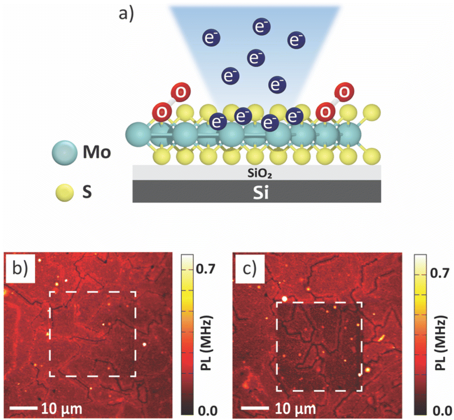 | ||
| Fig. 1 (a) Schematic illustration of electron beam irradiation on monolayer MoS2 by SEM with 5 kV accelerating voltage. Confocal PL intensity images of the irradiated samples with different electron irradiation doses (b) D = 0.3 × 10³ μC cm−2 and (c) D = 5.3 × 10³ μC cm−2, respectively. The irradiation areas are shown in dash line boxes. | ||
The samples were characterized using optical spectroscopic techniques, to determine the effect of electron irradiation on structural and chemical properties of monolayer MoS2. We can observe that the PL intensity from the MoS2 after low electron dose condition is the same as that of the surrounding pristine area (Fig. 1b). However, we observed a photobleaching effect in the area exposed to a high electron dose (Fig. 1c). Photobleaching is a situation where the MoS2 surface undergoes a permanent loss of fluorescence capability owing to chemical damage,27 resulting in a decrease in PL intensity.
It is well-known that monolayer MoS2 prepared by CVD approach generally exhibits S vacancy with other types of defects.23,28,29 Therefore, the investigation of monolayer MoS2 structure prior to electron irradiation is necessary. Typically, Raman spectroscopy is used to investigate defects such as S vacancy, which is created by electron irradiation.14 Moreover, it can be used to determine the number of layers and uniformity of monolayer MoS2 samples by evaluating the difference in energy of the vibrational modes. According to Raman spectra in Fig. 2a, the characteristic peaks appear at ∼385 and ∼403 cm−1, corresponding to in-plane E2 mode and out-of-plane A1 mode, respectively. The peak positions for E2 and A1 modes were determined by fitting two Lorentzian functions to the spectra. The difference between these two modes is 20.5 cm−1, consistent with a monolayer MoS2.30 In the case where the MoS2 is irradiated with high electron energy, more defects may be generated due to the loss of S atoms. The formation of S vacancy will reduce the molecular symmetry of the monolayer MoS2 and lead to the change of symmetry assignment in Raman vibrational modes. Here, we show that after electron irradiation, the peak positions remained unchanged in both low and high electron dose conditions. Hence, it can be assumed that electron irradiation did not generate additional S vacancies or structural alterations at the chosen 5 kV acceleration voltage.
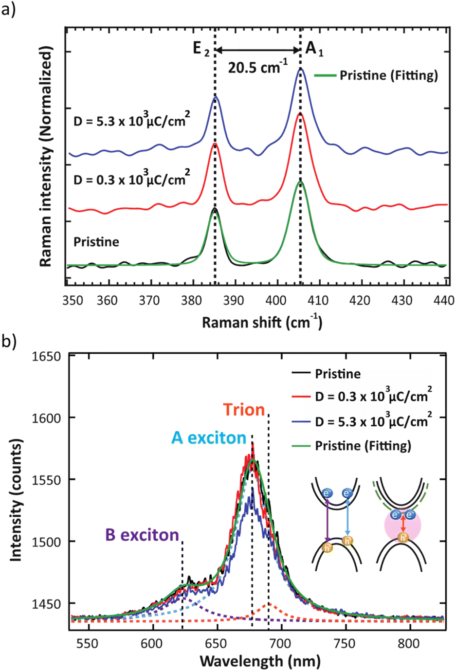 | ||
| Fig. 2 (a) Raman spectra of monolayer MoS2 without electron irradiation (black line), D = 0.3 × 10³ μC cm−2 (red line), and D = 5.3 × 10³ μC cm−2 (blue line) respectively. The left and right dashed line indicate the position of E2 (in-plane vibration) and A1 (out-of-plane vibration) peaks. (b) Comparison of the PL spectra of monolayer MoS2 without electron irradiation (black line), D = 0.3 × 10³ μC cm−2 (red line), and D = 5.3 × 10³ μC cm−2 (blue line), respectively. Each spectrum consists of three components including B exciton peak at 623 nm, A exciton peak at 677 nm, and trion peak at 690 nm. All PL peaks were fitted by Lorentzian function (green lines). | ||
In the PL spectra (Fig. 2b), the trion peak was observed at 690 nm. This trion state is attributed to two electrons in a hole or negatively charged exciton.31 An optical band gap of 677 nm was observed, which confirmed the monolayer thickness of the sample.32,33 After electron irradiation, we do not observe any shift in the PL spectra that has been previously associated with the generation of S vacancies,34 thus confirming that the structure remained unchanged after electron irradiation. We note that the lower intensity of the unnormalized PL spectra for the high electron dose condition is attributed to photobleaching. To study the O2 desorption and re-adsorption processes, we selectively illuminated some spots on the surface with a high-power 532 nm laser (14.7 mW) as shown in Fig. 3a. Normally, this high-power illumination is performed to clean adsorbed gas (N2, O2 and H2O) away from the surface of monolayer MoS2. Fig. 3e–g show the quenching of PL intensity after laser illumination, which is consistent with the O2 desorption. Then, after storing in ambient conditions for 10 h, the PL intensities of the pristine and high electron dose conditions remained quenched (Fig. 3h and j), whereas the low electron dose condition exhibited PL recovery (Fig. 3i). To quantitatively study the recovery, relative PL intensity was calculated by dividing the PL intensity of the quenched area after exposure by the PL intensity of the same area prior to the exposure. In the case of the pristine sample, the relative PL intensity of the illuminated area decreased by 50%, and there was no recovery of PL intensity with ambient storage (Fig. 4a). We attribute this behavior to the lack of active sites for gas adsorption on the cleaned surface.35
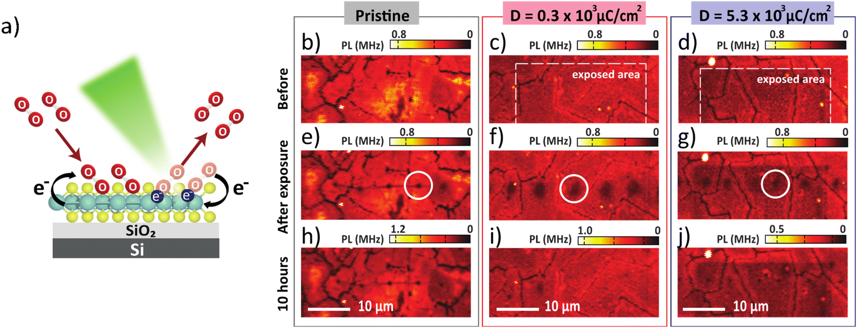 | ||
| Fig. 3 (a) Schematic illustration of monolayer MoS2 which was irradiated by 532 nm laser at 14.7 mW under ambient atmosphere. Confocal images of monolayer MoS2 before laser illumination of (b) pristine, (c) D = 0.3 × 10³ μC cm−2 (white box), and (d) D = 5.3 × 10³ μC cm−2, respectively. After laser illumination (14.7 mW) for 10 s the PL images show in (e) pristine, (f) electron dose 0.3 × 10³ μC cm−2, and (g) 5.3 × 10³ μC cm−2. After storing in the ambient air for 10 hours in the low electron dose condition, the quenching area disappears, as shown in (i), and is still unchanged in (h) pristine and (j) high electron dose. Dashed white boxes indicate the electron exposed areas and the white circles indicate the high-power laser exposed areas used for PL spectra measurements. | ||
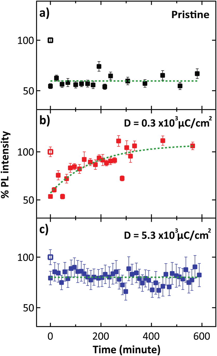 | ||
| Fig. 4 Relative PL intensity with varying different conditions consists of (a) pristine, (b) electron dose of 0.3 × 10³ μC cm−2, and (c) 5.3 × 10³ μC cm−2, at the spots indicated by white circles in Fig. 3(e)–(g), respectively. | ||
However, the PL recovery can be observed in the case of low electron dose condition, where the PL intensity gradually increased to close to the original state after storing the sample in ambient conditions for 10 h (Fig. 4b). In this case, we hypothesized that the irradiation provides electronic charge on the surface of MoS2, which stimulates gas adsorption.35,36 Then, the charge transfer from the sample to the gas molecule can occur, leading to PL recovery. In the high electron dose condition, however, the original PL intensity cannot be recovered, and the quenching area remains unchanged during ambient storage. We attribute this irreversibility to photobleaching, which is evidenced by the lower initial PL intensity (dark patch in Fig. 3d). Moreover, we showed that exposure to a lower dose of D = 0.2 × 10³ μC cm−2 can result in PL recovery (Fig. S9†), while with the intermediate dose D = 2.0 × 10³ μC cm−2, where photobleaching starts to occur, the PL intensity cannot be recovered after high-power laser exposure (Fig. S11†).
To identify the gas species associated with the PL recovery mechanism, we further investigated the PL behavior of monolayer MoS2 irradiated by low electron dose condition again in the N2 atmosphere for 10 h, followed by ambient storage for another 10 h. As shown in Fig. 5, the PL intensity remained unchanged in the N2 atmosphere. However, the PL intensity gradually increased in the subsequent exposure to ambient conditions. This result suggests that the significant recovery of PL can be attributed to the physical adsorption of O2 molecules from the air, which then influences charge transfer from the MoS2 and then depletes the n-type character of the sample. This depletion weakens the electrostatic screening effect that would otherwise destabilize excitons.22 However, physical adsorption between gas molecules and the surface of MoS2 is formed by a weak van der Waals force, and under ambient conditions with approximately 78% N2 and 22% O2, these two types of gas may compete to adsorb on the surface of MoS2 leading to slow PL recovery.37
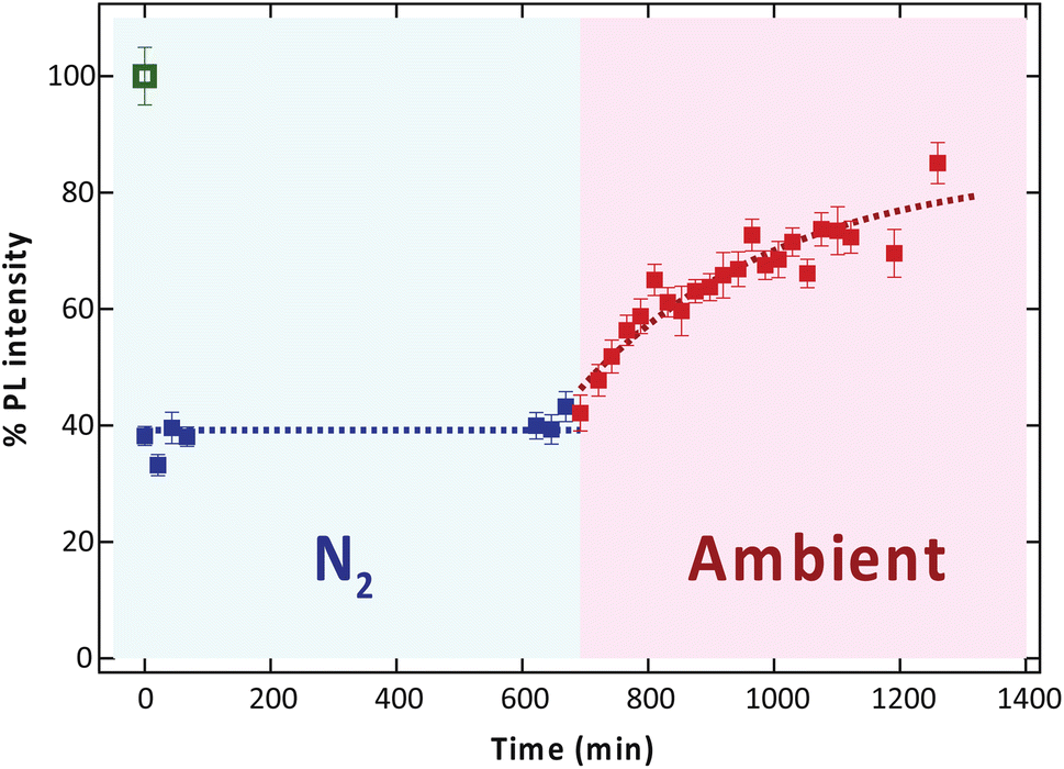 | ||
| Fig. 5 The relative PL intensity under N2 and ambient. | ||
To further analyze the effect of laser exposure, the spectra of the low-dose electron irradiated sample before and after exposure to the high-power laser are compared in Fig. 6. We found that the overall PL intensity decreased after exposure to the high-power laser, remained suppressed when kept in N2 for 10 h, and recovered after another 10 h of exposure to ambient conditions (Fig. 6a). Furthermore, red shift was observed in the overall PL spectrum after the exposure and the shift remained unchanged during which the sample was maintained in N2. Conversely, the spectrum shifted back to the original position after the subsequent ambient exposure.
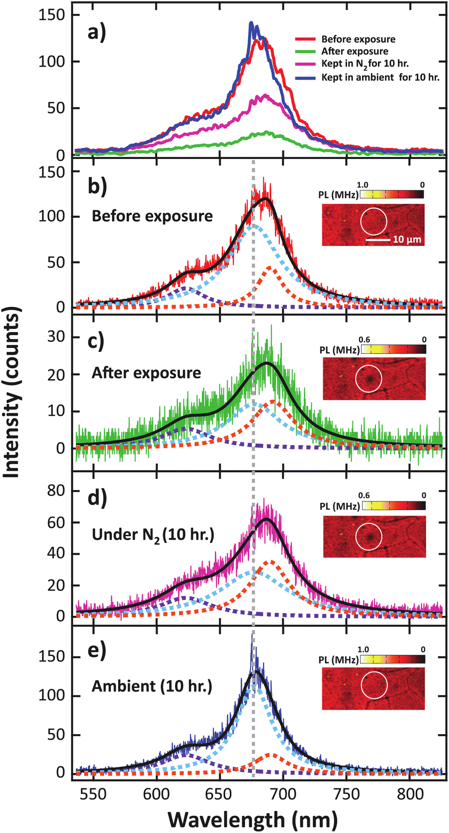 | ||
| Fig. 6 (a) The comparison of the background-subtracted PL spectra of monolayer MoS2 irradiated by low electron dose condition at the location indicated by the white circle, and the normalized PL spectra (b) before high power laser irradiation, (c) immediately after high power laser irradiation, (d) after 10 hour storage under N2, and (e) after another 10 hour storage in ambient conditions. The spectra in (a) are smoothed with 20-point boxcar averaging window for clarity. | ||
To investigate this phenomenon, we quantitatively analyzed the PL spectra by deconvoluting the data with three Lorentzian peaks associated with the A exciton, B exciton, and the trion, with the peak positions of A and B excitons fixed at 677 and 623 nm, respectively.31–33
The A and B excitons are the energy difference between the two resonances that results from spin–orbit coupling in the valence band.38,39 The transition probability of the A exciton is typically higher than that of the B exciton due to its lower energy.32 Consequently, the PL spectrum prominently exhibits the A exciton peak.
However, when the electron density is increased, the A exciton transition probability can be suppressed due to the formation of trion, which is the state in which two electrons are bound to a hole exhibiting finite binding energies.40–43 This process leads to a decrease in exciton absorption and a decrease in PL. Before high-power laser exposure (Fig. 6b), we determined the deconvoluted areas to be 72% A exciton, 12% B exciton, and 16% trion. After the exposure, while under a N2 atmosphere (Fig. 6c), the integrated A exciton intensity suddenly decreased to 46%, the trion intensity increased to 36%, while the B exciton remained low at 18%. The increase in the trion contribution is consistent with an n-type doping that was previously reported.31,44,45
During the 10 h of storage in N2, we did not observe any significant change in the exciton and trion intensity. Then, when the sample is re-exposed to ambient atmosphere, the trion intensity gradually decreased, along with the recovery of the A exciton intensity (Fig. 7a). These results confirmed the suppression of trion by the physical re-adsorption of O2 molecules.
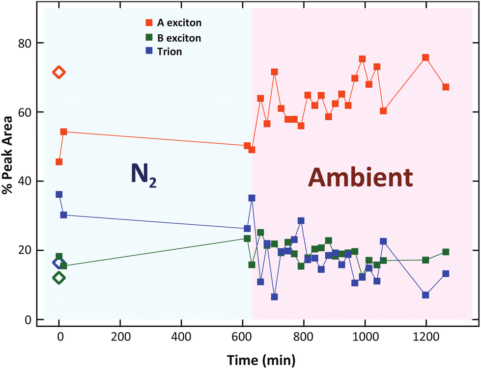 | ||
| Fig. 7 The relative peak area as a function of time under N2 and ambient conditions. Diamonds indicate the percentages before laser exposure. | ||
Conclusions
In this work, we show that the surface of a monolayer MoS2 can be simply modified by low-energy electron irradiation. Under appropriate conditions, the structure of the monolayer can be preserved, as confirmed by Raman and PL spectroscopy, and the passivated electrons can induce an n-type behavior in the MoS2. Consequently, the modified surface can efficiently adsorb O2 molecules from the atmosphere.Most importantly, the adsorption and desorption of O2 molecules can affect charge transfer from MoS2, which results in change in the exciton and trion transition probability and consequently the PL intensity and spectra. When combined with the ability to remove the adsorbed oxygen using laser exposure, this optical dependence enables monitoring of the oxygen adsorption processes and the results present a promising approach for optical O2 gas sensing and optoelectronic applications.
Data availability
The data supporting this article have been included as part of the ESI.†Author contributions
Aissara Rasritat – conceptualization, formal analysis, investigation, methodology, visualization, writing – original draft. Manunya Tapakidareekul – conceptualization, visualization, writing – review & editing. Kritsana Saego – formal analysis, methodology. Worawat Meevasana – conceptualization, resources, supervision. Sorawis Sangtawesin – conceptualization, software, data curation, methodology, supervision, project administration, writing – review & editing.Conflicts of interest
The authors declare no conflicts of interest.Acknowledgements
This work was financially supported by the Office of the Permanent Secretary, Ministry of Higher Education, Science, Research, and Innovation [grant number RGNS 63-121]. A. R. was financially supported by the science achievement scholarship of Thailand (SAST). W. M. acknowledges support from the NSRF via the Program Management Unit for Human Resources & Institutional Development, Research and Innovation [grant number B39G670018].Notes and references
- F. Xia, H. Wang and Y. Jia, Nat. Commun., 2014, 5, 4458 CrossRef CAS PubMed.
- S. Manzeli, D. Ovchinnikov, D. Pasquier, O. V. Yazyev and A. Kis, Nat. Rev. Mater., 2017, 2, 17033 CrossRef CAS.
- M. Xu, T. Liang, M. Shi and H. Chen, Chem. Rev., 2013, 113, 3766–3798 CrossRef CAS.
- X. Chen, Z. Zhou, B. Deng, Z. Wu, F. Xia, Y. Cao, L. Zhang, W. Huang, N. Wang and L. Wang, Nano Today, 2019, 27, 99–119 CrossRef CAS.
- X. Li and H. Zhu, J. Materiomics, 2015, 1, 33–44 CrossRef.
- X. Yang and B. Li, Nanophotonics, 2020, 9, 1557–1577 CrossRef CAS.
- N. Thomas, S. Mathew, K. M. Nair, K. O'Dowd, P. Forouzandeh, A. Goswami, G. McGranaghan and S. C. Pillai, Mater. Today Sustain., 2021, 13, 100073 CrossRef.
- R. Canton-Vitoria, N. Tagmatarchis, Y. Sayed-Ahmad-Baraza, C. Ewels, D. Winterauer, T. Batten, A. Brunton and S. Nufer, NATO Science for Peace and Security Series A: Chemistry and Biology, Springer Verlag, 2019, pp. 71–95 Search PubMed.
- F. K. Perkins, A. L. Friedman, E. Cobas, P. M. Campbell, G. G. Jernigan and B. T. Jonker, Nano Lett., 2013, 13, 668–673 CrossRef CAS PubMed.
- L. Yan, H. Shi, X. Sui, Z. Deng and L. Gao, RSC Adv., 2017, 7, 23573–23582 RSC.
- X. Lv, W. Wei, P. Zhao, J. Li, B. Huang and Y. Dai, Phys. Chem. Chem. Phys., 2018, 20, 1897–1903 RSC.
- Z. Wang, Q. Jingjing, X. Wang, Z. Zhang, Y. Chen, X. Huang and W. Huang, Chem. Soc. Rev., 2018, 47, 6128–6174 RSC.
- N. R. Chandra and V. K. Malik, MRS Adv., 2019, 4, 2127–2134 CrossRef.
- W. M. Parkin, A. Balan, L. Liang, P. M. Das, M. Lamparski, C. H. Naylor, J. A. Rodríguez-Manzo, A. T. C. Johnson, V. Meunier and M. Drndić, ACS Nano, 2016, 10, 4134–4142 CrossRef CAS.
- Y. H. Lee, X. Q. Zhang, W. Zhang, M. T. Chang, C. Te Lin, K. Di Chang, Y. C. Yu, J. T. W. Wang, C. S. Chang, L. J. Li and T. W. Lin, Adv. Mater., 2012, 24, 2320–2325 CrossRef CAS PubMed.
- W. Zhou, X. Zou, S. Najmaei, Z. Liu, Y. Shi, J. Kong, J. Lou, P. M. Ajayan, B. I. Yakobson and J. C. Idrobo, Nano Lett., 2013, 13, 2615–2622 CrossRef CAS PubMed.
- S. Najmaei, J. Yuan, J. Zhang, P. Ajayan and J. Lou, Acc. Chem. Res., 2015, 48, 31–40 CrossRef CAS.
- J. A. Ke, S. Garaj and S. Gradečak, ACS Appl. Mater. Interfaces, 2019, 11, 26228–26234 CrossRef CAS.
- Y. Zhu, J. Lim, Z. Zhang, Y. Wang, S. Sarkar, H. Ramsden, Y. Li, H. Yan, D. Phuyal, N. Gauriot, A. Rao, R. L. Z. Hoye, G. Eda and M. Chhowalla, ACS Nano, 2023, 17, 13545–13553 CrossRef CAS PubMed.
- H. Ardekani, R. Younts, Y. Yu, L. Cao and K. Gundogdu, ACS Appl. Mater. Interfaces, 2019, 11, 38240–38246 CrossRef CAS.
- P. K. Gogoi, Z. Hu, Q. Wang, A. Carvalho, D. Schmidt, X. Yin, Y. H. Chang, L. J. Li, C. H. Sow, A. H. C. Neto, M. B. H. Breese, A. Rusydi and A. T. S. Wee, Phys. Rev. Lett., 2017, 119, 077402 CrossRef PubMed.
- S. Tongay, J. Zhou, C. Ataca, J. Liu, J. S. Kang, T. S. Matthews, L. You, J. Li, J. C. Grossman and J. Wu, Nano Lett., 2013, 13, 2831–2836 CrossRef CAS PubMed.
- H. Nan, Z. Wang, W. Wang, Z. Liang, Y. Lu, Q. Chen, D. He, P. Tan, F. Miao, X. Wang, J. Wang and Z. Ni, ACS Nano, 2014, 8, 5738–5745 CrossRef CAS PubMed.
- K. Wang and B. Paulus, J. Phys. Chem. C, 2021, 125, 19544–19550 CrossRef CAS.
- B. Zhao, L. L. Liu, G. D. Cheng, T. Li, N. Qi, Z. Q. Chen and Z. Tang, Mater. Des., 2017, 113, 1–8 CrossRef CAS.
- X. Wu, Y. Gu, R. Ge, M. I. Serna, Y. Huang, J. C. Lee and D. Akinwande, npj 2D Mater. Appl., 2022, 6, 31 CrossRef CAS.
- A. P. Demchenko, Methods Appl. Fluoresc., 2020, 8, 022001 CrossRef CAS PubMed.
- W. Zhou, X. Zou, S. Najmaei, Z. Liu, Y. Shi, J. Kong, J. Lou, P. M. Ajayan, B. I. Yakobson and J. C. Idrobo, Nano Lett., 2013, 13, 2615–2622 CrossRef CAS.
- J. Hong, Z. Hu, M. Probert, K. Li, D. Lv, X. Yang, L. Gu, N. Mao, Q. Feng, L. Xie, J. Zhang, D. Wu, Z. Zhang, C. Jin, W. Ji, X. Zhang, J. Yuan and Z. Zhang, Nat. Commun., 2015, 6, 6293 CrossRef CAS PubMed.
- H. Li, Q. Zhang, C. C. R. Yap, B. K. Tay, T. H. T. Edwin, A. Olivier and D. Baillargeat, Adv. Funct. Mater., 2012, 22, 1385–1390 CrossRef CAS.
- K. F. Mak, K. He, C. Lee, G. H. Lee, J. Hone, T. F. Heinz and J. Shan, Nat. Mater., 2013, 12, 207–211 CrossRef CAS.
- K. F. Mak, C. Lee, J. Hone, J. Shan and T. F. Heinz, Phys. Rev. Lett., 2010, 105, 136805 CrossRef.
- A. Splendiani, L. Sun, Y. Zhang, T. Li, J. Kim, C. Y. Chim, G. Galli and F. Wang, Nano Lett., 2010, 10, 1271–1275 CrossRef CAS.
- X. Xie, J. Kang, W. Cao, J. H. Chu, Y. Gong, P. M. Ajayan and K. Banerjee, Sci. Rep., 2017, 7, 9965 CrossRef.
- Q. Yue, Z. Shao, S. Chang and J. Li, Nanoscale Res. Lett., 2013, 8, 425 CrossRef PubMed.
- D. Karmakar, R. Halder, N. Padma, G. Abraham, K. Vaibhav, M. Ghosh, M. Kaur, D. Bhattacharya and T. V. Chandrasekhar Rao, J. Appl. Phys., 2015, 117, 135701 CrossRef.
- P. Klement, C. Steinke, S. Chatterjee, T. O. Wehling and M. Eickhoff, 2D Mater., 2018, 5, 045025 CrossRef CAS.
- R. Coehoorn, C. Haas, J. Dijkstra, C. J. F. Flipse, R. A. De Groot and A. Wold, Phys. Rev. B: Condens. Matter Mater. Phys., 1987, 35, 6195 CrossRef CAS.
- R. Coehoorn, C. Haas and R. A. De Groot, Phys. Rev. B: Condens. Matter Mater. Phys., 1987, 35, 6203 CrossRef CAS PubMed.
- V. Huard, R. T. Cox, K. Saminadayar, A. Arnoult and S. Tatarenko, Phys. Rev. Lett., 2000, 84, 187 CrossRef CAS PubMed.
- K. Kheng, R. T. Cox, Y. Merle D’aubigne, F. Bassani, K. Saminadayar and S. Tatarenko, Phys. Rev. Lett., 1993, 71, 1752 CrossRef CAS PubMed.
- B. Stebe and A. Ainane, Superlattices Microstruct., 1989, 5(4), 545 CrossRef CAS.
- A. Thilagam, Adv. Mater., 2016, 28, 6457–6464 CrossRef.
- B. Liu, W. Zhao, Z. Ding, I. Verzhbitskiy, L. Li, J. Lu, J. Chen, G. Eda and K. P. Loh, Adv. Mater., 2016, 28, 6457–6464 CrossRef CAS.
- S. Mouri, Y. Miyauchi and K. Matsuda, Nano Lett., 2013, 13, 5944–5948 CrossRef CAS.
Footnote |
| † Electronic supplementary information (ESI) available. See DOI: https://doi.org/10.1039/d4ra03362k |
| This journal is © The Royal Society of Chemistry 2024 |