DOI:
10.1039/D4RA03340J
(Paper)
RSC Adv., 2024,
14, 27749-27763
Utilizing machine learning to enhance performance of thin-film solar cells based on Sb2(SxSe1−x)3: investigating the influence of material properties
Received
6th May 2024
, Accepted 24th August 2024
First published on 2nd September 2024
Abstract
Antimony chalcogenides (Sb2(SxSe1−x)3) have drawn attention as a potential semiconducting substance for heterojunction photovoltaic (PV) devices due to the remarkable optoelectronic properties and wide range of bandgaps spanning from 1.1 to 1.7 eV. In this investigation, SCAPS-1D simulation software is employed to design an earth abundant, non-toxic, and cost-effective antimony sulfide-selenide (Sb2(S,Se)3)-based thin-film solar cell (TFSC), where tungsten disulfide (WS2) and cuprous oxide (Cu2O) are used as an electron transport layer (ETL) and hole transport layer (HTL), respectively. The PV performance parameters such as power conversion efficiency, open-circuit voltage (Voc), short-circuit current (Jsc), and fill factor (FF) are assessed through adjustments in material properties including thickness, acceptor concentration, bulk defect density of the absorber, defect state of absorber/ETL and HTL/absorber interfaces, operating temperature, work function of the rear electrode, and cell resistances. This analysis aims to validate their collective impact on the overall efficiency of the designed Ni/Cu2O/Sb2(S,Se)3/WS2/FTO/Al TFSC. The optimized physical parameters for the Sb2(S,Se)3 TFSC lead to impressive PV outputs with an efficiency of 30.18%, Voc of 1.02 V, Jsc of 33.65 mA cm−2, and FF of 87.59%. Furthermore, an artificial neural network (ANN) machine learning (ML) algorithm predicts the optimal PCE by considering five semiconductor parameters: absorber layer thickness, bandgap, electron affinity, electron mobility, and hole mobility. This model, which has an approximate correlation coefficient (R2) of 0.999, is able to predict the data with precision. This numerical analysis provides valuable data for the fabrication of an environmentally friendly, economical, and incredibly non-toxic efficient heterojunction TFSC.
1. Introduction
In recent years, antimony chalcogenides (Sb2(SxSe1−x)3, where 0 < x < 1), materials have rapidly emerged as desirable elements for thin-film photovoltaic (TFPV) technologies owing to excellent features such as adjustable bandgap (Eg) spanning from 1.1 to 1.7 eV, high absorption coefficients, non-toxicity, abundance in the Earth's surface, high conductivity, and stability.1–3 In a span of six years, the Sb2(S,Se)3-based thin-film solar cells (TFSCs) have accomplished a remarkable efficiency surpassing the 10% threshold.4 It has been reported that various simple and inexpensive techniques can be employed to fabricate Sb2(S,Se)3 TFSCs.5–11 Recently, an experimental power conversion efficiency (PCE) of 7.40% was reported for the Sb2(S,Se)3 TFSCs with NiOx as a hole transport layer (HTL).12 Another study reported a remarkable efficiency of 8.24% for the Sb2(S,Se)3 solar cell doped with Nd3+ dopants, which was carried out via the modified hydrothermal deposition technique.13 Many researchers have developed numerous solar cells (SCs) employing the Sb2(S,Se)3 element, and the maximum experimental efficiency of 10.5% is realized.11 The efficiencies measured experimentally are still deficient according to the other highly efficient TFSCs. Thus, to achieve better performances, several research groups have modified the heterojunction TFPV using the Sb2(S,Se)3 absorber.14,15 The structure of ITO/CdS/Sb2(S,Se)3/Au has attained a high PCE of 14.86% by using the numerical approach.14 Another theoretical study reported a maximum efficiency of 25.67% for the Sb2(S,Se)3-based PV device with MoS2 HTL.15 Recently, the highest efficiency of 28.20% was achieved for the Sb2(S,Se)3-based solar cell with the structure of Ni/SnS/Sb2(S,Se)3/ZnS/FTO/Al.16 In agreement with the Shockley–Queisser theory constraints, the efficiency of an absorber with Eg ∼1.3 eV can be realized to be ∼32.6%.17 The carrier recombination loss in the heterojunction Sb2(S,Se)3 TFSCs may be responsible for the low device performance.18–20 The large lattice mismatch may also enhance defects at both interfaces as well as the carrier recombination loss.19,21,22 Therefore, in order to optimize the devices with better performances, the important factors such as the design process, material properties, and carrier transport process of the heterojunction TFSCs should be realized properly.
Earlier research studies indicated that the carrier recombination loss at both front and back surfaces of the heterojunction TFPVs can be minimized significantly by introducing an appropriate ETL and an HTL, respectively.19,21,23 The proper band alignment reduces the electron–hole recombination by ensuring the reflection of minority electrons towards front side and easy transportation of holes to back contact, thus increasing the overall device performances.24–27 Therefore, to enhance the device outputs substantially, it is vital issue to pick an appropriate HTL and an ETL for the heterojunction Sb2(S,Se)3-based TFSC.
In the current study, tungsten disulfide (WS2) is employed as an ETL with the Sb2(S,Se)3 absorber layer rather traditional CdS ETL. The WS2 material has been used as a viable ETL in PV devices because of its exceptional and unique properties including non-toxicity, affordability, greater conductivity, a favorable Eg, and high carrier mobility.28 Moreover, a ‘cliff-like’ band arrangement forms at the Sb2(S,Se)3/CdS interface, whereas a ‘spike-like’ band structure generates at the Sb2(S,Se)3/WS2 interface. Since the spike-like band configuration inhibits non-radiative carrier recombination at the front side, the performance of proposed solar cell is improved. Besides, an inorganic cuprous oxide (Cu2O) material as an HTL is incorporated at the rear surface of the heterojunction Sb2(S,Se)3 PV cell. For efficient hole transfer and electron blocking from the absorber layer to the back electrode, the values of valence band offset (VBO) and conduction band offset (CBO) at the absorber/HTL junction should be low and high, respectively. Since a small VBO allows easy transportation of holes from the absorber to the back electrode, the moderate VBO at the Cu2O/Sb2(S,Se)3 interface will enhance the efficiency of the suggested solar cell. Additionally, this inorganic Cu2O film has several excellent features, concerning an appropriate energy gap, large carrier mobility, less toxicity, earth affluence, and a low processing cost.29,30 These advantages allow the Cu2O material to be used as a promising HTL applicant for the TFPV technology.
Moreover, to obtain the best PV devices by predicting their PCE, an artificial neural network (ANN), a specific kind of machine learning (ML) algorithm, can be used to design the solar cell devices. This ML approach also implicates the unraveling of compound systems, prediction and evaluation of unknown material properties, portraying of feature extraction, validation, optimization, and interpretation of models.31,32 These important issues related to the ML technique provide efficient and precise methods to predict the device outputs, thereby accelerating the design and development of the PV technologies. In the prior approaches, the efficiency and various physical parameters of the optimized solar devices have been predicted and recognized by conducting the ML process.17,28,31–36 High correlation between the data set (actual outcome) generated by devoting the solar cell capacitance simulator in one dimension (SCAPS-1D) and the performance prediction generated by ML algorithms is reported in their research works.
In this research, we have presented a novel method for simulating the performance characteristics of SCs using the SCAPS-1D simulator.37 Our approach incorporates sophisticated ETL constructed from WS2, while the HTL is based on inorganic Cu2O material. Through the simulations, we have found the excellent PCE of heterostructure Ni/Cu2O/Sb2(S,Se)3/WS2/FTO/Al TFSC configuration. The present work aims to conduct a comprehensive analysis of the various aspects that impact the performances of Sb2(SxSe1−x)3-based PV devices. The influences of varying parameters, including absorber thickness, acceptor concentration, bulk defect states within the absorber, defects at the Cu2O/Sb2(S,Se)3 and Sb2(S,Se)3/WS2 interfaces, functioning temperature, metal work function of the rear contact, and cell resistances are discussed in this work. This study also focuses on the implementation of the ML techniques. The objective of this approach is to advance ML models, that can predict the output features of heterojunction TFSC. Herein, the SCAPS-1D simulator is employed to create the train and test data required for ML models. After preparing the predicted models, validity of the data is accomplished on the designated prototypes to validate the output.
2. Methods and methodology
2.1. SCAPS-1D simulation and modelling
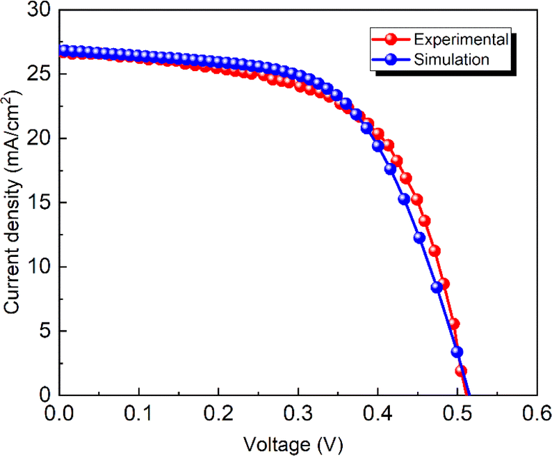
This numerical design is implemented using the SCAPS-1D program, which is reliable simulation software for simulating the behaviours of TFSCs.37 This numerical tool exploits three fundamental semiconductor equations including Poisson's equation, carrier continuity equation, and the electron and hole transport equations to evaluate the electrical and optical features of the PV devices such as energy diagrams, quantum efficiency, current–voltage (I–V), capacitance–voltage (C–V), capacitance–frequency (C–f), and recombination and generation profiles.37 The quasi-Fermi levels as well as electrostatic potential of charge carriers can be calculated using this software. The electric field, carrier concentration, and other solar cell output parameters can also be determined. In the beginning, in order to justify the present simulation approach, the PV outputs of an experimental configuration of Au/Sb2(S,Se)3/CdS/ITO/glass8 are reproduced utilizing the SCAPS-1D program, and the outcomes are compared with the experimental outcomes. The simulation is executed using the different material properties as baseline parameters that are described in the prior studies and are listed in Tables 1 and 2. The experimental and simulation J–V characteristics are demonstrated in Fig. 1. Additionally, the output parameters obtained in both cases are reported in Table 3. It can be recognized from the outcomes that the SC outputs of the simulation studies are approximately indifferent to the experimental results. Therefore, a complete similarity is attained between the experimental and simulation studies. This outstanding steadiness between the experimental and simulation work validates the accuracy of this numerical approach.
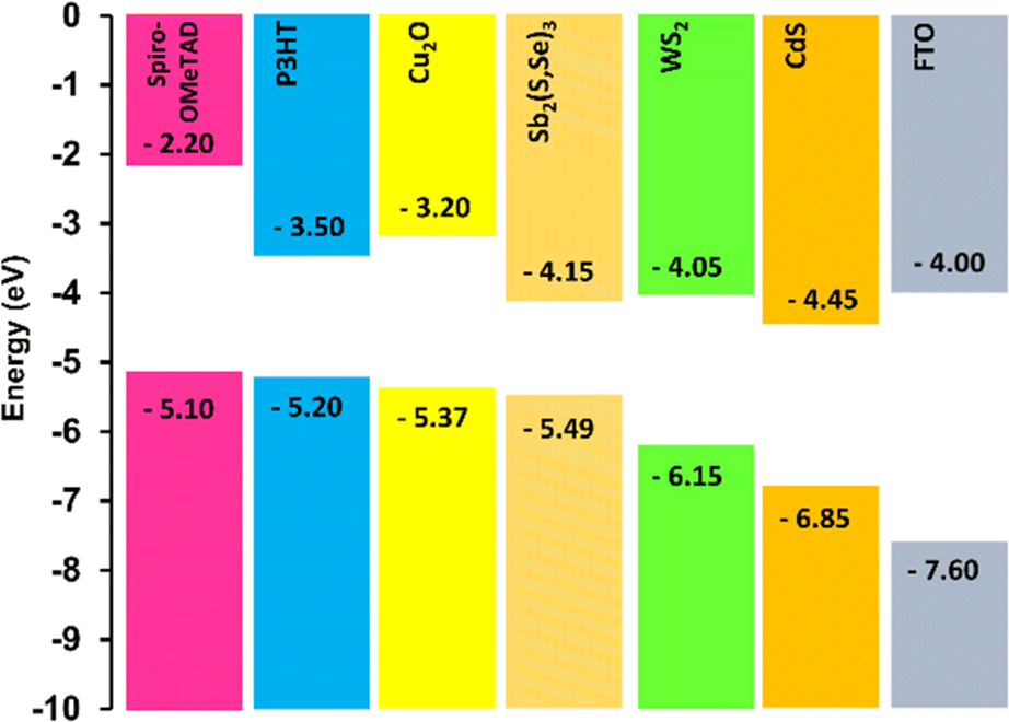
Table 1 Baseline parameters used for different layers in Sb2(S,Se)3-based TFSC8,15,16,25,29,38–42
| Parameters (unit) |
n+-type window (FTO) |
n-type buffer (CdS) |
n-type buffer (WS2) |
p-type absorber Sb2(S, Se)3 |
p+-type HTL (Cu2O) |
p+-type HTL (P3HT) |
p+-type HTL (Spiro-OMeTAD) |
| Variable. |
| Thickness (μm) |
0.05 |
0.05 |
0.05 |
1.0a |
0.1 |
0.1 |
0.1 |
| Band gap (eV) |
3.6 |
2.4 |
2.1 |
1.34 |
2.17 |
1.70 |
2.9 |
| Electron affinity (eV) |
4 |
4.45 |
4.05 |
4.15 |
3.20 |
3.5 |
2.2 |
| Dielectric permittivity (relative) |
9 |
9 |
13.6 |
15 |
7.11 |
3 |
3 |
| CB effective DOS (cm−3) |
2.2 × 10¹⁸ |
2.2 × 10¹⁸ |
2.0 × 10¹⁸ |
1018 |
2.0 × 10¹⁷ |
2.0 × 10²¹ |
2.5 × 10²⁰ |
| VB effective DOS (cm−3) |
1.8 × 10¹⁹ |
1.8 × 10¹⁹ |
2.0 × 10¹⁸ |
1020 |
1.1 × 10¹⁹ |
2.0 × 10²¹ |
2.5 × 10²⁰ |
| Electron mobility (cm2 V−1 s−1) |
100 |
100 |
100 |
10 |
200 |
1.8 × 10⁻³ |
2.0 × 10⁻⁴ |
| Hole mobility (cm2 V−1 s−1) |
25 |
25 |
100 |
1 |
80 |
1.86 × 10⁻² |
2.0 × 10⁻⁴ |
| Donor density ND (cm−3) |
1018 |
1018 |
1018 |
0 |
0 |
0 |
0 |
| Acceptor density NA (cm−3) |
0 |
0 |
0 |
2.50 × 10¹⁷a |
1018 |
1018 |
1018 |
| Defect density (cm−3) |
|
1014 |
1014 |
1014a |
1015 |
1015 |
1015 |
Table 2 Defect parameters at absorber/ETL and HTL/absorber interfaces
| Parameters (unit) |
Sb2(S,Se)3/WS2 interface |
Cu2O/Sb2(S,Se)3 interface |
| Defect type |
Neutral |
Neutral |
| Capture cross-section of electrons (cm2) |
10−19 |
10−19 |
| Capture cross-section of holes (cm2) |
10−19 |
10−19 |
| Reference for defect energy level Et |
Above the highest Ev |
Above the highest Ev |
| Energy with respect to reference (eV) |
0.6 |
0.6 |
| Total density (cm−2) |
1010 |
1010 |
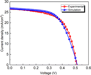 |
| | Fig. 1 Illustration of J–V curve of experimental and simulated outcomes attained for the Sb2(S,Se)3 solar cell architecture. | |
Table 3 Similarity between experimental and simulated outputs of Sb2(S,Se)3 TFSCs
| Research area |
Voc (V) |
Jsc (mA cm−2) |
FF (%) |
PCE (%) |
| Experimental8 |
0.515 |
26.80 |
59.10 |
8.17 |
| Simulation |
0.516 |
26.84 |
59.10 |
8.18 |
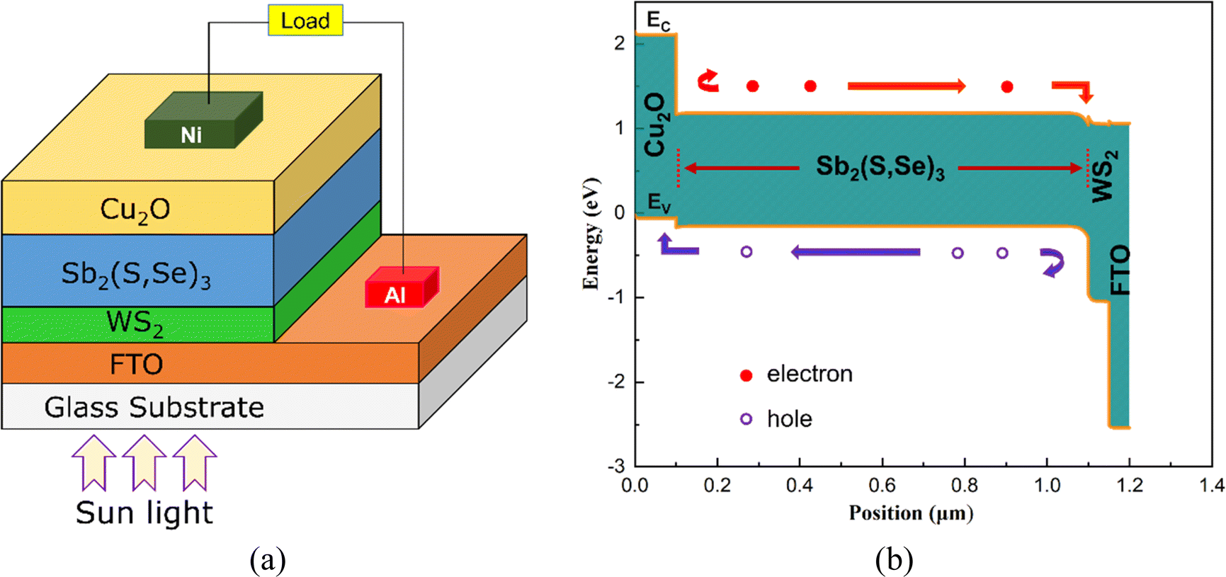
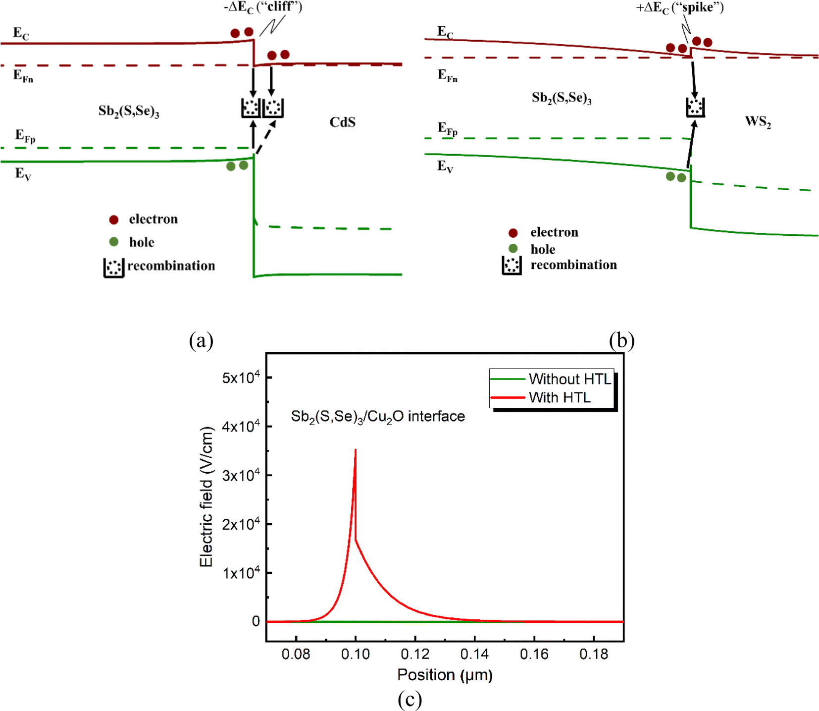
After confirming the reliability of utilizing the SCAPS-1D simulator, we have designed the experimental PV structure to Ni/Cu2O/Sb2(S,Se)3/WS2/FTO/Al. Fig. 2(a) depicts the schematic arrangement of the proposed heterojunction Ni/Cu2O/Sb2(S,Se)3/WS2/FTO/Al TFSC configuration. The optimum thicknesses of Sb2(S,Se)3 absorber layer, p+ type Cu2O HTL, and n-type WS2 ETL are selected to be 1.0 μm, 0.1 μm, and 0.05 μm, respectively. Additionally, a 0.05 μm-thick FTO serves as the window layer. Fig. 2(b) depicts the energy band illustration of the designed TFSC architecture (Ni/Cu2O/Sb2(S,Se)3/WS2/FTO/Al). It can be noticed in Fig. 2(b) that the Cu2O HTL has a larger conduction band (CB) than the Sb2(S,Se)3 absorber, with a CB offset (CBO) value of 0.95 eV at the HTL/absorber junction, which contributes to the transportation of photo-induced electrons towards the rear electrode.24 Additionally, the valence band offset (VBO) of HTL closely aligns with that of the active layer, resulting in a VBO of 0.12 eV at the Cu2O/Sb2(S,Se)3 junction. This low barrier facilitates efficient conduction of photo-induced holes across the Cu2O HTL from the absorber to the rear metallic electrode.24 Consequently, the effective junction development between the Cu2O HTL and the Sb2(S,Se)3 absorber not only blocks the flow of photo-generated minority charge carriers (electrons) toward the rear electrode but also enhances the overall PV performance significantly by facilitating the conduction of holes from the active layer to the back electrode through the HTL.
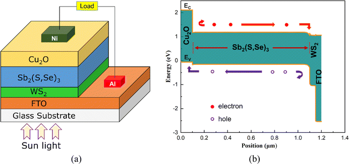 |
| | Fig. 2 (a) Schematic and (b) energy band illustrations of proposed heterostructure Ni/Cu2O/Sb2(S,Se)3/WS2/FTO/Al solar device. | |
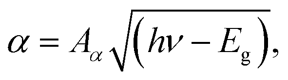
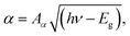
Fig. 3 represents the energy level illustration of the suggested SC architecture featuring numerous and ETLs and HTLs. It is evident that a relatively modest VBO at the Cu2O/Sb2(S,Se)3 interface facilitates smooth hole transportation from the absorber to the rear contact across the HTL. Sufficient built-in voltage at the HTL/absorber junction is ensured. This minimizes minority carrier recombination loss by impeding the electron flow from the absorber to rear contact. The proposed solar device operates under AM 1.5G light spectrum at 300 K temperature with solar irradiance of 100 mW cm−2. The accuracy of performance is obtained through simulation relies on the careful selection of material baseline parameters for each layer of the device. These parameters along with interfacial conditions are summarized in Tables 1 and 2, respectively. All values are meticulously compiled from several published experimental and numerical researches.8,15,16,25,29,38–42 The electron and hole thermal velocity are maintained approximately uniform at 107 cm s−1.43 A neutral type bulk defect with Gaussian energetic distribution is adopted for all layers.27 The absorption coefficient (α) for each layer of the proposed structure is determined using the specified equations44,45
| |
 | (1) |
where
Eg is the energy band gap,
hv is the incident photon energy, and the pre-factor
Aα is chosen to be 10
5 cm
−1eV
−1/2 for all the materials exploited in the proposed heterojunction. Without requiring a substantial financial investment or intricate fabrication processes, this numerical simulation precisely determines the operation of the device and forecasts the impact of its baseline parameters on the functioning and performance of the proposed TFSC.
 |
| | Fig. 3 Energy level representation of proposed heterostructure TFSC. | |
2.2. Artificial neural network
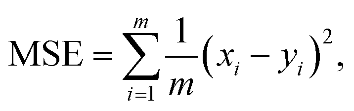
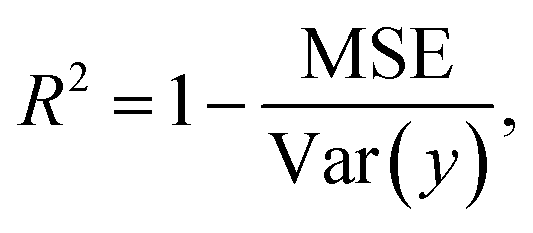
An artificial neural network (ANN) method based on machine learning (ML) can be employed to estimate the outputs of the SC systems. Nowadays, ML is employed to predict the characteristics and functionalities of PV devices through the analysis of a substantial and reliable dataset derived from numerous experimental and simulation outcomes. The working flow of the ML algorithm is demonstrated in Fig. 4. Among the various ML algorithm, random forest tree, decision tree, Bayesian network, regression analysis, supporting vector machine, genetic algorithm, and ANN are commonly employed.46,47 A method for supervised ML that predicts the correlation between the anticipated and true value is called the linear regression algorithm (LRA). The primary benefits of LRA are simple and computationally less expensive.48 This algorithm can be utilized to forecast the output characteristics of TFSC. To relate the actual value with the predicted value, a goodness-of-fit straight line can be employed, which is indicated by the following equation.49where x, y, z, β represents the actual value, predicted value, slope intercept, and the regression coefficient, correspondingly. Study reports that, for a reliable ML algorithm, the minimum number of samples in a dataset needed is 50, though it may vary depending on the type of model used.50 The accuracy of the ML algorithm can be evaluated by assessing the root mean square error (RMSE) and coefficient of determination (R2).49 The RMSE and R2 can be indicated by the following equations,50| |
 | (3) |
| |
 | (4) |
| |
 | (5) |
where xi and yi represents the predicted and target variable of the model whether the variance of the sample data is expressed by Var(y).
 |
| | Fig. 4 Working flow of machine learning. | |
3. Results and discussion
3.1. Enlargement of PV performances of Sb2(S,Se)3 solar cell
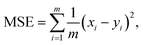
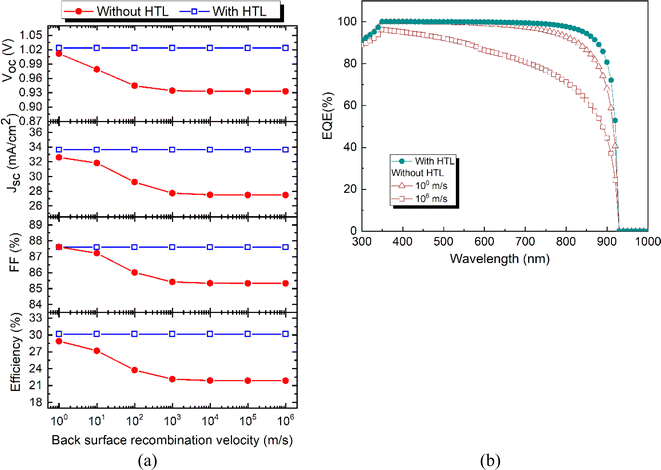
The J–V characteristics of the designed TFSCs featuring various ETLs and HTLs are illustrated in Fig. 5(a). The performance parameters of Sb2(S,Se)3 PV device structures with several ETLs and HTLs and their corresponding VBO and CBO values are also listed in Table 4. In Fig. 5(a), it is evident that Sb2(S,Se)3-based TFSCs with HTLs exhibit superior J–V characteristics compared to those without HTL. The high carrier recombination loss at the rear surface of heterostructure TFSC is the reason for the lesser device outputs of the cell without HTL. Owing to the toxicity associated with cadmium, our research demonstrates that Sb2(S,Se)3-based PV devices with WS2 ETL offer slightly superior outcomes than those with CdS ETL. Specifically, a PCE of 21.87% is attained for the WS2 ETL-based Sb2(S,Se)3 TFSC, while the PV cell with CdS ETL attains the PCE of 19.97%. This efficiency improvement may be associated with reduced charge recombination loss at the front side. Table 4 also indicates that the Sb2(S,Se)3-based PV device employing Cu2O HTL exhibit superior performance compared to the PV structures with Spiro-OMeTAD and P3HT HTLs. For instance, the optimized Ni/Cu2O/Sb2(S,Se)3/WS2/FTO/Al SC configuration accomplish a Voc of 1.02 V, Jsc of 33.65 mA cm−2, FF of 87.59%, and efficiency of 30.18%. Conversely, the slightly larger VBOs calculated at the P3HT/Sb2(S,Se)3 and Spiro-OMeTAD/Sb2(S,Se)3 interfaces may restrict the flow of hole from the absorber to the rear electrode. Therefore, the lower conversion efficiencies of Sb2(S,Se)3 devices with P3HT and Spiro-OMeTAD HTLs are caused by the higher carrier recombination loss at the back surface.25 Therefore, employing the Cu2O as HTL yields better device performances regarding Voc and Jsc (as demonstrated in J–V analysis).
 |
| | Fig. 5 (a) J–V characteristics and (b) EQE curves as a function of wavelength of Sb2(S,Se)3-based SCs without and with HTLs. | |
Table 4 PV parameters of Sb2(S,Se)3 PV device structures with different ETLs and HTLs along with VBO and CBO values
| Configurations |
CBO (eV) |
VBO (eV) |
Voc (V) |
Jsc (mA cm−2) |
FF (%) |
Efficiency (%) |
| Al/FTO/CdS/Sb2(S,Se)3/Ni |
−0.30 |
|
0.93 |
25.85 |
83.01 |
19.97 |
| Al/FTO/WS2/Sb2(S,Se)3/Ni |
0.10 |
|
0.93 |
27.48 |
85.33 |
21.87 |
| Al/FTO/WS2/Sb2(S,Se)3/Spiro-OMeTAD/Ni |
1.95 |
0.39 |
0.99 |
30.94 |
83.84 |
25.77 |
| Al/FTO/WS2/Sb2(S,Se)3/P3HT/Ni |
0.65 |
0.29 |
1.01 |
32.24 |
85.98 |
27.99 |
| Al/FTO/WS2/Sb2(S,Se)3/Cu2O/Ni |
0.95 |
0.12 |
1.02 |
33.65 |
87.59 |
30.18 |
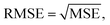
Fig. 5(b) also illustrates the external quantum efficiency (EQE) curves as a function of wavelength for Sb2(S,Se)3-based TFSCs with and without HTLs. The EQE expresses the amount of charge carriers that a PV device can accumulate from irradiance photons of certain energy.20 The enhanced EQE of proposed Sb2(S,Se)3 TFSC with Cu2O HTL at the wavelengths of 400 to 800 nm is observed in the figure. This happens as a result of the back-surface field established by the Cu2O HTL because of the sufficient accumulation of charge carriers from the Sb2(S,Se)3 layer. The graph demonstrates that the QE diminishes to zero when the wavelength exceeds 930 nm. On account of the lower energy below Eg of the Sb2(S,Se)3 layer, the incident light cannot be absorbed by active layer. Hence, the optimum EQE could be achieved from the proposed PV device with WS2 ETL and Cu2O HTL at wavelengths between 400 nm and 800 nm.
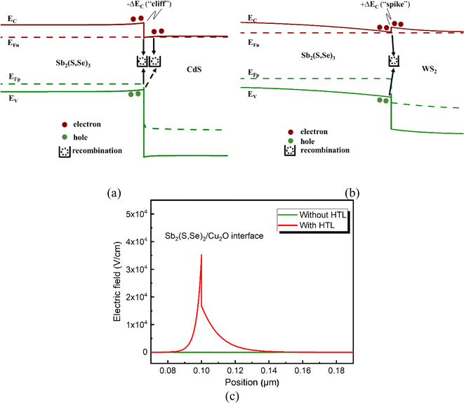
The energy band illustration of the proposed SC with CBO values of −0.30 eV at the Sb2(S,Se)3/CdS interface and +0.10 eV at the Sb2(S,Se)3/WS2 interface are depicted in Fig. 6(a) and (b). Due to the higher CB energy of the Sb2(S,Se)3 layer compared to the CdS ETL, a negative ‘cliff-like’ band orientation is formed with ΔEc = −0.30 eV. Consequently, electrons–holes recombination at the absorber/ETL interface occurs due to the little band bending which in turn diminishes the performance of the designed TFSC. The activation energy (EA) for minority carrier recombination is determined using Eg of the absorber (Eg.absorber) and the CB offset of the absorber/ETL interfaces, defined as EA = Eg.absorber − |CB offset|.51,52 The minority carrier recombination happens at the interface when EA < Eg.absorber.53–56 The small EA at the Sb2(S,Se)3/CdS junction results in a small hole barrier, leading to carrier recombination at both the absorber material surface and the junction between the absorber and ETL.53,57 The accelerated charge recombination at the absorber surface and the absorber/ETL interface is shown by solid and dashed arrows, respectively, and are depicted in the Fig. 6(a). Besides, the energy band diagrams of Sb2(S,Se)3/WS2 interface is depicted in Fig. 6(b). It is evident from the illustration that the CB of the WS2 ETL is positioned above the absorber layer. This generates a positive ‘spike-like’ band alignment with CBO values of ΔEc = +0.10 eV. For spike-like band structure, EA > Eg.absorber and this large EA at the Sb2(S,Se)3/WS2 interface causes elevated hole barrier. This uplifted band bending at the interface blocks the hole transportation to the interface and assures the movement of electron from the absorber to the front contact through the ETL. Therefore, the values of Jsc and FF are enhanced which improves the efficiency of the designed TFSC.
 |
| | Fig. 6 Energy band diagrams of TFSCs with CBO values of (a) −0.30 eV at Sb2(S,Se)3/CdS interface and (b) +0.10 eV at Sb2(S,Se)3/WS2 interface and (c) built-in electric field along Sb2(S,Se)3 layer due to formation of p+/p high-low junction. | |
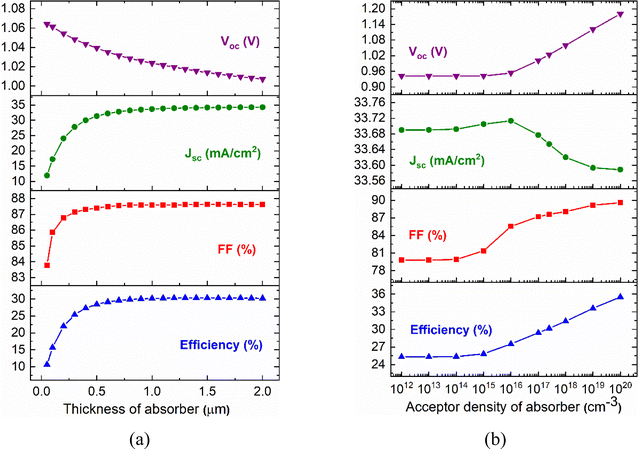
The PV performance can be further intensified by adding an appropriate HTL between the absorber and the back electrode. The VB energy of the HTL should be adjacent to the absorber so that the photo-induced holes can be effectively transferred from the absorber to rear electrode across the HTL.58 For effective hole transfer and electron blocking from the active layer to the back electrode, the values of VBO and CBO at the absorber/HTL junction should be low and high, respectively. A large built-in electric field alongside the absorber can be created ascribed to the establishment of p+/p high-low junction at HTL/Sb2(S,Se)3 interface, as exhibited in Fig. 6(c), which minimizes the carrier recombination loss by preventing the minority electrons at back interface.19,59 Among the three HTLs used in this research, the Cu2O HTL provides low VBO of 0.12 eV which prompts the low energy threshold at the Cu2O/Sb2(S,Se)3 interface for the holes to be conducted.
3.2. Effects of absorber thickness and carrier density on PV performances
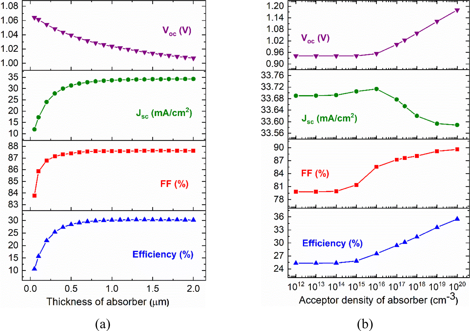
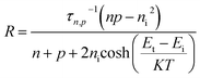
The solar cell's performance parameters are remarkably affected by the thickness and doping densities of the active layer. Fig. 7(a) represents the deviation in the output parameters of the proposed SC structure concerning the Sb2(S,Se)3 absorber's thickness ranging from 0.05 to 2.0 μm. It is evident from Fig. 7(a) that Voc diminishes notably with the rise in absorber layer thickness. This happens due to the enhancement of minority charge carrier's recombination at the thicker absorber.60,61 In this simulation, Voc is achieved to be 1.02 V with an active layer thickness of 1.0 μm. The Jsc enhances substantially with an increase in the thickness up to 1.0 μm and achieves a value of 33.65 mA cm−2, and then it is saturated. Furthermore, the values of FF and PCE increase noticeably with expanding the Sb2(S,Se)3 thickness until 1.0 μm and then is stabilized. This phenomenon occurs due to minority carrier recombination in the active layer before arriving the contacts.62 The proposed Sb2(S,Se)3-based TFSC attains FF of 87.59% and efficiency of 30.18% at 1.0 μm. In this work, by considering the optimum efficiency, materials cost, and light absorption, the thickness of the Sb2(S,Se)3 layer is adjusted to be 1.0 μm for the proposed TFSC.
 |
| | Fig. 7 Variation of Sb2(S,Se)3 absorber's (a) thickness and (b) doping concentration on device output parameters of proposed Ni/Cu2O/Sb2(S,Se)3/WS2/FTO/Al TFSC. | |
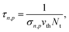
In addition to the thickness, the PV performances are substantially influenced by the acceptor density (NA) of the absorber, as depicted in Fig. 7(b). NA is varied from 1012 to 1020 cm−3. It is seen that Voc enhances with increasing NA. Higher acceptor doping densities result in a lower Fermi energy level of the hole, thus boosting Voc.63 Voc varies from 0.94 to 1.18 V for the deviations of NA from 1012 to 1020 cm−3, individually. Jsc increases slightly and then decreases drastically beyond a doping level of 1016 cm−3, possibly owing to increased recombination of free charge carriers within the absorber.64 Conversely, FF and PCE rise based on the doping concentration of the absorber. FF ranges from 79.79 to 89.60% and PCE from 25.31 to 35.53%, with variations in acceptor concentration from 1012 to 1020 cm−3. Hence, considering the excellent PV performance and production cost, the NA of the proposed device is optimized at 2.50 × 1017 cm3 for the Sb2(S,Se)3 absorber in this research.
3.3. Influences of bulk defect density of absorber on cell performances
The presence of defects in heterojunction PV devices significantly influences the physical and optoelectronic characteristics of the absorber layer making it essential to examine the impact of defect states on the outputs of the designed Sb2(S,Se)3 TFSC. Defects are prevailing at the surfaces and in the bulk. In the p-type active layer, impurity defects are generated by self-doping process.65,66 Consequently, leading to nonradiative electron–hole recombination due to carrier trapping.61 The Shockley–Read–Hall (SRH) model might be utilized to assess the effects of absorber material's bulk defect states on the PV cell outcomes.67,68 From the SRH model, the carrier recombination rate (R) can be stated as| |
 | (6) |
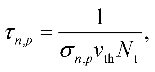
where n and p are the density of electrons, and holes, ni is the intrinsic density, and Ei and Et are the intrinsic energy level and energy level of the trap defects, accordingly. τn,p is the lifetime of charge carriers, which is given by the following equation:| |
 | (7) |
where σn,p indicates the capture cross section of charge carriers; Nt denotes the defect state of the absorber material, and vth stands for the velocity of charge carriers. Since, charge carrier's relaxation time is diminishing with the rise in defect concentration, therefore the recombination rate enhances.
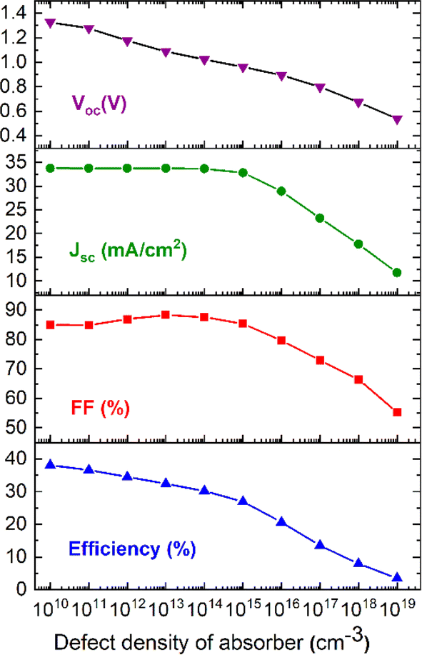
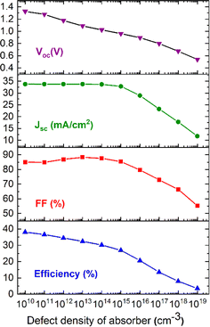
In this theoretical study, we explore the output parameters of the proposed SC by varying the bulk defect level (Nt) of the absorber material between the range of 1010 and 1019 cm−3, as depicted in Fig. 8. The figure reveals a significant fall in Voc as the defect concentration increases, indicating a corresponding rise in recombination rate with high Nt. Specifically, the Voc decreases from 1.33 to 0.54 V with Nt changing from 1010 to 1019 cm−3. Additionally, the Jsc is relatively fixed till Nt of 1014 cm−3 and then it is steadily decreased with further increases in Nt. For instance, the Jsc values are measured at 33.76 mA cm−2 and 11.79 mA cm−2 for defect levels of 1010 and 1019 cm−3, respectively. Conversely, FF notably increases until a defect state of 1013 cm−3 and substantially decreases for high Nt. Specifically, FF values are achieved at 85.01% and 55.31% for Nt of 1010 and 1019 cm−3, respectively. Moreover, the PCE of the proposed TFPV device significantly lessens with increasing the value of Nt. For instance, the efficiency of designed TFSC device is estimated to be 38.06% and 3.52% at defect densities of 1010 and 1019 cm−3, respectively. Therefore, the defect state of the proposed heterojunction Ni/Cu2O/Sb2(S,Se)3/WS2/FTO/Al TFSC is optimized to be 1014 cm−3.
 |
| | Fig. 8 Impacts of absorber defect state on device outcomes of proposed Ni/Cu2O/Sb2(S,Se)3/WS2/FTO/Al architecture. | |
3.4. Effects of interface defects on cell performances
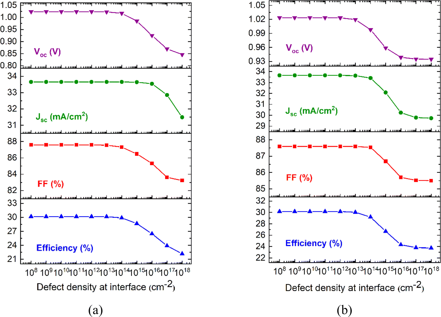
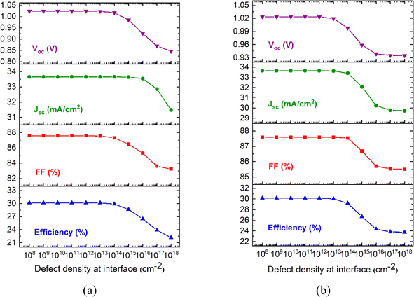
To examine the influence of defect state at the Sb2(S,Se)3/WS2 and Cu2O/Sb2(S,Se)3 interfaces within the Ni/Cu2O/Sb2(S,Se)3/WS2/FTO/Al heterojunction solar cell configuration, an extensive analysis is undertaken, as illustrated in Fig. 9(a) and (b). This analysis calculates critical parameters including Voc, Jsc, FF, and efficiency for the variations of interface defects. Through the manipulation of defect densities ranging from 108 to 1018, initial findings indicate a stable range for the performances within the domain of 108 to 1014. However, surpassing this threshold precipitated a discernible decline in these metrics. This deterioration can be ascribed to the effects of defect level in the Ni/Cu2O/Sb2(S,Se)3/WS2 FTO/Al, wherein defects within the materials or their interfaces act as recombination centers, catalyzing the undesired loss of charge carriers. From Fig. 9(a), it can be identified that Voc is diminished from 1.02 to 0.85 V for the Sb2(S,Se)3/WS2 interface defect level, which differs from 108 to 1018 cm−2 as charge carriers prematurely recombine before reaching the external circuit. Furthermore, the defects restrict passage of charge carriers, culminating in diminished Jsc following the defect concentration of 1016 cm−2. Since the considerable defect concentration at the absorber/buffer interface introduces high series resistance in the heterojunction TFSC, the value of FF is evidently reduced from 87.60% to 83.23% at defect concentrations of 108 and 1018 cm−2, respectively.18 Again, the PCEs of 32.18% and 22.18% are attained for the defect level of 108 and 1018 cm−2, respectively. This happens due to the introduction of asymmetries by defects interrupts the optimal transport and collection of charges, intensifying efficiency losses. Moreover, the defects may trigger parasitic absorption or scattering processes, further attenuating the effective conversion of incident sunlight into electrical energy, thereby diminishing the entire efficiency of the PV cell.
 |
| | Fig. 9 Influences of defect density at (a) Sb2(S,Se)3/WS2 and (b) Cu2O/Sb2(S,Se)3 interfaces on PV parameters of proposed Ni/Cu2O/Sb2(S,Se)3/WS2/FTO/Al structure. | |
The alteration of defects at the Cu2O/Sb2(S,Se)3 interface is varying from 108 to 1018 cm−2 while maintaining the other variables constant, as elucidated in Fig. 9(b). The figure indicates that the cell outputs begin declining beyond the interface defect concentration of 1013 cm−2. The PCE has drastically diminished from 32.18% to 23.76% as a result of defect density rising from 108 to 1018 cm−2, respectively. The reduction in PCE is ascribed to the electron–hole recombination, which results from the greater defect levels at the interfaces.69,70 Therefore, the defect level of 1010 cm−2 is chosen at both interfaces in order to achieve the highest accomplishment of the proposed TFPV device.
3.5. Impacts of temperature and rear contact work function on PV outputs
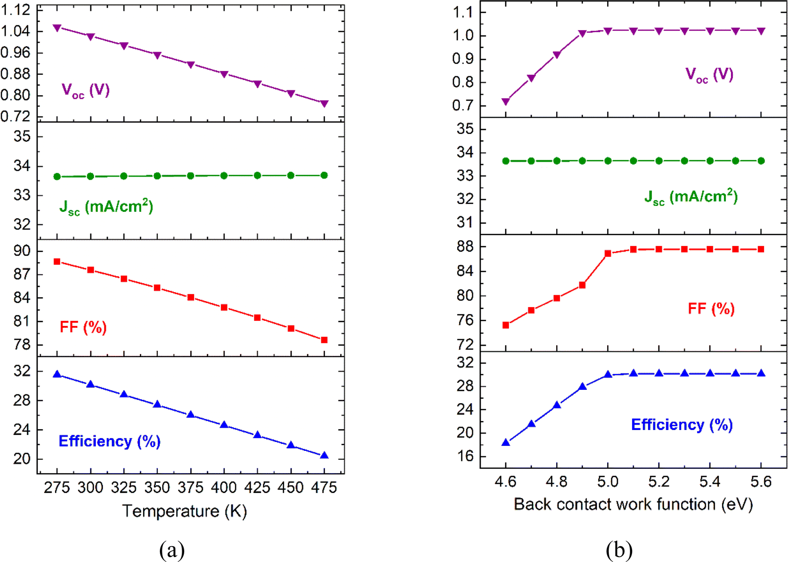
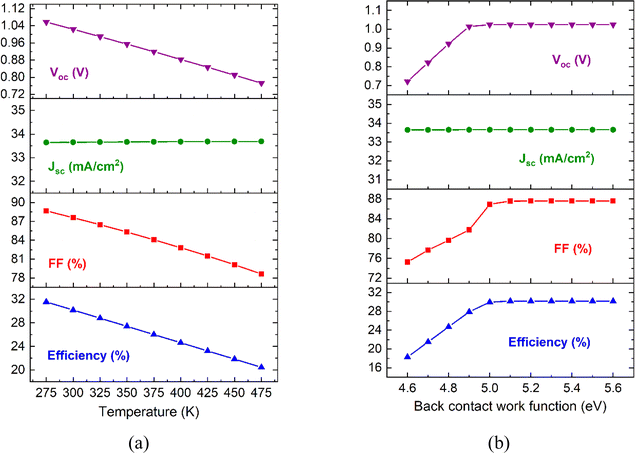
In Fig. 10(a), we have examined the influences of temperature fluctuations on the output parameters of the Ni/Cu2O/Sb2(S,Se)3/WS2/FTO/Al SC. By adjusting the temperature from 275 to 475 K, significant shifts occur in critical performance parameters. Notably, while the Jsc remains relatively consistent across varying temperatures, both the Voc, FF, and PCE display decline. This phenomenon can be elucidated through various mechanisms. Firstly, elevated temperatures induce a broader spread of electron and hole energies within the material, facilitating heightened carrier generation and sustaining Jsc. However, the increased temperature also accelerates carrier recombination rates, leading to reduced Voc and FF due to enhanced non-radiative recombination losses and alterations in charge transfer properties. The combined effect of changes in Voc, Jsc, and FF with temperature influences the PCE of proposed PV cell. However, in this particular case, the reduction in Voc and FF leads to a reduction in PCE, which is measured at 20.47%.
 |
| | Fig. 10 Influences of (a) working temperature and (b) rear electrode work function on output metrics of the proposed Ni/Cu2O/Sb2(S,Se)3/WS2/FTO/Al TFSC. | |
We have also examined the effect of rear contact work function (WF) on the performance of Ni/Cu2O/Sb2(S,Se)3/WS2/FTO/Al TFSC, as demonstrated in Fig. 10(b). By setting the rear contact WF from 4.6 to 5.6 eV, significant shifts in critical performance parameters occur as we obtain constant Jsc, high Voc, FF, and increased PCE. This phenomenon arises due to the crucial role that back contact plays in facilitating accurate charge extraction and carrier transportation throughout the solar cell structure. When the back contact has an optimal working function, it ensures efficient extraction of charges generated inside the device, resulting in a constant Jsc. In addition, proper back contact action promotes proper energy level alignment at the interface, enabling efficient separation of photogenerated electron–hole pairs and thus promoting high Voc. Furthermore, the rear contact WF affects the contact resistance and charge carrier mobility, which contributes to enhanced FF by reducing losses associated with charge transfer and recombination. Thus, these favorable properties combined lead to an increased overall efficiency of 30.18% for the proposed TFSC. It is also manifested in the figure that all the output parameters (except Jsc) increase until the work function reaches ∼5.1 eV and then are unaffected. Therefore, the back-metal contact with a work function >5.1 eV should be preferred to confirm the ohmic contact and attain excellent PV performances. The work function values of 5.35 eV71 for nickel (Ni), 5.47 eV71 for gold (Au), and 5.7 eV71 for platinum (Pt), respectively, have been found. Among them, Au and Pt are rare materials and expensive to fabricate. In contrast, Ni is earth-abundant, highly conductive, easy to manufacture, and cheap, which will make it an appropriate back-contact metal electrode for low-cost solar cell fabrications. In this numerical study, we have employed low-cost Ni as the rear electrode to establish highly efficient and non-toxic Sb2(S,Se)3 TFSC.
3.6. Significance of surface recombination velocity on PV outputs
In this numerical research, the function of back surface recombination velocity (BSRV) on the PV outputs of proposed SC without and with HTL is determined. The BSRV is altered from 1 to 106 m s−1, and the respective outcomes are displayed in Fig. 11(a). From the figure, it is clearly identified that the TFSC with HTL offers excellent performance compared to the TFSC without HTL, and more precisely, the outputs of PV device with HTL are not influenced by the variation of BSRV. This happens because large BSRV eliminates charge carriers by recombination at the rear contact.22 This drawback can be reduced easily by incorporating an HTL between active layer and back contact, since an electric field is generated at p+/p interfaces, which reverses the movement of minority carriers back into the p-type absorber, resulting in an enhanced minority carrier lifespan.60 Since the heterojunction PV device absorbs longer-wavelength photons, increasing the wavelength accelerates recombination at the outer layer.72 The impact of BSRV on the EQE of the designed SC without and with HTL is elucidated in Fig. 11(b). The figure indicates that the EQE of the TFSC without HTL diminishes substantially at long wavelengths due to the extensive recombination at the outermost layer. Therefore, the integration of Cu2O HTL between the absorber and rear contact will eradicate the impact of BSRV by redirecting the movement of minority charges onto the absorber/ETL junction. Hence, the overall performance of the suggested TFPV improves significantly.
 |
| | Fig. 11 (a) PV parameters versus BSRV rate and (b) EQEs as a function of BSRV of Ni/Cu2O/Sb2(S,Se)3/WS2/FTO/Al SCs without and with HTL. | |
3.7. C–V and C–f characteristics of (Sb2(S,Se)3)-based solar cell
Here, to inspect the overall performance of the designed Sb2(S,Se)3 PV device the C–V and C–f studies have been discussed. The built-in potential and doping density of the Sb2(S,Se)3 layer can be derived from the following two equations,73| |
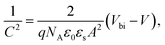 | (8) |
| |
 | (9) |
where A, C, and Vbi are the area of the cell, measured capacitance, and built-in potentials, respectively. Capacitance can be measured by varying the applied voltage, which can be further used to assess the impact of an AC current on a DC-biased p–n junction.74 The C–V characteristics of the designed TFPV are elucidated in Fig. 12(a) when the frequency was fixed at 1 MHz and voltage changes ranged from −0.8 V to 0.8 V. From the figure, it can be observed that the capacitance increases slightly until the applied potential of 0.2 V is reached and then lifts uniformly. The Mott–Schottky method, which is a function of C and NA, is employed to determine the built-in potential and is illustrated in Fig. 12(a) (inset).75 Fig. 12(b) depicts the C–f features of the proposed SC, and from the figure, it can be discovered that the capacitance changes inversely with respect to the frequency, i.e., the capacitance attains its optimum level at low frequencies and declines at high frequencies. Further, the alteration of the conductance–frequency (G–f) characteristics is illustrated in Fig. 12(b) (inset) and it is seen that the conductance of the designed SC is low at the lower frequency and high at the higher frequency, i.e., the G–f curve shows the opposite behavior of the C–f curve.
 |
| | Fig. 12 (a) C–V and (b) C–f characteristics of Ni/Cu2O/Sb2(S,Se)3/WS2/FTO/Al solar cell. | |
3.8. Cell characteristics through ANN
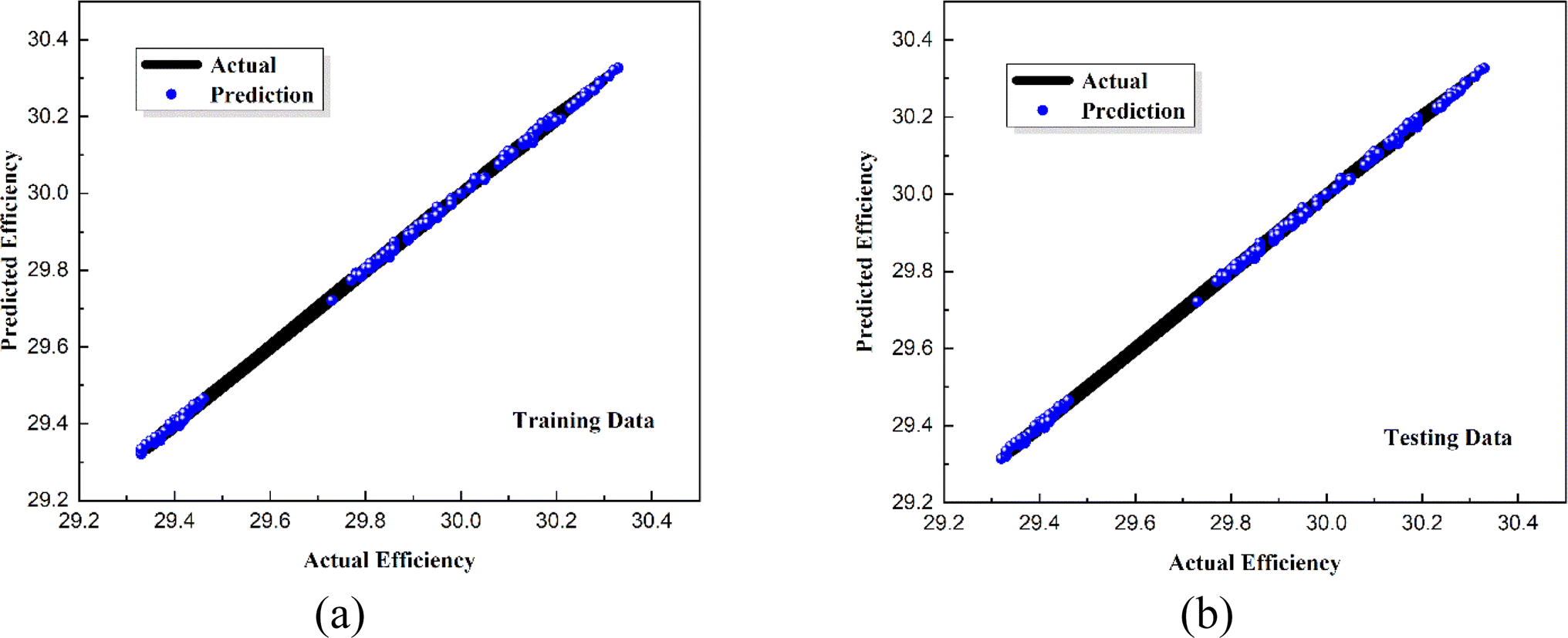
In this study, Neural Designer ML software is employed to build ANN models that forecast the performance of the suggested TFSC without having the programming knowledge. The SCAPS-1D simulator is employed to prepare the initial datasets. The samples in the dataset are categorized into training, selection, and testing. Table 5 shows the dataset used in this model. In this research, the number of samples used is 1024. Among them, 616 (60.2%), 204 (19.9%), and 204 (19.9%) samples are used for training, selection, and testing the model, respectively. The goodness-of-fit regression plot for the predicted PCE versus the actual PCE for both training and testing data are demonstrated in Fig. 13(a) and (b). The coefficient of determination (R2) is a commonly employed measure of goodness-of-fit metrics, which implies that, in the case of perfect fit, the value of R2 would be 1. Subsequently, the best possible performance of the ANN model may be identified for the training, selection, and testing data when the lowest values of MSE, and RMSE are attained. The error metrics of the ANN model are listed in Table 6.
Table 5 A statistical overview of dataset utilized to train ANN model
| Samples |
Thickness |
Bandgap |
Electron affinity |
Electron mobility |
Hole mobility |
Efficiency |
| 1 |
0.95 |
1.25 |
4.1 |
6 |
0.8 |
29.32 |
| 2 |
0.95 |
1.25 |
4.1 |
6 |
1 |
29.32 |
| — |
— |
— |
— |
— |
— |
— |
| 1024 |
1.1 |
1.4 |
4.25 |
12 |
1.4 |
30.03 |
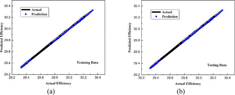 |
| | Fig. 13 Correlation graphs of ANN predicted versus actual PCE for (a) training and (b) testing data for proposed Ni/Cu2O/Sb2(S,Se)3/WS2/FTO/Al TFSC. | |
Table 6 An overview of ANN model's effectiveness
| Performance metric |
Training |
Selection |
Testing |
| Mean squared error |
0 |
0.001 |
0.001 |
| Root mean squared error |
0.02 |
0.026 |
0.024 |
| Determination, R2 |
0.999337 |
0.999342 |
0.999345 |
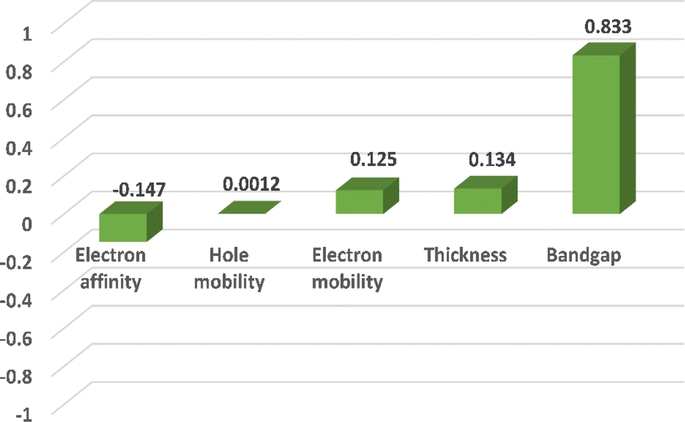
The Pearson Correlation Coefficients (PCCs) are a linear correlation technique used to analyze the interdependencies between features and target variables in a ML model.76–78 The Pearson correlation chart is shown in Fig. 14, where correlations adjacent to 0 indicate no relationship between the variables, and correlations near −1 or 1 indicate the strength and direction of the correlation between the feature and desired variables. From the figure, it can be seen that, out of the five features, the bandgap has the most substantial significance. There are a number of techniques, such as partial derivatives, Lek's profile method, Garson's algorithm, the connection weights algorithm, etc., to determine which input variables have the most influence on the model predictions.79 To ascertain the significance of the input variables, this present research uses partial derivatives of the output variables according to the inputs. The influence of input variables on the target variable is depicted in Fig. 15, where positive signs imply a direct relationship, negative signs denote a reverse relationship, and near-zero output indicates no impact of input variable changes. A near-zero output indicates no impact of input variable changes. From the figure, it can be observed that the three leading inputs for this model are band gap, electron affinity, and thickness, which have values of −0.366, −0.31, and 0.209, respectively.
 |
| | Fig. 14 Pearson correlations chart. | |
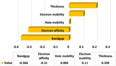 |
| | Fig. 15 Impact of input parameters on PCE. | |
3.9. Overall PV outputs of optimized Sb2(S,Se)3-based TFSC
In this numerical research, the physical parameters of the distinct layers have been optimized and utilized in the heterojunction Ni/Cu2O/Sb2(S,Se)3/WS2/FTO/Al TFSC, which are displayed in Table 7. To design and develop the extremely efficient Sb2(S,Se)3 TFSC, these preferable intrinsic parameters will be beneficial for the researchers of solar energy systems. The experimental and numerical outcomes achieved for the Sb2(S,Se)3-based TFSCs are compared in Table 8. An impressive PCE of 30.18% along Jsc of 33.65 mA cm−2, Voc of 1.02 V, and FF of 87.59% are measured for the designed SC with Cu2O HTL and WS2 ETL. This PV device provides superior performance as compared to those of devices developed in the previous research. This numerical research provides insights into the complexities of solar cells and lays the groundwork for further research in Sb2(SxSe1−x)3-based PV devices, paving the way for innovative sustainable energy technology.
Table 7 Various inherent parameters optimized for newly designed Sb2(S,Se)3 PV cell
| Optimized parameters (unit) |
WS2 ETL |
Sb2(S,Se)3 absorber |
Cu2O HTL |
Interface defect density |
| Sb2(S,Se)3/WS2 |
Cu2O/Sb2(S,Se)3 |
| Thickness (μm) |
0.05 |
1.0 |
0.1 |
— |
— |
| ND (cm−3) |
1018 |
— |
— |
— |
— |
| NA (cm−3) |
— |
2.50 × 10¹⁷ |
1018 |
— |
— |
| Nt (cm−3) |
1014 |
1014 |
1015 |
— |
— |
| σn,p (cm2) |
— |
— |
— |
10−19 |
10−19 |
| Total density (cm−2) |
— |
— |
— |
1010 |
1010 |
Table 8 Comparison of efficiencies assessed experimentally and numerically for Sb2(S,Se)3-based TFSCs
| Configurations |
Types of research |
Efficiency (%) |
Ref. |
| ITO/CdS/Sb2(S,Se)3/Au |
Experimental |
8.17 |
8 |
| FTO/CdS/Sb2(S,Se)3/Spiro-OMeTAD/Au |
” |
10.5 |
11 |
| FTO/Zn(O,S)/CdS/Sb2(S,Se)3/Spiro-OMeTAD/Au |
” |
10.7 |
80 |
| ITO/CdS/Sb2(S,Se)3/MnS-HTL/Au |
Theoretical |
12.7 |
81 |
| ITO/CdS/Sb2(S,Se)3/Au |
” |
14.86 |
14 |
| ITO/CdS/Sb2(S,Se)3/MoS2/Mo |
” |
25.67 |
15 |
| FTO/WS2/Sb2(S,Se)3/Cu2O/Ni |
” |
30.18 |
This work |
The performance of solar cells depends on their design, material properties, and fabrication technology. Note that there are crucial production conditions that have to be considered to develop highly efficient Sb2(S,Se)3 solar cells. A suitable deposition method realizes excellent morphology and crystallinity of films fabricated for heterojunction solar devices. Nonetheless, defect states in bulk materials as well as at interfaces or recombination centers, leading to the device's poor stability and performance. Therefore, to achieve long-term stability and high performance, various kinds of defects, energy band alignment, and non-radiative recombination should be resolved through the incorporation of defect less bulk absorber layer, ETL, and HTL, as well as defect less interfaces in the heterojunction PV system. In this work, a theory to explain the phenomenon of enhancing the overall performance of Sb2(S,Se)3 solar cells is developed. The outcomes derived from the presented theory can be compared with practical investigations. Experimental study is essential within science for deciding the usefulness of offered theories and approaches. To validate an experimental study and the proposed method, further research on the fabrication of Sb2(S,Se)3 solar cells would be required. Moreover, further investigation describing models or assumptions related to the oxidation of Cu2O HTL and its impact on the charge transport layer will be needed in our future work.
4. Conclusions
Herein, we have employed the SCAPS-1D simulator to design a novel heterojunction TFSC configuration, namely Ni/Cu2O/Sb2(S,Se)3/WS2/FTO/Al and thoroughly investigated its optoelectronic properties. Our approach aims at enhancing the PV performance of the suggested device by using WS2 as an ETL instead of the conventional toxic CdS in Sb2(S,Se)3-based SCs. Additionally, several HTLs including Spiro-OMeTAD, P3HT, and Cu2O are introduced in this research to identify the optimal PV performances. Our findings reveal that the Cu2O emerges as the most effective HTL material for the Sb2(S,Se)3 TFSC, significantly enhancing the device's performances by mitigating carrier recombination loss at the heterojunction structure's back surface. Furthermore, we have evaluated the effects of various factors including thickness, defect concentration, bulk defects, interface defects, operating temperature, and series and shunt resistances on the outcomes of the suggested TFSC. We have determined the optimal thicknesses of the FTO window, WS2 ETL, Sb2(S,Se)3 absorber, and Cu2O HTL to be 0.05, 0.05, 1.0, and 0.1 μm, respectively, by optimization procedures. Moreover, the acceptor concentration and defect densities for the Sb2(S,Se)3 layer are optimized at 2.5 × 10¹⁷ and 1014 cm−3, respectively. Our investigation yields promising outputs for the proposed PV structure, achieving Voc, Jsc, FF, and efficiency of 1.02 V, 33.65 mA cm−2, 87.59%, and 30.18%, respectively. Finally, the machine learning algorithm is utilized to assess the impact of different input parameters on the behavior of the proposed PV device. Notably, the parameters including bandgap, electron affinity, and thickness of Sb2(S,Se)3 layer are identified as highly influential. Furthermore, thats study reveals that the predicted PCE closely matched the actual PCE for both training and testing data sets. It is expected that the presented results will provide crucial insights for scientists to develop extremely efficient, economical, and cadmium-free non-toxic heterojunction Sb2(S,Se)3 TFSCs.
Data availability
The data that support the findings of this study are available from the corresponding author upon reasonable request.
Conflicts of interest
The authors have no conflicts of interest.
Acknowledgements
We are thankful to Dr Marc Burgelman from the University of Gent in Belgium for supplying the SCAPS-1D modeling program.
References
- Y. C. Choi, Y. H. Lee, S. H. Im, J. H. Noh, T. N. Mandal, W. S. Yang and S. I. Seok, Adv. Energy Mater., 2014, 4, 1301680 CrossRef.
- L. Yao, L. Lin, H. Liu, F. Wu, J. Li, S. Chen, Z. Huang and G. Chen, J. Mater. Sci. Technol., 2020, 58, 130–137 CrossRef CAS.
- X. Wang, R. Tang, C. Wu, C. Zhu and T. Chen, J. Energy Chem., 2018, 27, 713–721 CrossRef.
- K. Li, R. Kondrotas, C. Chen, S. Lu, X. Wen, D. Li, J. Luo, Y. Zhao and J. Tang, Sol. Energy, 2018, 167, 10–17 CrossRef CAS.
- W. Wang, X. Wang, G. Chen, L. Yao, X. Huang, T. Chen, C. Zhu, S. Chen, Z. Huang and Y. Zhang, Adv. Electron. Mater., 2019, 5, 1800683 CrossRef.
- Y. Lu, K. Li, X. Yang, S. Lu, S. Li, J. Zheng, L. Fu, C. Chen and J. Tang, ACS Appl. Mater. Interfaces, 2021, 13, 46858–46865 CrossRef CAS.
- Y. Pan, D. Zheng, J. Chen, J. Zhou, R. Wang, X. Pan, X. Hu, S. Chen, P. Yang and J. Tao, J. Alloys Compd., 2022, 906, 164320 CrossRef CAS.
- Y. Pan, X. Hu, Y. Guo, X. Pan, F. Zhao, G. Weng, J. Tao, C. Zhao, J. Jiang and S. Chen, Adv. Funct. Mater., 2021, 31, 2101476 CrossRef CAS.
- S. Rijal, A. Adhikari, R. A. Awni, C. Xiao, D.-B. Li, B. Dokken, A. Ellingson, E. Flores, S. S. Bista and D. Pokhrel, Sol. RRL, 2023, 7, 2201009 CrossRef CAS.
- J. Li, Y. Zhao, C. Li, S. Wang, X. Chen, J. Gong, X. Wang and X. Xiao, Adv. Sci., 2022, 9, 2202356 CrossRef CAS PubMed.
- X. Wang, R. Tang, C. Jiang, W. Lian, H. Ju, G. Jiang, Z. Li, C. Zhu and T. Chen, Adv. Energy Mater., 2020, 10, 2002341 CrossRef CAS.
- S. Huang, Y. Xing, H. Zhu, T. Zhang, K. Geng, Y. Yang, H. Zhang, Q. Gu, J. Qiu and S. Jiang, J. Mater. Chem. C, 2024, 12, 3098–3104 RSC.
- X. Ni, J. Liu, F. Xu, J. Zhang, S. Jiang, B. Fang, H. Guo, N. Yuan, J. Ding and S. Zhang, Chem. Eng. J., 2024, 490, 151574 CrossRef CAS.
- M. S. Salem, A. Shaker, T. S. Almurayziq and M. T. Alshammari, Sol. Energy Mater. Sol. Cells, 2022, 248, 112001 CrossRef CAS.
- R. Kumar, R. Kumari, K. Maurya and V. Singh, Mater. Today Sustain., 2022, 20, 100218 Search PubMed.
- T. M. Khan, A. Hosen, O. Saidani and S. R. Al Ahmed, Mater. Today Commun., 2024, 40, 109639 CrossRef CAS.
- S. Rühle, Sol. Energy, 2016, 130, 139–147 CrossRef.
- S. R. Al Ahmed, A. Sunny and S. Rahman, Sol. Energy Mater. Sol. Cells, 2021, 221, 110919 CrossRef.
- M. A. Rahman, Sol. Energy, 2021, 215, 64–76 CrossRef.
- A. Hosen, S. Yeasmin, K. S. B. Rahmotullah, M. F. Rahman and S. R. Al Ahmed, Opt. Laser Technol., 2024, 169, 110073 CrossRef CAS.
- A. Hosen, M. S. Mian and S. R. A. Ahmed, Adv. Theory Simul., 2023, 6, 2200652 CrossRef CAS.
- S. R. A. Ahmed, Energy Fuels, 2023, 38, 1462–1476 CrossRef.
- S. R. Al Ahmed, M. Rahaman, A. Sunny, S. Rahman, M. S. Islam, T. A. E.-M. Taha, Z. Alrowaili and M. S. Mian, Opt. Laser Technol., 2023, 159, 108942 CrossRef.
- Y. Cao, X. Zhu, H. Chen, X. Zhang, J. Zhouc, Z. Hu and J. Pang, Sol. Energy Mater. Sol. Cells, 2019, 200, 109945 CrossRef CAS.
- M. N. H. Riyad, A. Sunny, M. M. Khatun, S. Rahman and S. R. A. Ahmed, Eng. Rep., 2023, 5, e12600 CrossRef CAS.
- J. Al Mahmud, M. F. Rahman, A. Kuddus, M. H. Ali, A. S. Islam, M. D. Haque, S. R. Al Ahmed, M. Mushtaq and A. B. M. Ismail, Energy Adv., 2023, 2, 1843–1858 RSC.
- M. M. Khatun, A. Hosen and S. R. Al Ahmed, Heliyon, 2023, 9, e20603 CrossRef CAS PubMed.
- T. M. Khan and S. R. A. Ahmed, Adv. Theory Simul., 2024, 2400353 CrossRef.
- P. Sawicka-Chudy, M. Sibiński, G. Wisz, E. Rybak-Wilusz and M. Cholewa, J. Phys.: Conf. Ser., 2018, 1033, 012002 CrossRef.
- M. Shasti and A. Mortezaali, Phys. Status Solidi A, 2019, 216, 1900337 CrossRef.
- Y. Liu, X. Tan, J. Liang, H. Han, P. Xiang and W. Yan, Adv. Funct. Mater., 2023, 33, 2214271 CrossRef CAS.
- A. Mellit and S. Kalogirou, in Artificial Intelligence for Smart Photovoltaic Technologies, AIP Publishing LLC Melville, New York, 2022, pp. 1–20 Search PubMed.
- N. Ghalambaz, J. Ganji and P. Shabani, J. Comput. Electron., 2021, 20, 966–973 CrossRef CAS.
- S. Kim, Y. Jeong, D.-W. Han and C. B. Mo, J. Electron. Mater., 2023, 52, 1–11 CrossRef.
- F. Li, X. Peng, Z. Wang, Y. Zhou, Y. Wu, M. Jiang and M. Xu, Energy Environ. Mater., 2019, 2, 280–291 CrossRef.
- M. S. Islam, M. T. Islam, S. Sarker, H. A. Jame, S. S. Nishat, M. R. Jani, A. Rauf, S. Ahsan, K. M. Shorowordi and H. Efstathiadis, ACS Omega, 2022, 7, 22263–22278 CrossRef CAS PubMed.
- M. Burgelman, P. Nollet and S. Degrave, Thin Solid Films, 2000, 361, 527–532 CrossRef.
- K. Sobayel, K. Rahman, M. Karim, M. Aijaz, M. Dar, M. Shar, H. Misran and N. Amin, Chalcogenide Lett., 2018, 15, 307–315 CAS.
- M. K. Hossain, A. Arnab, R. C. Das, K. Hossain, M. Rubel, M. F. Rahman, H. Bencherif, M. Emetere, M. K. Mohammed and R. Pandey, RSC Adv., 2022, 12, 35002–35025 Search PubMed.
- S. Faisal, S. I. Rahman, S. Ahmed and T. I. Dhrubo, IEEE Region 10 Humanitarian Technology Conference (R10-HTC), Dhaka, Bangladesh, 2017, pp. 546–550 Search PubMed.
- A. Das, S. D. Peu, M. A. M. Akanda, M. M. Salah, M. S. Hossain and B. K. Das, Energies, 2023, 16, 2328 CrossRef CAS.
- G. Casas, M. Á. Cappelletti, A. P. Cedola, B. M. Soucase and E. P. y Blancá, Superlattices Microstruct., 2017, 107, 136–143 CrossRef CAS.
- A. Sunny and S. R. A. Ahmed, Phys. Status Solidi B, 2021, 258, 2000630 CrossRef CAS.
- A. Hosen and S. R. Al Ahmed, J. Alloys Compd., 2022, 909, 164823 CrossRef CAS.
- M. S. Islam, S. Rahman, A. Sunny, M. A. Haque, M. S. Mian and S. R. A. Ahmed, Z. Naturforsch. A, 2021, 76, 1045–1059 CrossRef CAS.
- T. Ramesh, U. K. Lilhore, M. Poongodi, S. Simaiya, A. Kaur and M. Hamdi, Malays. J. Comput. Sci., 2022, 132–148 Search PubMed.
- M. Bansal, A. Goyal and A. Choudhary, Decis. Anal. J., 2022, 3, 100071 CrossRef.
- M. M. Salah, Z. Ismail and S. Abdellatif, Mater. Renew. Sustain. Energy, 2023, 12, 187–198 CrossRef.
- N. Kaur, R. Pandey, M. K. Hossain and J. Madan, Sol. Energy, 2023, 264, 112055 CrossRef CAS.
- A. Mahmood and J.-L. Wang, Energy Environ. Sci., 2021, 14, 90–105 RSC.
- L.-L. Wu, G.-W. Wang, J. Tian, D.-M. Wang and D.-L. Wang, Chin. Phys. B, 2022, 31, 108803 CrossRef CAS.
- M. Rahman, Heliyon, 2022, 8, e09800 CrossRef PubMed.
- T. Song, A. Kanevce and J. R. Sites, J. Appl. Phys., 2016, 119, 233104 CrossRef.
- U. Rau and H.-W. Schock, Appl. Phys. A, 1999, 69, 131–147 CrossRef CAS.
- M. Turcu and U. Rau, J. Phys. Chem. Solids, 2003, 64, 1591–1595 CrossRef CAS.
- K. Tanaka, T. Minemoto and H. Takakura, Sol. Energy, 2009, 83, 477–479 CrossRef CAS.
- H. Wilhelm, H.-W. Schock and R. Scheer, J. Appl. Phys., 2011, 109, 084514 CrossRef.
- S. Rahman and S. R. Al Ahmed, Sol. Energy, 2021, 230, 605–617 CrossRef CAS.
- C. Chen, K. Li, S. Chen, L. Wang, S. Lu, Y. Liu, D. Li, H. Song and J. Tang, ACS Energy Lett., 2018, 3, 2335–2341 CrossRef CAS.
- M. M. Khatun, A. Sunny and S. R. Al Ahmed, Sol. Energy, 2021, 224, 956–965 CrossRef CAS.
- M. Lazemi, S. Asgharizadeh and S. Bellucci, Phys. Chem. Chem. Phys., 2018, 20, 25683–25692 RSC.
- A. Sunny, S. Rahman, M. Khatun and S. R. A. Ahmed, AIP Adv., 2021, 11, 065102 CrossRef CAS.
- P. K. Patel, Sci. Rep., 2021, 11, 3082 CrossRef CAS.
- H.-J. Du, W.-C. Wang and J.-Z. Zhu, Chin. Phys. B, 2016, 25, 108802 CrossRef.
- N. K. Noel, S. D. Stranks, A. Abate, C. Wehrenfennig, S. Guarnera, A.-A. Haghighirad, A. Sadhanala, G. E. Eperon, S. K. Pathak and M. B. Johnston, Energy Environ. Sci., 2014, 7, 3061–3068 RSC.
- L. Ma, F. Hao, C. C. Stoumpos, B. T. Phelan, M. R. Wasielewski and M. G. Kanatzidis, J. Am. Chem. Soc., 2016, 138, 14750–14755 CrossRef CAS PubMed.
- S. Z. Haider, H. Anwar and M. Wang, Semicond. Sci. Technol., 2018, 33, 035001 CrossRef.
- L. Lin, L. Jiang, P. Li, B. Fan and Y. Qiu, J. Phys. Chem. Solids, 2019, 124, 205–211 CrossRef CAS.
- J. Tao, X. Hu, J. Xue, Y. Wang, G. Weng, S. Chen, Z. Zhu and J. Chu, Sol. Energy Mater. Sol. Cells, 2019, 197, 1–6 CrossRef CAS.
- Y. Wang, Z. Xia, J. Liang, X. Wang, Y. Liu, C. Liu, S. Zhang and H. Zhou, Semicond. Sci. Technol., 2015, 30, 054004 CrossRef.
- H. B. Michaelson, J. Appl. Phys., 1977, 48, 4729–4733 CrossRef CAS.
- J. L. Gray, Handb. Photovoltaic Sci. Eng., 2011, 2, 82–128 Search PubMed.
- S. T. Ahamed, A. Basak and A. Mondal, Results Opt., 2023, 10, 100364 CrossRef.
- A. Srivastava, S. Tripathy, T. Lenka and V. Goyal, Sol. Energy, 2022, 239, 337–349 CrossRef CAS.
- G. Malliaras, J. Salem, P. Brock and C. Scott, Phys. Rev. B, 1998, 58, R13411 CrossRef CAS.
- S. Kumar and I. Chong, Int. J. Environ. Res. Public Health, 2018, 15, 2907 CrossRef PubMed.
- R. Nematirad and A. Pahwa, IEEE Kansas Power and Energy Conference (KPEC), Manhattan, KS, USA, 2022, pp. 1–4 Search PubMed.
- H. N. Amer, N. Y. Dahlan, A. M. Azmi, M. F. A. Latip, M. S. Onn and A. Tumian, Energy Rep., 2023, 9, 262–266 CrossRef.
- I. O. Oboh, U. H. Offor and N. D. Okon, Energy Rep., 2022, 8, 973–988 CrossRef.
- Y. Zhao, S. Wang, C. Jiang, C. Li, P. Xiao, R. Tang, J. Gong, G. Chen, T. Chen and J. Li, Adv. Energy Mater., 2022, 12, 2103015 CrossRef CAS.
- K. Sekar and S. Mayarambakam, Phys. Status Solidi B, 2023, 260, 2300087 CrossRef CAS.
|
| This journal is © The Royal Society of Chemistry 2024 |
Click here to see how this site uses Cookies. View our privacy policy here. 
 Open Access Article
 This Open Access Article is licensed under a Creative Commons Attribution-Non Commercial 3.0 Unported Licence
 *a
*a