
 Open Access Article
 This Open Access Article is licensed under a Creative Commons Attribution-Non Commercial 3.0 Unported Licence
Bandgap regulation and doping modification of Ga2−xCrxSe3 nanosheets†
Huan Yang ab,
Yue Wuab,
Huirong Liab,
Yiwen Zhangab,
Linmei Gaoab,
Lanfang Wangab and
Fang Wang*ab
ab,
Yue Wuab,
Huirong Liab,
Yiwen Zhangab,
Linmei Gaoab,
Lanfang Wangab and
Fang Wang*ab
aSchool of Chemistry and Materials Science of Shanxi Normal University, Key Laboratory of Magnetic Molecules and Magnetic Information Materials of Ministry of Education, Taiyuan 030032, China. E-mail: wf_0716@163.com
bResearch Institute of Materials Science of Shanxi Normal University, Collaborative Innovation Center for Advanced Permanent Magnetic Materials and Technology of Ministry of Education, Taiyuan 030032, China
First published on 11th June 2024
Abstract
Ga2Se3, an important direct wide bandgap semiconductor with excellent optoelectronic properties, has wide application potential in the fields of photodetectors, photoelectric sensors and solar cells. Herein, we describe the synthesis of Ga2Se3 semiconductor nanoparticles using a high temperature organic liquid phase method. Post-annealing treatment at different temperatures can not only improve the crystallinity of Ga2Se3 nanoparticles, but also regulate its optical band gap ranging from 2.50 to 2.80 eV. We further synthesized Ga2−xCrxSe3 nanosheets by doping CrCl3·6H2O in the reaction process. By adjusting the Cr doping concentration, Ga2−xCrxSe3 nanosheets can achieve a continuously tunable band gap in the range of 2.23 eV to 2.42 eV. Both Ga2−xCrxSe3 nanosheets and Ga2Se3 nanoparticles exhibit excellent and stable photoelectric switching performance. With Cr doping, Ga2−xCrxSe3 exhibits reduced Nyquist impedance and enhanced electrocatalytic activity, which is attributed to its ultrathin nanosheet morphology and large specific surface area. In addition, the diamagnetic behavior of pure Ga2Se3 changes to ferromagnetism with different Cr doping concentrations, and its magnetization is as high as 18.0 emu g−1 at x = 0.4. These findings demonstrate that Ga2−xCrxSe3 nanosheets have significant potential in future optoelectronic and magnetoelectric applications.
1. Introduction
Band engineering is an important tool for modulating the electronic structure of semiconductor materials and studying their physical properties. Current strategies for bandgap manipulation primarily include surface modification, doping/alloying, applying strain, constructing heterojunctions, etc.1–4 These approaches can effectively alter the band structure of semiconductor materials, thereby affecting their electron transport, optical properties, and chemical activity.5,6 Therefore, controlling the bandgap of semiconductors through various physical or chemical methods is essential for meeting specific application requirements.China is the world's largest producer of Ga and Ge, and its Ga reserves rank first in the world.7–9 III–VI compounds such as NX (N = Ga, In, and X = S, Se) have been enthusiastically studied due to their scientific merits of strong light absorption, high carrier mobility, flexibility, ultrathinness, larger area and thickness-tunable band gap modulation.10–13 Ga2Se3 is a typical III2VI3 natural defective semiconductor, which crystallizes in a defect zincblende blende structure with one-third of cationic vacancy.14–16 Ga2Se3 is a p-type semiconductor with a wide bandgap of 2.5 eV and has excellent photoelectric performances with a high photosensitivity (9.2 A W−1) and a fast response time (rise/fall time of <4/3 ms).17–20 And the constituents of Ga and Se are also low cost, nontoxic, and environmental friendly.21,22 Thus, Ga2Se3 is attractive in next-generation high performance photodetection and photovoltaic.
In this work, defective Ga2Se3 nanoparticles and Cr-doped Ga2Se3 nanosheets were synthesized by a simple high temperature organic liquid phase method and their photoelectric response behavior and magnetic properties were systematically explored. Annealing treatment at different temperatures not only improved the crystallinity of Ga2Se3, but also finely tuned its optical band gap ranging from 2.50 to 2.80 eV. Meanwhile, Cr doping not only effectively adjusted the bandgap but also enhanced the material's magnetization performance and electrocatalytic activity. The Ga2−xCrxSe3 nanosheets demonstrated an adjustable band gap ranging from 2.23 to 2.42 eV. At a Cr concentration of x = 0.4, these nanosheets showed a significant magnetization intensity of up to 18.0 emu g−1 and exhibited excellent and stable photoelectric switching performance. Furthermore, Ga1.6Cr0.4Se3 nanosheets displayed reduced Nyquist impedance and enhanced electrocatalytic activity, which can be attributed to their ultrathin morphology and large specific surface area compared to the Ga2Se3 nanoparticles. Thus, the Ga2−xCrxSe3 nanosheets are promising for the next-generation diverse optoelectronic and magnetoelectric applications.
2. Experimental
2.1. Materials
Gallium acetylacetonate [Ga(acac)3, 99.99%], chromium trichloride hexahydrate (CrCl3·6H2O, 98%), selenium powder (Se, 200 mesh, 99.999%), oleylamine (OLA, 80–90%) and octadecylene (ODE) were purchased from Alfa Aesar. Ethanol (99.7%) was purchased from Tianjin Kermel, and hexane (99.5%) was obtained from Tianjin Fengchuan Chemical Reagent Co. All chemicals and solvents were used as received without any further purification.2.2. Synthesis
0.5 mmol Ga(acac)3, 1.0 mmol Se and solvents (OLA/ODE, 20 ml) added into a four-neck round-bottom flask at room temperature, sealed, and then degassed at 120 °C for 20 min with N2 atmosphere. Then the mixture was heated up to 200 °C at the rate of ∼2 °C min−1, and allowed to be aged for another 2 h at this temperature in N2 atmosphere. Finally, the solution was cooled down to room temperature naturally, and excess ethanol was added to precipitate the products, which can be harvested through centrifugation at 8000 rpm for 5 min. The Ga2Se3 nanoparticles can be obtained by rewashing the precipitates with ethanol and hexane for three times. And the Ga2−xCrxSe3 (x = 0.2, 0.4, 0.6) nanosheets were synthesized by adding CrCl3·6H2O (0.05 mmol, 0.10 mmol, 0.15 mmol) under the similar synthesis conditions.2.3. Analysis and characterizations
The phase structures were identified by using powder X-ray diffraction (XRD, D8 Advance) with a Cu Kα radiation source (λ = 0.154 nm). The morphologies and element valences were investigated by scanning electron microscope (SEM, JSM-7500F), transmission electron microscope (TEM, JEM-F2100) equipped with energy-dispersive X-ray spectroscope (EDX), and X-ray photoelectron spectrometer (XPS, Thermo Scientific K-Alpha). The magnetic hysteresis loops (M–H) were performed using a physical property measurement system (PPMS, QD Dyna Cool) with a field of up to 5 T. The N2 adsorption/desorption isotherms and pore size distribution curves were obtained by Micromeritics ASAP 2020. And all the electrochemical measurements were carried out on a CHI 660E electrochemical workstation (CH Instruments, Inc., Shanghai) with a standard three-electrode setup.2.4. Electronic structure calculations
The theoretical calculations were based on density functional theory (DFT). The exchange–correlation potential of Perdew–Burke–Ernzerhof (PBE) with the generalized-gradient approximation (GGA) was used for structural relaxations of Ga2Se3 unit cell. The energy band structures and density of states (DOS) of original Ga2Se3, expand Ga2Se3 and Ga2−xCrxSe3 were performed with HSE06 functional.3. Results and discussions
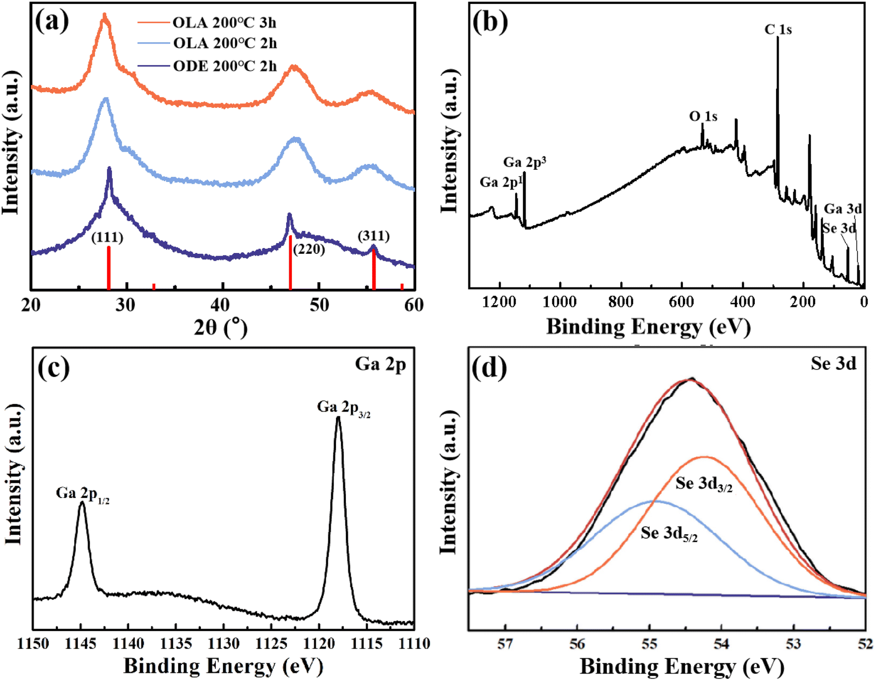
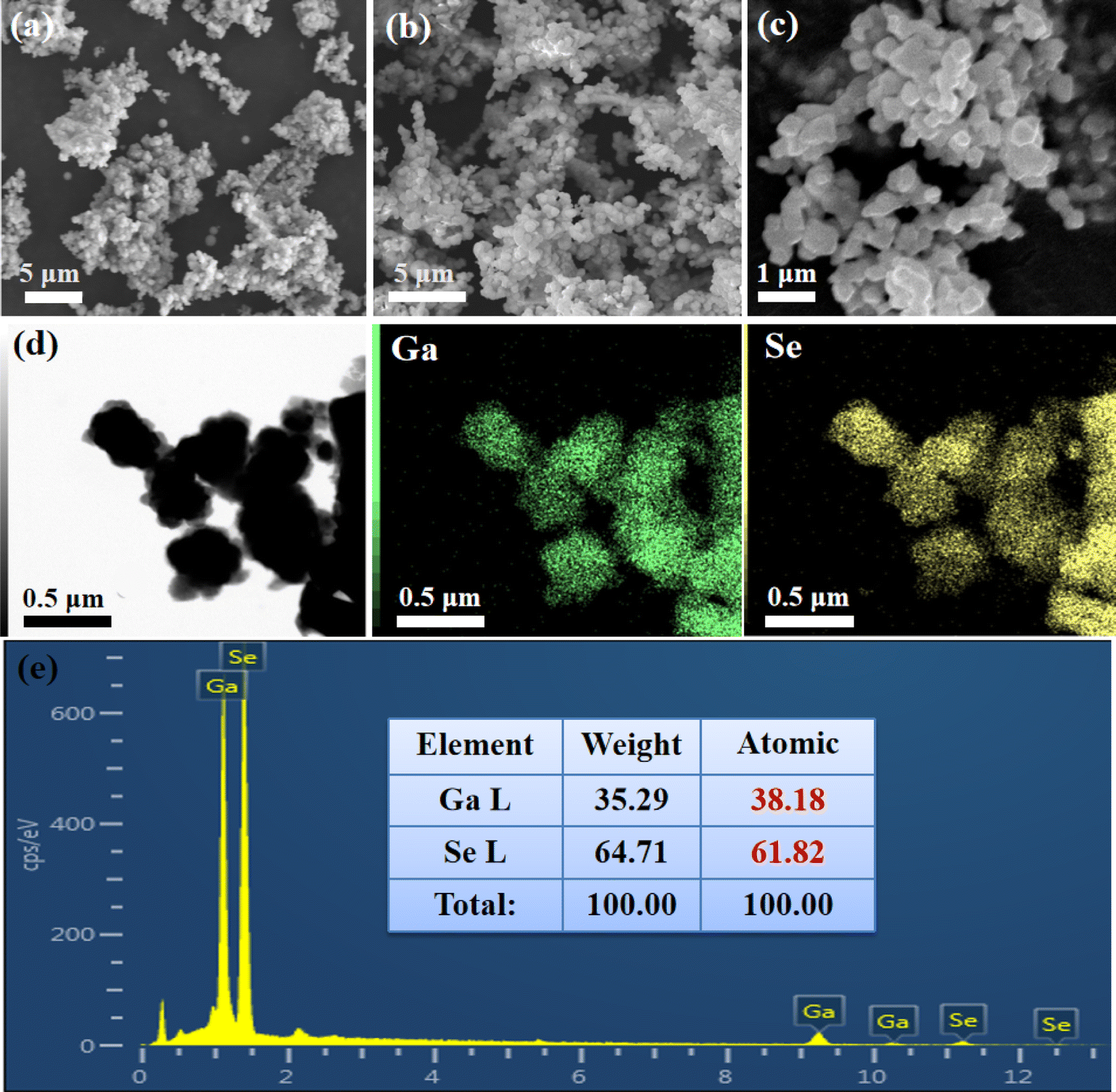
Colloidal Ga2Se3 nanoparticles were synthesized by a facile high temperature organic liquid phase method, employing gallium acetylacetonate and selenium in various solvents and at different reaction times. As depicted in Fig. 1a, all of the diffraction peaks could be indexed to the cubic Ga2Se3 (JCPDS 05-0724), revealing that the as-synthesized Ga2Se3 sample is a pure phase. XPS was utilized to further analyze the elemental compositions and chemical states of the Ga2Se3 nanoparticles. Low-resolution XPS survey confirms the presence of Ga, Se, O and C signals in Ga2Se3 sample (Fig. 1b). The observed oxygen peak can be attributed to the adsorption of air on the sample surface. In the magnified Ga-2p spectrum (Fig. 1c), two peaks located at 1144.8 eV and 1117.9 eV correspond with the Ga 2p1/2 and 2p3/2 of Ga3+.23,24 By fitting the Se-3d spectrum (Fig. 1d), the characteristic peaks at 55.1 eV and 54.2 eV correspond with the Se 3d3/2 and 3d5/2 binding energies of Se2−, agreeing well with previous reports.25 Moreover, the representative SEM images are shown in Fig. 2a–c, Ga2Se3 exhibit as highly uniform irregular nanoparticles with a diameter of about 500 nm. The TEM image and corresponding elemental mappings in Fig. 2d reveal that colocalization of the Ga and Se elements on the Ga2Se3 nanoparticles with an average atomic ratio of 38.18%![[thin space (1/6-em)]](https://www.rsc.org/images/entities/char_2009.gif) :61.82% (2:3) (Fig. 2e), in good agreement with the above XRD results.
:61.82% (2:3) (Fig. 2e), in good agreement with the above XRD results.
 | ||
| Fig. 1 (a) XRD patterns, (b–d) XPS spectra and high-resolution Ga 2p, Se 3d spectra of Ga2Se3 nanoparticles. | ||
 | ||
| Fig. 2 (a–c) SEM images, (d) corresponding TEM elemental mappings and (e) EDX spectrum of the as-prepared Ga2Se3 nanoparticles. | ||
Although Ga2Se3 pure phase has been prepared, it exhibits a wide diffraction peak (Fig. 1a). To further improve the crystallinity of Ga2Se3, the synthesized samples were annealed under vacuum conditions at temperatures of 150 °C, 200 °C, 250 °C, and 300 °C for 2 h. The XRD results (Fig. 3a) show that the main peaks of Ga2Se3 are still present and without any impurities are observed, which further confirms that the Ga2Se3 samples did not undergo phase transformation after annealing. Post-annealing promotes the diffusion of atoms within a material, leading to an orderly realignment of atomic structures. This process effectively reduces grain boundaries and defects.26 As a result, the crystallinity of Ga2Se3 samples is significantly improved after undergoing annealing. Notably, the sample annealed at 200 °C has the strongest XRD diffraction peak intensity, followed by a decrease in peak intensity with increasing annealing temperature. This suggests that the grain growth may be effectively promoted at 200 °C. Next, to further clarify the changes in XRD diffraction peaks after annealing, the thermal stability of the Ga2Se3 sample was carried out (Fig. S1†). From the thermogravimetric curve of Ga2Se3, weight loss is observed starting around about 200 °C, which is consistent with the decomposition temperature of selenium.27 Moreover, upon annealing at 300 °C, the weight of Ga2Se3 nanoparticles decreases to 80% of the initial mass. Consequently, the decrease in peak intensity beyond 200 °C can be ascribed to the formation of selenium vacancies and the concomitant reduction in Ga2Se3 mass.
 | ||
| Fig. 3 (a) XRD patterns, (b) transmission spectra, (c) (αhv)2–hv curves and (d) band gap values of Ga2Se3 sample at different annealing temperatures. (e and f) Calculated energy band structures of Ga2Se3 and expand Ga2Se3 using HSE06 functional. | ||
The optical bandgaps of Ga2Se3 samples were determined by UV-vis-NIR transmission spectra, as shown in Fig. 3b. The transmittance of Ga2Se3 nanoparticles had a sharply decline at about 570 nm and decreased almost to zero near 400 nm. And the absorption band edge of Ga2Se3 samples are continuously bule-shifted with increasing annealing temperatures. The bandgap was calculated according to the equation (αhv)n = C(hv − Eg), where C is a constant, α is the absorption coefficient, Eg is band gap, hv is the photon energy and n equals to 2 for direct inter-band transition.28 By plotting (αhv)2–hv curves (Fig. 3c) and extrapolating the linear sections of the curves to the x-axis, the band gaps were determined to be 2.50, 2.61, 2.66, 2.73, and 2.80 eV for the untreated and annealed samples at 150, 200, 250, and 300 °C, respectively (Fig. 3d). Table S1† shows the lattice constants and cell volumes calculated from the XRD patterns in Fig. 3a. It is observed that annealing at various temperatures leads to a large lattice constant (a) compared to the original Ga2Se3. The non-monotonic increase in lattice constants (a) at 250 °C may be attributed to lattice distortion effects. And the lattice distortion relative to Ga2Se3 for annealing at 150, 200, 250, and 300 °C is ΔV = 3.46, 4.85, 3.37 and 4.40 Å3. At high temperatures, atomic or phonon vibrations significantly affect the band gap through electron–phonon interactions and lattice thermal expansion, as observed in semiconductors like black phosphorus and CsSnI3.29,30 To further investigate the influence of lattice parameters and chemical bonds on the band gap of Ga2Se3, we conducted first-principles calculations. As depicted in the band structure in Fig. 3e, the untreated Ga2Se3 has a band gap of 2.38 eV, which is a direct band gap material due to the alignment of the valence band maximum and conduction band minimum at the same high-symmetry point. As the lattice constant of Ga2Se3 increases from 5.219 Å to 5.438 Å, the lattice expansion weakens the interaction between atoms, resulting in a decrease in the overlap of Ga and Se atomic orbitals (Fig. 3f). This separation of electronic states in the valence band and conduction band leads to an increase in the band gap to 2.42 eV.
Fig. 4a shows the XRD patterns of different Cr-doped Ga2Se3 nanomaterials. The main peaks (111) and (220) of Ga2Se3 shift to the higher angle with increasing Cr dopant content (0 < x ≤ 0.6), which is attributed to the replacement of Cr3+ (69 pm) by the smaller Ga2+ (62 pm). And the corresponding lattice constants and unit cell volumes of the Ga2−xCrxSe3 were summarized in Table S2.† However, when the Cr doping content reaches 0.6, the diffraction peak at 33° can correspond to the hexagonal Cr2Se3 (−112) crystal plane. These results indicate that Cr ions can be successfully doped into Ga2Se3 lattice, while the excessive Cr ions will combine with Se ions to form new phase Cr2Se3. XPS spectra (Fig. 4b) further confirm the presence of Ga, Se and Cr in the Ga2−xCrxSe3 (x = 0.4) sample. From Cr-3d spectrum in Fig. 4c, the chemical states of Cr 2p1/2 and 2p3/2 can be identified from the peaks at binding energies of 586.5 eV and 576.2 eV, which proves the sample is indeed doped with Cr element.31 And the Ga-2p and Se-3d spectra in Ga2−xCrxSe3 (x = 0.4) are the same as those in Ga2Se3 (Fig. 4d and e). The content of Cr, Ga and Se elements in Ga2−xCrxSe3 samples was analyzed using EDX spectra, as shown in Fig. S3 and Table S3.† The histogram in Fig. 4 signifies that as the doping amount (x) increases, the amount of chromium gradually increases, while the content of gallium gradually decreases. Significantly, the total cation content (Cr3+ + Ga3+) and the total anion content (Se2−) maintained a constant ratio of 2:3. This further confirms the partial substitution of Ga cations by Cr cations, indicating a substitutional doping has occurred between cations.
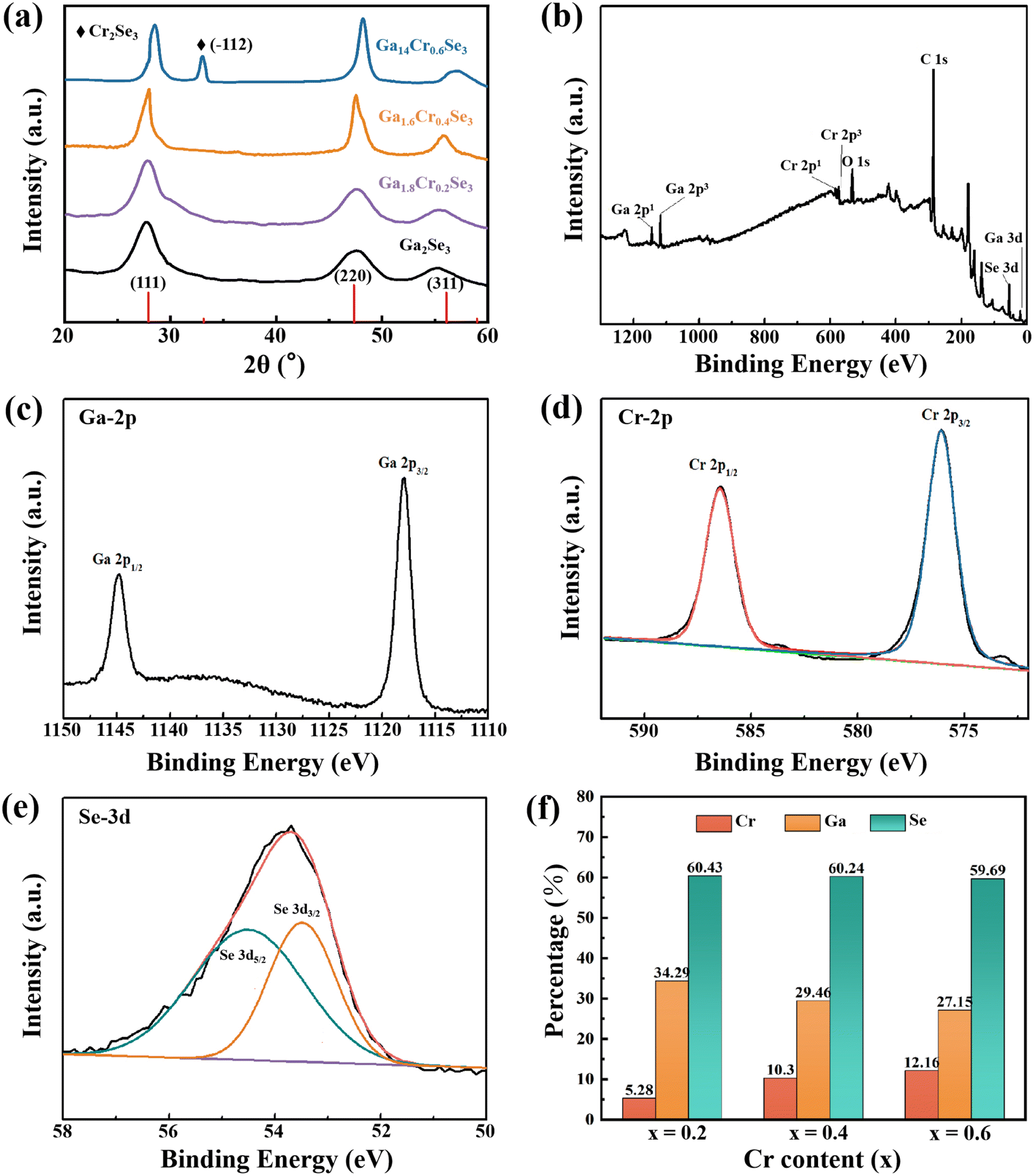 | ||
| Fig. 4 (a) XRD patterns of different Cr-doped Ga2Se3 nanomaterials. (b) XPS spectra and (c–e) high-resolution spectra of Cr 2p, Ga 2p and Se 3d in Ga1.6Cr0.4Se3 sample. (f) EDX analyses of Ga2−xCrxSe3 (0 ≤ x ≤ 0.6) with different Cr concentrations. | ||
Fig. 5 shows TEM images of Ga2−xCrxSe3 with different Cr dopants. All Ga2−xCrxSe3 samples are composed of ultra-thin nanosheets with a size of about 100 nm and are well dispersed (Fig. 5a–c). In the high-resolution TEM image of the Ga1.6Cr0.4Se3 sample (Fig. 5d), a clear lattice fringe of 0.294 nm is observed, which is smaller than the lattice spacing (0.314 nm) on the (111) plane of cubic Ga2Se3. It is consistent that the (111) peak has a slight blueshift in the XRD pattern. The elements Cr, Ga and Se are uniformly distributed in Ga1.6Cr0.4Se3 ultra-thin nanosheets (Fig. 5e). Thus, Cr doping in Ga2Se3 facilitates the formation of ultrathin nanosheets.
 | ||
| Fig. 5 (a–c) TEM images of Ga2−xCrxSe3 (0 ≤ x ≤ 0.6) nanosheets with different Cr concentrations. (d) Enlarged TEM, HRTEM and (e) corresponding elemental mappings images of Ga1.6Cr0.4Se3 nanosheets. | ||
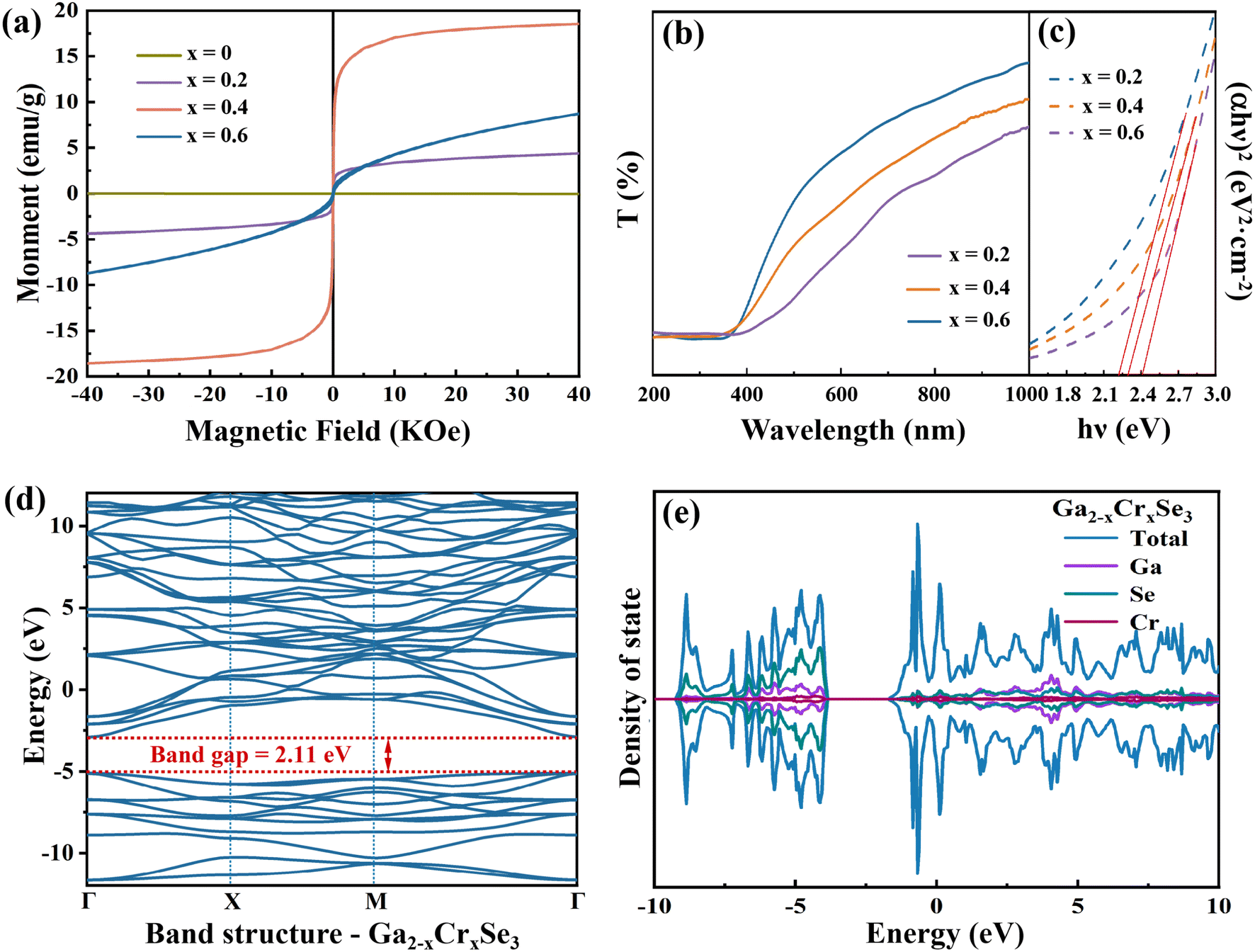
The magnetic hysteresis loops (Fig. 6a) of Ga2−xCrxSe3 (0 ≤ x ≤ 0.6) at 5 K were obtained by PPMS. When x = 0, Ga2Se3 nanoparticles show a diamagnetic signal. The M–H curve is a straight line passing through the second and fourth quadrants, and the magnetic moment is almost 0. As the incorporation of Cr ions into the Sb2Se3 lattice, the system began to exhibit ferromagnetism. When x = 0.4, the magnetization can reach up to 18.0 emu g−1 at 40 kOe. The 3d orbital partially occupied by Cr element is the main magnetic moment source. However, when the Cr content increases to x = 0.6, the system exhibits antiferromagnetism. This is consistent with the reported antiferromagnetism of Cr2Se3 nanostructures with non-collinear spin configuration, which confirms the XRD results.
 | ||
| Fig. 6 (a) M–H loops measured at 5 K, (b) transmission spectra, (c) (αhv)2–hv curves of the Ga2−xCrxSe3 (0 ≤ x ≤ 0.6) nanosheets with different Cr concentrations. (d and e) Calculated energy band structure and DOS plot of Ga2−xCrxSe3 sample. | ||
Cr doping not only induces ferromagnetism in Ga2−xCrxSe3 system, but also affects the band gaps of Ga2Se3. From the transmission curves and plotting (αhv)2–hv curves (Fig. 6b and c), it can be seen that the band gaps of Ga2−xCrxSe3 are estimated as 2.42, 2.30, and 2.23 eV when the Cr content (x) is 0.2, 0.4 and 0.6. The introduction of Cr ions significantly alters the electronic structure of Ga2Se3. The detailed analysis of the band structure and DOS calculations demonstrates that the newly introduced Cr ion density peaks appear near the Fermi level, increasing the density of states around this region. This increase reduces the energy required for electrons to transition from the valence band to the conduction band, resulting in a decrease in the band gap of Ga2−xCrxSe3 (2.11 eV). Combined with the band gaps of Ga2Se3 annealed at different temperatures (2.50–2.80 eV), the band gaps of the Ga2−xCrxSe3 nanomaterials can achieve continuous changes in the range of 2.23 eV to 2.80 eV.
The photoelectrochemical performances of Ga2Se3 and Ga2−xCrxSe3 (x = 0.4) were investigated through the hydrogen evolution reaction (HER) in 0.5 mol per L H2SO4 aqueous solution. The LSV curves of both Ga2Se3 and Ga1.6Cr0.4Se3 (Fig. S4†) show positive response to simulated light (a 300 W Xe lamp) in the range of 0 to −0.6 V. Notably, the doped Ga1.6Cr0.4Se3 always displays superior onset potentials for HER compared to pure Ga2Se3 in both light and dark conditions. I–t curves in Fig. 7a and b further indicate the Ga2Se3 and Ga1.6Cr0.4Se3 have good photocurrent response in the whole 600 s switching visible light on/off cycle. And the photocurrent densities could be effectively modulated by varying the bias voltage. Specifically, the photocurrent density of Ga1.6Cr0.4Se3 increased from 0.2 to 15.5 mA cm−2, with the applied bias potentials increasing from −0.2 to −0.6 V, respectively. This enhancement is attributed to the role of bias potentials in facilitating the separation and migration rate of photogenerated electron–hole pairs. Additionally, the lower impedance and charge transfer resistance of Ga1.6Cr0.4Se3, confirmed by EIS measurements (Fig. 7c and d), suggest that a certain amount of Cr doping significantly improves photoelectrocatalytic hydrogen evolution performance. Additional N2 adsorption/desorption isotherms (Fig. 8a and b) display typical type IV behavior according to the IUPAC classification, and pore size distribution curves (Fig. 8c and d) confirm that both materials are primarily mesoporous. Notably, the BET surface area of Ga1.6Cr0.4Se3 was measured at 39.1 m2 g−1, significantly higher than the 7.9 m2 g−1 recorded for Ga2Se3 (Table S4†). The large surface area should favor the rapid transfer of electrons during photoelectrocatalytic processes, which is consistent with the catalytic results.
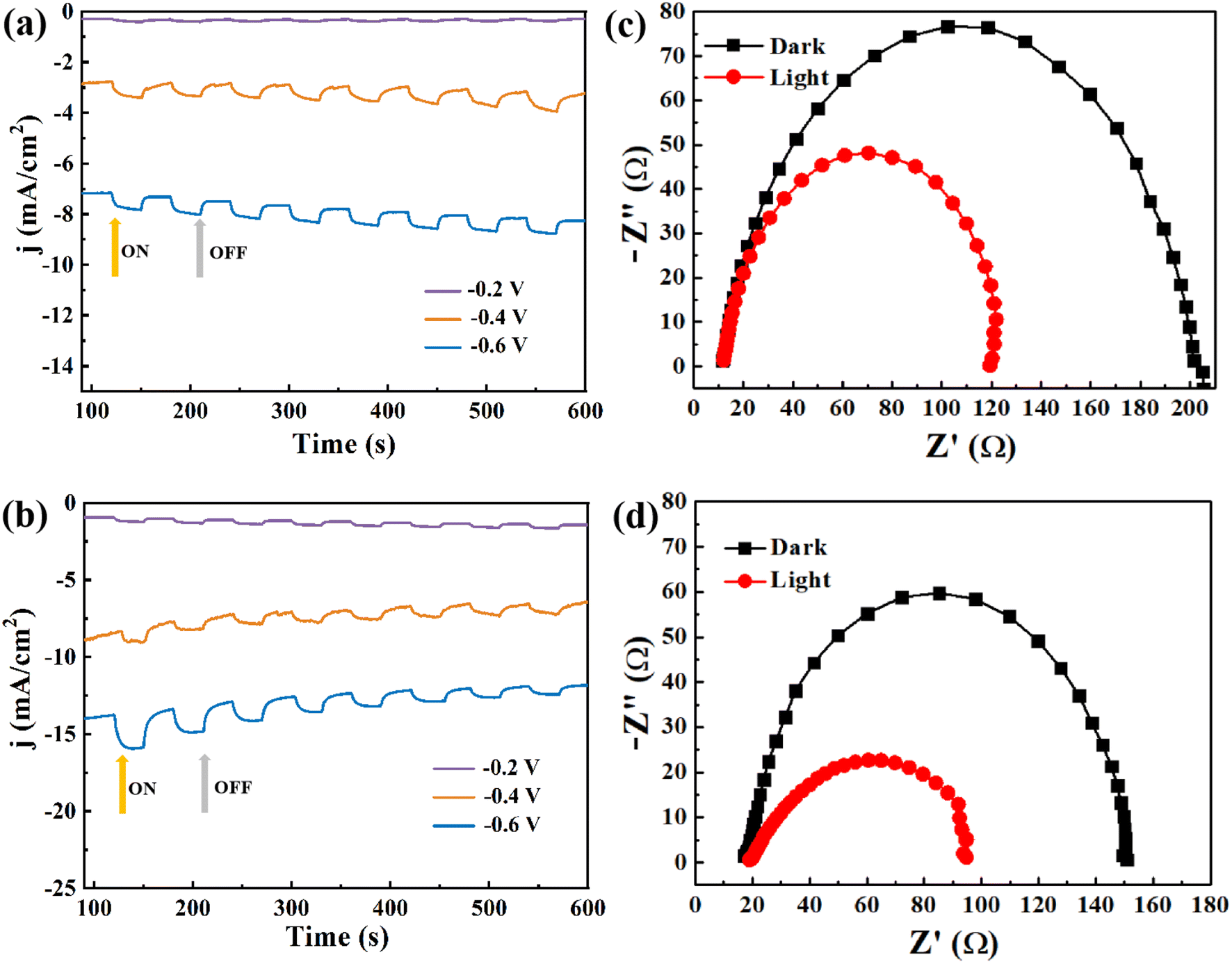 | ||
| Fig. 7 (a and b) I–t curves and (c and d) EIS curves of Ga2Se3 nanoparticles and Ga1.6Cr0.4Se3 nanosheets. | ||
 | ||
| Fig. 8 (a and b) N2 adsorption/desorption isotherms and (c and d) the corresponding pore-size distribution curves of Ga2Se3 nanoparticles and Ga1.6Cr0.4Se3 nanosheets. | ||
4. Conclusion
In summary, we have successfully synthesized Ga2Se3 nanoparticles and Ga2−xCrxSe3 nanosheets using high temperature organic liquid phase method. The optical band gaps of Ga2−xCrxSe3 can be continuously adjusted in the range of 2.23 to 2.80 eV with changing the annealing temperature (150–300 °C) and introduction of different Cr doping concentrations. The magnetic study results indicate that moderate Cr doping (x < 0.4) induces a transition in Ga2Se3 from paramagnetic to ferromagnetic behavior, with a magnetization intensity reaching 18.0 emu g−1 at 40 kOe. Besides, photoelectrochemical studies reveal that Ga1.6Cr0.4Se3 nanosheets exhibit superior hydrogen evolution performance compared to Ga2Se3 nanoparticles. Therefore, the dual modulation of bandgap and magnetic properties through Cr doping presents a promising avenue for the development of high-performance opto-electromagnetic devices.Data availability
The data that support the findings of this study are available from the corresponding author upon reasonable request.Conflicts of interest
There is no conflict to declare.Acknowledgements
This work was supported by the National Natural Science Foundation of China (52301244, 52371191, 52202340) and the Youth Science Foundation of Shanxi Province (202203021222218).References
- H. Kim, D. Monllor-Satoca, W. Kim and W. Choi, Energy Environ. Sci., 2015, 8, 247–257 RSC.
- Q. Deng, X. Li, H. Si, J. Hong, S. Wang, Q. Feng, C. X. Hu, S. Wang, H. L. Zhang, K. Suenaga and H. Xu, Adv. Funct. Mater., 2020, 30, 2003264 CrossRef CAS.
- Z. Dai, L. Liu and Z. Zhang, Adv. Mater., 2019, 31, 1805417 CrossRef CAS PubMed.
- Q. Lv and R. Lv, Carbon, 2019, 145, 240–250 CrossRef CAS.
- M. Kapilashrami, Y. Zhang, Y. S. Liu, A. Hagfeldt and J. Guo, Chem. Rev., 2014, 114, 9662–9707 CrossRef CAS PubMed.
- J. H. Clark, M. S. Dyer and R. G. Palgrave, J. Am. Chem. Soc., 2011, 133, 1016–1032 CrossRef CAS PubMed.
- S. Dai, X. Yan, C. R. Ward, J. C. Hower, L. Zhao, X. Wang, L. Zhao, D. Ren, and R. B. Finkelman, Coal Geology of China, Area Studies, London, 2020 Search PubMed.
- Z. Lu, G. P. Neupane, G. Jia, H. Zhao, D. Qi, Y. Du, Y. Lu and Z. Yin, Adv. Funct. Mater., 2020, 30, 2001127 CrossRef CAS.
- K. Xu, L. Yin, Y. Huang, T. A. Shifa, J. Chu, F. Wang, R. Cheng, Z. Wang and J. He, Nanoscale, 2016, 8, 16802–16818 RSC.
- X. Li, L. Li and M. Wu, Mater. Today Phys., 2020, 15, 100229 CrossRef.
- N. Balakrishnan, Z. R. Kudrynskyi, M. W. Fay, G. W. Mudd, S. A. Svatek, O. Makarovsky, Z. D. Kovalyuk, L. Eaves, P. H. Beton and A. Patanè, Adv. Opt. Mater., 2014, 2, 1064–1069 CrossRef CAS.
- H. Cai, Y. Gu, Y. C. Lin, Y. Yu, D. B. Geohegan and K. Xiao, Appl. Phys. Rev., 2019, 6, 041312 Search PubMed.
- C. H. Ho, X. R. Lai, C. A. Chuang, W. L. Kuo and K. K. Tiong, Adv. Photonics Res., 2021, 2, 2000110 CrossRef CAS.
- W. Xue, Q. Jiang, F. Wang, R. He, R. Pang, H. Yang, P. Wang, R. Yang, Z. Zhong, T. Zhai and X. Xu, Small, 2022, 18, 2105599 CrossRef CAS PubMed.
- G. Y. Huang, N. M. Abdul-Jabbar and B. D. Wirth, J. Phys.: Condens.Matter, 2013, 25, 225503 CrossRef PubMed.
- M. Isik and N. M. Gasanly, Vacuum, 2020, 179, 109501 CrossRef CAS.
- C. H. Ho, ACS Omega, 2020, 5, 18527–18534 CrossRef CAS PubMed.
- C. A. Chuang, M. H. Lin, B. X. Yeh and C. H. Ho, RSC Adv., 2018, 8, 2733–2739 RSC.
- A. Ravagli, C. Craig, G. A. Alzaidy, P. Bastock and D. W. Hewak, Adv. Mater., 2017, 29, 1606329 CrossRef PubMed.
- G. Y. Huang, N. M. Abdul-Jabbar and B. D. Wirth, Acta Mater., 2014, 71, 349–369 CrossRef CAS.
- K. George, C. H. de Groot, C. Gurnani, A. L. Hector, R. Huang, M. Jura, W. Levason and G. Reid, Chem. Mater., 2013, 25, 1829–1836 CrossRef CAS.
- C. S. Jung, F. Shojaei, K. Park, J. Y. Oh, H. S. Im, D. M. Jang, J. Park and H. S. Kang, ACS Nano, 2015, 9, 9585–9593 CrossRef CAS PubMed.
- T. Zhang, Y. Li, Y. Zhang, Q. Feng, J. Ning, C. Zhang, J. Zhang and Y. Hao, J. Alloys Compd., 2021, 859, 157810 CrossRef CAS.
- C. V. Ramana, D. Das, G. Gutierrez, F. S. Manciu and V. Shutthanandan, J. Mater. Sci., 2022, 57, 11170–11188 CrossRef CAS.
- H. Yang, Y. Wu, L. Y. Hu, J. J. Wang, F. Wang and X. H. Xu, Rare Met., 2023, 42, 189–197 CrossRef CAS.
- C. Kim, K. Kurosaki, M. Ishimaru, H. Muta and S. Yamanaka, J. Electron. Mater., 2011, 40, 999–1004 CrossRef CAS.
- D. Sun, S. Xu, L. Zhang, Z. Chen, Y. Ge, N. Wang, X. Liang, C. Wei, Y. Zhao and X. Zhang, J. Semicond., 2015, 36, 044009 CrossRef.
- J. I. Pankove, Optical Processes in Semiconductors, Courier Corporation, 1975 Search PubMed.
- C. E. P. Villegas, A. R. Rocha and A. Marini, Nano Lett., 2016, 16, 5095–5101 CrossRef CAS PubMed.
- C. Yu, Z. Chen, J. J. Wang, W. Pfenninger, N. Vockic, J. T. Kenney and K. Shum, J. Appl. Phys., 2011, 110, 063526 CrossRef.
- H. Yang, F. Wang, H. Zhang, L. Guo, L. Hu, L. Wang, D. J. Xue and X. Xu, J. Am. Chem. Soc., 2020, 142, 4438–4444 CrossRef CAS PubMed.
Footnote |
| † Electronic supplementary information (ESI) available. See DOI: https://doi.org/10.1039/d4ra03028a |
| This journal is © The Royal Society of Chemistry 2024 |