
 Open Access Article
 This Open Access Article is licensed under a Creative Commons Attribution-Non Commercial 3.0 Unported Licence
Ion migration and dark current suppression in quasi-2D perovskite-based X-ray detectors†
Zhenting Yanga,
Aimiao Qinb,
Haiqing Qinc,
Zhenlin Lid,
Yong Xiang ae,
Hao Liuf,
Jinyu Qiug and
Xinyu Wang*a
ae,
Hao Liuf,
Jinyu Qiug and
Xinyu Wang*a
aSchool of Materials and Energy, University of Electronic Science and Technology of China, Chengdu, China. E-mail: xinyuwang@uestc.edu.cn
bKey Laboratory of New Processing Technology for Nonferrous Metal & Materials, Ministry of Education/Guangxi Key Laboratory of Optical and Electronic Materials and Devices, Guilin University of Technology, Guilin, China
cGuangxi Key Laboratory of Superhard Material, National Engineering Research Center for Special Mineral Material, Guangxi Technology Innovation Center for Special Mineral Material, China Nonferrous Metal (Guilin) Geology And Mining Co., Ltd, Guilin, China
dDepartment of Radiology, West China Hospital, Sichuan University, Chengdu, China
eTianfu Jiangxi Laboratory, Chengdu, China
fBOE Technology Group Co., Ltd, Beijing, China
gChengdu Experimental Foreign Languages School International Department, Chengdu, Sichuan, China
First published on 14th June 2024
Abstract
Cesium-based lead-free double perovskite materials (Cs2AgBiBr6) have garnered significant attention in the X-ray detection field due to their environment friendly characteristics. However, their substantial ion migration properties lead to large dark currents and detection limits in Cs2AgBiBr6-based X-ray detectors, restricting the detection performance of the device. In terms of process technology, ultrasonic spraying is more suitable than a spin-coating method for fabricating large-area, micron-scale perovskite thick films, with higher cost-effectiveness, which is crucial for X-ray detection. This work introduces a BA+ (BA+ = CH3CH2CH2CH2NH3+, n-butyl) source into the precursor solution and employs ultrasonic spraying to fabricate quasi-two-dimensional structured polycrystalline (BA)2Cs9Ag5Bi5Br31 perovskite thick films, developing a low-cost, eco-friendly X-ray detector with low dark current density and low detection limit. Characterization results reveal that the ion migration activation energy of (BA)2Cs9Ag5Bi5Br31 reaches 419 meV, approximately 17% higher than that of traditional three-dimensional perovskites, effectively suppressing perovskite ion migration and subsequently reducing the dark current. The (BA)2Cs9Ag5Bi5Br31-based X-ray detectors exhibit high resistivity (about 1.75 × 10¹⁰ Ω cm), low dark current density (66 nA cm−2), minimal dark current drift (0.016 pA cm−1 s−1 V−1), and detection limit (138 nGyair s−1), holding considerable promise for applications in low-noise, low-dose X-ray detection.
1. Introduction
As the era progresses, with the development of technology and the increasing needs of people, high-energy ionizing radiation X-ray detection technology plays a crucial role in fields such as medical imaging, security imaging, and industrial non-destructive testing.1–3 Among current X-ray direct detection technologies, commercial detectors employing amorphous selenium (α-Se) as the photoabsorbing layer have been developed.4 However, due to their lower carrier mobility-lifetime product, lower atomic number, and the need for a higher operating electric field for effective operation, they exhibit lower sensitivity and higher detection limits in practical applications.5 Other traditional semiconductor materials, such as cadmium telluride (CdTe) and cadmium zinc telluride (CdZnTe), offer higher absorption rates for high-energy X-Rays compared to amorphous selenium, but these materials require high-temperature melting methods for preparation, making them relatively expensive.6 The development of new materials is urgently needed to meet high-performance detection requirements while also considering cost and fabrication process optimizations.Halide perovskite materials, since their introduction, have not only demonstrated excellent photoelectric conversion efficiency in the photovoltaic field but also meet the requirements for high-performance X-ray detection due to their high X-ray absorption coefficient, high carrier mobility-lifetime product μτ, large resistivity, and low cost.7–9 Among the halide perovskites reported, lead-based halides containing high atomic number Pb elements, have stronger X-ray absorption capabilities, resulting in high sensitivity devices, and have long been a hot research material in the field.10,11 However, the toxic nature of lead poses certain barriers to their commercial development.
Lead-free double perovskite Cs2AgBiBr6 single crystals have shown excellent X-ray response performance while meeting green and environment friendly requirements. Tang Jiang's team12 pioneered the development of X-ray direct detectors based on Cs2AgBiBr6 single crystals grown via a low-cost solution, achieving a detector sensitivity of 105 μC Gyair−1 cm−2 and a minimum detection limit of 59.7 nGyair s−1, with good thermal and radiation stability. This discovery provides an important material basis for the development of efficient and environment friendly X-ray detectors. In fact, the preparation process of single crystals is relatively complex and has low compatibility with the transistor (TFT) backplane used in the imaging end. Compared to single crystals, polycrystalline thick films are more suitable for low-cost and large-area X-ray detection applications.13 Despite significant progress in perovskite-based X-ray detectors, challenges remain due to the intrinsic ion migration within perovskite compounds. Charged ions within the material can be driven by external electric fields, leading to ion migration along defects and other channels, which can generate significant noise and baseline drift issues, adverse for achieving lower detection limits and high stability devices.14 Especially in polycrystalline materials, the vast number of grain boundaries makes ions more inclined to migrate along defects at the boundaries, further exacerbating noise and baseline drift issues. Therefore, further suppression of ion migration in polycrystalline perovskites is key to achieving high stability X-ray detectors.
Studies have found that for perovskite polycrystalline films, various methods such as producing a thick film with a compact structure15,16 to reduce voids, growing large-size grains,17 passivating grain boundaries,18 and dimension control,19 can reduce ion migration in perovskite materials. Among these, a widely studied method in dimension control strategies involves adding large organic cations (such as phenethylammonium, PEA+,20 butylammonium, BA+,21 etc.) to the perovskite precursor solution. This separates part of the [BX6]4− octahedra originally connected in a vertex-sharing manner in the three-dimensional perovskite structure, relying on van der Waals forces between organic cations to stably combine, thereby inducing a layered RP structure  (where A′ is a substituted large-size organic cation, A is an inorganic cation group, B is a high atomic number metal cation like Pb2+ or Sn2+, and X is one or a combination of halogen ions such as I−, Br−, Cl−, with n representing the number of inorganic octahedral layers, i.e., the inorganic layer number in low-dimensional perovskites). In 2022, Yukta and others22 successfully prepared X-ray detectors based on pure two-dimensional RP structure (BA)2PbI4 single crystals, featuring high resistivity of 2.60 × 10¹¹ Ω cm and a low detection limit of 241 nGyair s−1, demonstrating excellent radiation and environmental stability. In the same year, Zhang and others23 adjusted the dimension of RP perovskite materials by the reaction between methylamine gas and the RP perovskite precursor, achieving a high degree of control over ion migration characteristics in perovskites through BA2MAn−1PbnI3n+1·xCH3NH2 series perovskites. This low-dimensional structure design of interlaced organic and inorganic layers effectively blocks ion migration pathways at the microscopic level, significantly suppressing ion migration capability.
Xu and others21 obtained (BA)2CsAgBiBr7 with a quasi two-dimensional structure from a saturated solution using temperature cooling technology, and generated a sensitivity of 4.2 μC Gyair−1 cm−2 under an X-ray source, laying the foundation for the application of low dimensional double perovskite Cs2AgBiBr6 materials in the field of X-ray detection. Zhang and others24 prepared a quasi two-dimensional structure of (BA)2CsAgBiBr7 by introducing organic cation BA+, and grown centimeter level lead-free perovskite heterocrystals: (BA)2CsAgBiBr7/Cs2AgBiBr6 through in situ epitaxy technology, exhibiting a high sensitivity of 206 μC Gyair−1 cm−2. Although these studies demonstrate the enormous potential of quasi two-dimensional perovskites in the field of X-ray detection, they further demonstrate the enormous potential of quasi two-dimensional perovskite materials in the field of X-ray detection. However, most of the studies on low dimensional materials of Cs2AgBiBr6 mainly focused on single crystal materials, which are difficult to meet the needs of X-ray detection applications for large-area growth due to their small size. In fact, polycrystalline thick films are more suitable for low-cost, large-area X-ray detection scenarios than single crystal materials. Nonetheless, research reports on dimension control of polycrystalline Cs2AgBiBr6 materials remain relatively scarce. Therefore, we have made improvements to address the shortcomings of existing research and systematically explored the potential of quasi two-dimensional double perovskite polycrystalline materials in X-ray detection applications.
This study adds the large organic molecule butylammonium cation BA+ to the three-dimensional perovskite Cs2AgBiBr6 precursor solution, constructing a quasi-two-dimensional perovskite structure, and uses ultrasonic spraying (Note 1, ESI†) to prepare polycrystalline thick films with different inorganic layer numbers n on conductive substrates. Through systematic characterization of the film's morphology, orientation, and element distribution, the study investigates the control mechanism of butylammonium bromide BABr introduction on the crystal dimension of Cs2AgBiBr6 perovskite polycrystalline thick films. The study shows that25 the introduction of BA+ from BABr leads to the transformation of Cs2AgBiBr6 into an  RP-type quasi-two-dimensional structure, where n represents the number of inorganic layers between the organic spacing cations BA+. This work synthesized n = ∞ (which is pure Cs2AgBiBr6), n = 10 (which is (BA)2Cs9Ag5Bi5Br31), and n = 6 (which is (BA)2Cs5Ag3Bi3Br19) dual perovskite systems, with the material's quasi-two-dimensional inorganic layer number inversely related to n, i.e., the smaller the n value, the more inorganic layers in the Cs2AgBiBr6 perovskite system. The article systematically studies the relationship between different inorganic layer numbers and their ion migration characteristics, selecting the quasi-two-dimensional cesium-based double perovskite system (BA)2Cs9Ag5Bi5Br31 with the highest activation energy. Based on this material system, an X-ray detector was fabricated, successfully suppressing dark current and lowering the detection limit.
2. Method
2.1 Materials
Cesium bromide (CsBr, 99.999%) was purchased from Xi'an Bathsun Energy Technology Co., Ltd, silver bromide (AgBr, 98%), bismuth bromide (BiBr3, ≥98%), butylammonium bromide (n-BABr, >98.0%), dimethyl sulfoxide (DMSO, >99.8% (GC)), N,N-dimethylformamide (DMF, anhydrous grade), and polyvinylpyrrolidone (PVP, K60) were obtained from Aladdin Reagent Co., Ltd. All materials were used as received without further purification.2.2 Material synthesis
0.6 g of PVP was dissolved in 5 ml of DMF and stirred at 50 °C in a water bath for 5 hours to obtain a PVP solution. Then, a PVP thin film was formed on the substrate via spin-coating as an intermediate layer and was cross-linked and kept warm in a vacuum oven for 0.5 hours. The spin-coating parameters were set as follows: first spin-coated at 700 rpm for 7 seconds, then at 3000 rpm for 3 seconds.For the preparation of quasi-two-dimensional perovskites with different inorganic layer numbers, according to the general chemical formula  the stoichiometric ratio of components was adjusted.26 CsBr, AgBr, BiBr3, and n-BABr powders were mixed in the required molar ratio to prepare precursor solutions for cesium-based lead-free perovskites with n = 6 (i.e., (BA)2Cs5Ag3Bi3Br19) and n = 10 (i.e., (BA)2Cs9Ag5Bi5Br31). Here, A′ represents the organic cation BA+ substituting the inorganic A-site cation Cs+, and B denotes Ag or Bi.
Taking n = 10, i.e., (BA)2Cs9Ag5Bi5Br31 quasi-two-dimensional perovskite as an example, 3.06 g CsBr, 1.50 g AgBr, 3.59 g BiBr3, and 0.49 g n-BABr were weighed and added into a clean glass bottle, dissolved in 40 ml DMSO, and the bottle was sealed and stirred overnight on a magnetic stirrer. After the perovskite solution became homogeneous without floating particles, 40 ml of DMF was added, and the mixture was stirred for 3 hours to obtain a clear, transparent perovskite precursor solution.
Secondly, a three-dimensional structure Cs2AgBiBr6 perovskite, i.e., n = ∞, was prepared as the control group for this study. 3.40 g CsBr, 1.50 g AgBr, 3.59 g BiBr3 powders were dissolved in 40 ml DMSO, and after overnight stirring, 40 ml DMF was added to dilute the original solution.
Different inorganic layer numbers (n = ∞, 10, and 6) of perovskite light-absorbing layers were prepared using ultrasonic spray coating, with a working power set to 2.5 W to atomize the precursor solution, assisted by nitrogen gas, and the substrate temperature was set to 140 °C. After deposition, the samples were cooled to room temperature at a rate of 1 °C min−1.
2.3 Device fabrication
Metal upper electrodes were fabricated using a silver paste scraping method to construct ITO/PVP/Perovskite/Ag devices for subsequent characterization and testing, where PVK denotes the perovskite light-absorbing layer. A mask with an electrode area of 0.02 cm2 was selected as the scraping tool. Before scraping, the mask was ultrasonically cleaned in anhydrous ethanol for 15 minutes and dried with a nitrogen gun. The mask was fixed above the sample with tape, and an appropriate amount of silver paste was applied through the electrode area of the mask and evenly scraped on the sample surface. After scraping, the device was immediately placed in an oven to dry at 60 °C for 3 hours.2.4 Characterization
Phase analysis of the samples was conducted using a Rigaku SmartLab SE X-ray diffraction (XRD) instrument with Cu target Kα radiation. A MERLIN Compact field emission scanning electron microscope (SEM) from ZEISS, Germany, was used, and energy-dispersive spectroscopy (EDS) tests were performed on the same equipment to analyze the micro-surface morphology, cross-sectional information, and element distribution. A Keithley electrometer, model 6517B, was used to measure the device's dark current and ionic conductivity, studying the material's ion migration characteristics. The response and detection limit of the detector to X-Rays were obtained by irradiating the sample with X-Rays from an X-ray tube, reading, and collecting signal data through a probe station and Keithley electrometer.3. Results and discussion
We synthesized a series of perovskite film with thicknesses in the micron range for n = ∞, 10, and 6, where n represents the number of inorganic octahedral layers. For perovskite thick films with low n-value (e.g., n = 1 and n = 2), more organic components hinder solvent evaporation and leads to excessive interfaces and defects during the formation (Fig. S1, ESI†). Additionally, these materials demonstrated high dark current densities (Fig. S4(a) and (b), ESI†). For perovskite thick films with higher n-value, n = 14 was found that its resistivity was similar to that of traditional three-dimensional perovskite (Fig. S4(c), ESI†). This indicates that materials with higher n-values are similar to three-dimensional perovskites, losing the specific advantages of quasi two-dimensional structures.3.1 Phase analysis
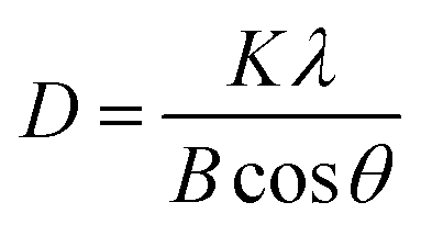
X-Ray diffraction (XRD) can be used to determine the orientation and crystallinity of perovskite thick films. Fig. 1 presents the XRD patterns and a magnified view for samples with different inorganic layer numbers n. As can be seen from Fig. 1(a), under the intercalation effect of the n-BABr organic molecule, the perovskite thick films of n = ∞, n = 10, and n = 6 show no extra impurity peaks, indicating high phase purity of the materials, which is beneficial for the transport of carriers within the materials. In the low-angle (2θ < 10°) diffraction peak range for n = 10 and n = 6, a distinct diffraction peak emerges, as the large organic cations first induce the crystal to crystallize along the (002) plane,24 the presence of the low diffraction angle peak confirms the formation of low-dimensional perovskites, consistent with XRD results of quasi-two-dimensional perovskite materials reported in other studies.23 Fig. 1(b) is a magnified view of the (002) plane diffraction angle around 6.50° from Fig. 1(a), where the full width at half maximum (FWHM) at this diffraction peak for different n values can be clearly observed. The FWHMs for n = 10 and n = 6 thick films are 0.141° and 0.154°, respectively, reflecting changes in the average grain size of the materials. According to the Scherrer formula:27
 | (1) |
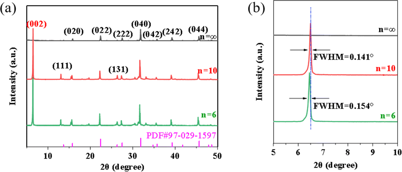 | ||
| Fig. 1 (a) XRD spectra of different n-values of perovskite; (b) XRD spectra of enlarged (200) plane. | ||
3.2 Morphological characterization
To visually demonstrate the impact of the inorganic layer number n on the surface morphology of perovskite thick films, scanning electron microscopy (SEM) was employed to characterize the surface and cross-sectional morphologies of the films. From Fig. 2(a) and (d), which respectively show the SEM surface and cross-sectional images for the n = ∞ sample, it is observed that the grain size of the n = ∞ thick film is uneven, with both large and small grains randomly distributed on the surface, leading to significant surface non-uniformity. The introduction of BA molecules can improve the wettability between the precursor solution of perovskite and the substrate (Fig. S2, ESI†), thereby achieving rapid spontaneous diffusion and surface infiltration of the solution on the substrate surface. This allows the solution to form a uniform liquid film on the substrate surface, avoiding the occurrence of liquid film shrinkage during solvent evaporation. Thanks to the wettability between the organic components and the substrate, the surfaces of n = 10 (see Fig. 2(b) and (e)) and n = 6 (see Fig. 2(c) and (f)) thick films become more uniform, exhibiting a layered structure similar to two-dimensional crystals, which visually verifies the existence of quasi-two-dimensional perovskites. Microscopic observations revealed that the n = 10 sample surface and interface possess a layered crystal structure, indicating that the introduction of BA+ successfully synthesized the quasi-two-dimensional perovskite structure. The quantity of layered crystal structures in the n = 6 sample is less than that in the n = 10 sample, a phenomenon possibly due to organic polymers coating the grain surfaces. Despite some morphological differences between the n = 10 and n = 6 thick films, their grain sizes are both relatively small (Fig. 2 and S3, ESI†). This phenomenon can be attributed to the steric hindrance effect:28–30 the organic cations not only regulate the dimensional structure but also significantly impact the crystallization kinetics of the film. Xiao and others31 also noted that increasing the proportion of BA+ in the precursor solution provides numerous nucleation sites, significantly constraining the growth of perovskite particles. These findings are consistent with our observations.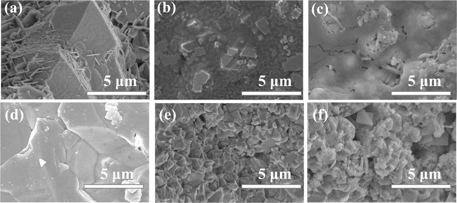 | ||
| Fig. 2 (a–c) Top-view SEM images of perovskite about n = ∞, n = 10, and n = 6, respectively; (d–f) cross-sectional SEM images of perovskite about n = ∞, n = 10, and n = 6, respectively. | ||
3.3 Elemental distribution analysis
To further determine the changes and distribution of elements in the perovskite after dimension regulation using n-BABr, energy dispersive spectroscopy (EDS) tests were conducted on perovskite thick films of the three compositions. Elements such as Cs, Ag, Bi, and Br are evenly distributed in the selected regions of the sample, without significant agglomeration, as can be seen from Fig. 3.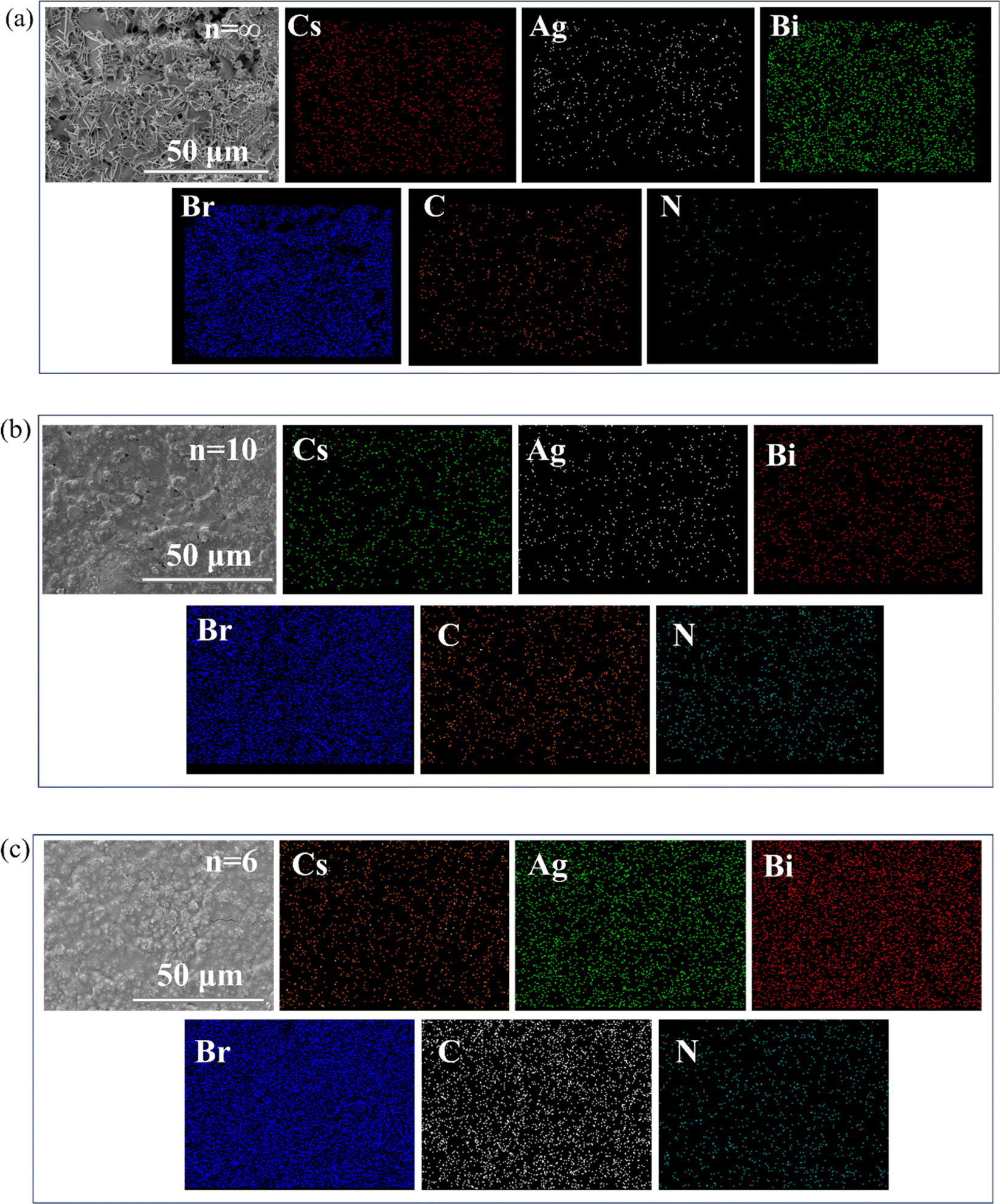 | ||
| Fig. 3 EDS mapping of perovskite about (a) n = ∞, (b) n = 10 and (c) n = 6. | ||
From the elemental atomic content bar graph shown in Fig. 4, it is clearly demonstrated that with the decrease in n value, the contents of C and N elements in the perovskite thick films gradually increase, while the content of Cs decreases. Based on the XRD and SEM analyses above, it can be inferred that the organic cation BA+ has partially replaced the inorganic cation Cs+, significantly affecting the overall structure of the material.
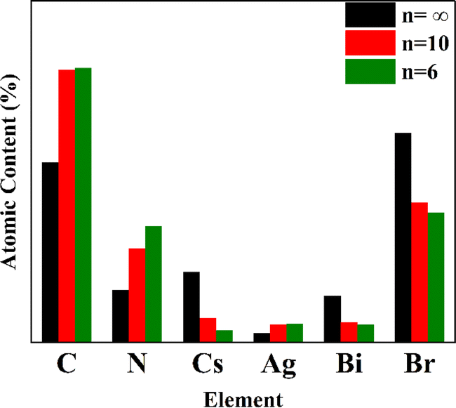 | ||
| Fig. 4 Histogram of element contents of perovskite thick films about different n values. | ||
3.4 Resistivity
To study the suppression effect of the quasi-two-dimensional structure on ion migration, resistivity tests were first conducted on perovskites with different n values. As shown in Fig. 5, the current–voltage (I–V) characteristics curves obtained under dark test conditions for each material were fitted to slopes, and the resistivity was calculated according to the formula for resistivity. The test results show that after introducing a reasonable BA organic interlayer, the resistivity of the perovskite structure with an inorganic layer number of 10, i.e., the n = 10 component, was enhanced to 1.75 × 10¹⁰ Ω cm. The increase in resistivity is attributed to the dimensional regulation of the three-dimensional perovskite structure by the large organic molecules, effectively suppressing ion migration, reducing ionic conductivity, and lowering dark current. For the n = 6 material, its resistivity was similar to that of the three-dimensional structure n = ∞, showing no significant improvement. Notably, the resistivity of the n = 6 quasi-2D perovskite formed after introducing more BA+ remains almost unchanged compared to the three-dimensional perovskite. This is primarily because the significant increase in the number of grain boundaries raises the defect density, creating channels for ion migration. This indicates that the negative impact of an increased number of grain boundaries due to the high proportion of BA+ partially offsets its ability to inhibit ion migration.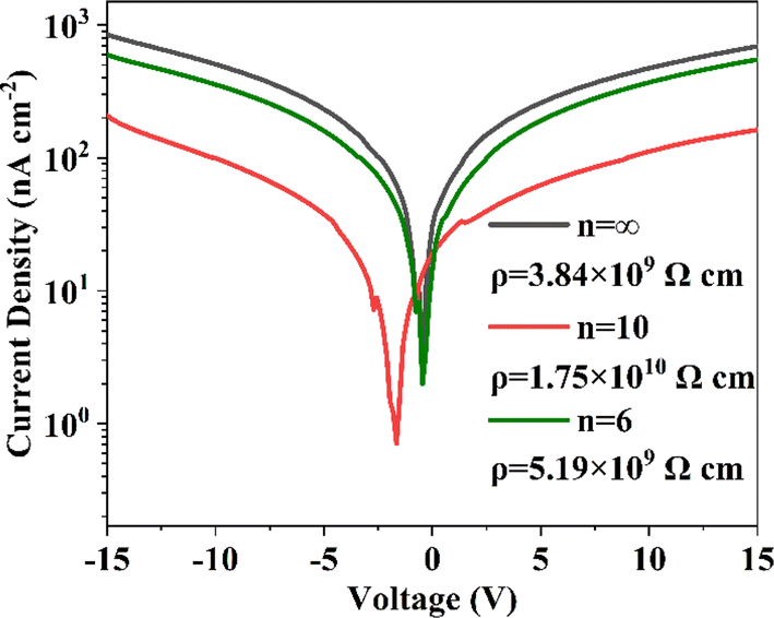 | ||
| Fig. 5 Current–voltage (I–V) curves of perovskite thick films with different n values. | ||
3.5 Ion migration characterization
To investigate the characteristics of dark current drift, the current–time (I–t) curves of all devices were tested under a single X-ray irradiation for 30 seconds at a bias electric field of 160 V mm−1. As shown in Fig. 6, among all materials, the n = 10 material exhibits the lowest dark current density, approximately 66 nA cm−2. Defining the current drift value32 as the difference in current density at the start and end points per unit time and per unit field strength, the degree and magnitude of current drift for different materials are quantified. The dark current drift values for n = 6 and n = 10 materials are less than those of the unmodified material devices, especially the n = 10 material, which exhibits higher stability in terms of dark current, with relatively small dark current drift, only 0.016 pA cm−1 s−1 V−1. This is comparable to other works involving quasi-two-dimensional materials, such as PEA2MA8Pb9I28 (Table S1, ESI†). These results indicate that the quasi-two-dimensional structure shows a clear improvement in controlling dark current drift, i.e., ion migration. Similarly to the dark current drift results, the n = 10 material also exhibits relatively small current drift under X-ray irradiation, further validating the effectiveness of the quasi-two-dimensional structure in suppressing current drift. This particularly emphasizes its general applicability under different operating conditions.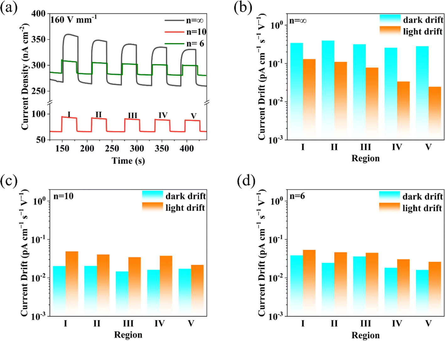 | ||
| Fig. 6 Effect of dimensional regulation on the current drift of perovskite. (a) Current drift of perovskite with different n values; (b–d) the corresponding parameters of current drift. | ||
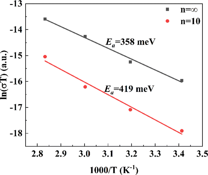
To explore the dimension regulation from the perspective of ion migration mechanisms and deeply analyze the intrinsic ion migration mechanism, the conductivity of the thick film devices was calculated based on the I–V curves in the high-temperature region. The degree of ion migration in the thick films was quantitatively analyzed using the Arrhenius equation related to temperature, with the ion migration activation energy Ea representing this characteristic. As shown in Fig. 7, for the control group n = ∞ material, upon heating to 293 K, which enters the high-temperature region, the ion conductivity dominates the total conductivity, resulting in an Ea calculated to be 358 meV, consistent with other reports. For the quasi-two-dimensional structure of n = 10 material treated with the large organic molecule n-BABr, Ea increased to 419 meV, indicating an ion migration activation energy increase of about 17%. The perovskite thick films modified with n-BABr show a significant suppression effect on ion migration, benefiting from the dimensional regulation by the large organic molecules. This effect constructs van der Waals gaps between layers, which restricts the migration of ions between layers.
 | ||
| Fig. 7 Temperature-dependent conductivity test. | ||
3.6 X-ray detection test and analysis
For X-ray response testing, ITO/PVP/perovskite/Ag devices were placed under X-Rays with a photon energy of 80 keV, testing the photo-current and dark current under different doses and biases, thereby calculating parameters such as the device's X-ray sensitivity and detection limit.The photocurrent-dose rate curves of the devices under different electric field strengths were tested and plotted as shown in Fig. 8(a). The slopes for each group were obtained using linear fitting, summarizing the X-ray sensitivity values of the devices as shown in Table 1. It was found that the device's sensitivity at an electric field strength of 20 V mm−1 was 24.27 μC Gyair−1 cm−2. To improve the device's response speed and carrier collection efficiency, applying a higher voltage under a certain dose rate of X-ray irradiation will produce a larger photo-response current, while the dark current remains stable, thereby achieving higher device sensitivity. The device approaches saturation under an electric field of 400 V mm−1, with sensitivity reaching 46.98 μC Gyair−1 cm−2, twice that of amorphous selenium X-ray detectors (20 μC Gyair−1 cm−2). Further optimization of the thick film formation and crystal quality, improving carrier mobility, and suppressing ion migration, enable the device to operate at higher electric field strengths, potentially enhancing sensitivity to a higher level.
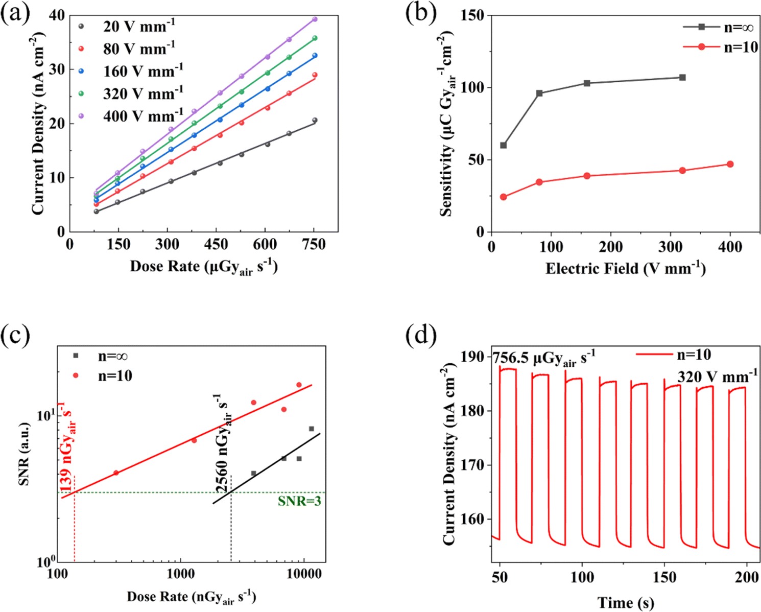 | ||
| Fig. 8 (a) Photocurrent density–dose curves of the n = 10 under different electric field; (b) summary of the sensitivities of n = 10 and n = ∞ at different electric fields; (c) signal-to-noise ratio versus X-ray dose rate for n = 10 and n = ∞, with the limit of detection obtained through linear fitting; (d) the cycle stability of n = 10 device at 320 V mm−1 electric field (8 consecutive on–off cycles). | ||
| Electric field E/V mm−1 | Sensitivity S/μC Gyair−1 cm−2 | R2 (%) |
|---|---|---|
| 20 | 24.27 | 99.72 |
| 80 | 34.54 | 99.80 |
| 160 | 38.86 | 99.92 |
| 320 | 42.59 | 99.93 |
| 400 | 46.98 | 99.91 |
For X-ray detectors, the detection limit is also an important performance metric. As shown in Fig. 8(c), detection limit testing was performed for two types of devices under an electric field of 320 V mm−1. By linear fitting of the signal-to-noise ratio for different doses, the detection limits for the two types of detectors were determined, with the n = 10 detector having a detection limit of 138 nGyair s−1, better than the n = ∞ detector's 2560 nGyair s−1. The detection limits of both types of X-ray detectors are low, with the n = 10 detector being an order of magnitude lower than commercial amorphous selenium detectors (Table S1, ESI†), sufficient to meet standard medical diagnostic requirements, and close to the detection limit of 59.7 for Cs2AgBiBr6 single crystal X-ray detectors (Table S1, ESI†), significantly reducing X-ray harm to the human body. The lower detection limit of X-ray detectors is due to lower dark current under comparable photo-current, which suppresses the device's noise current, thereby improving the signal-to-noise ratio and allowing the device to respond noticeably at smaller X-ray doses. The construction of quasi-two-dimensional structures suppresses ion migration, reducing ionic conduction and thereby achieving excellent X-ray detector performance in terms of detection limit.
Notably, the sensitivity of the device decreases after reasonable addition of n-BABr for dimension regulation of the three-dimensional perovskite, as shown in Fig. 8(b). This phenomenon can be attributed to the hindrance of organic interlayers to the transport of photogenerated carriers33 and the higher defect density and grain boundaries within the thick film affecting carrier transport. Thus, to some extent, it weakens the carrier collection efficiency, resulting in lower sensitivity compared to three-dimensional perovskite materials. In fact, compared to the significant optimization of dark current stability, this decrease in sensitivity performance is within an acceptable range.
Fig. 8(d) shows the detector's on/off cycling curve, used to test the device's cyclic stability performance. The test results indicate that the n = 10 device maintains a stable dark current baseline under high electric field and long-term testing, with a slight reduction in photo-response current. This might be due to an increase in internal defects within the thick film under high-energy X-ray irradiation, increasing the probability of carrier recombination and reducing photogenerated carriers.
4. Conclusion
In this work, a strategy of dimension regulation of lead-free perovskite three-dimensional structures using large organic molecules was adopted, and quasi-two-dimensional lead-free perovskite materials were prepared via an ultrasonic spray coating process. Thanks to the van der Waals gaps constructed by organic molecular layers, the movement of ions between perovskite layers was blocked, thereby reducing the ionic conductivity and stabilizing the device's dark and response currents. By rationally controlling the content of organic molecules, a material designated as n = 10, namely (BA)2Cs9Ag5Bi5Br31, was designed. This significantly enhanced the material's resistivity, effectively reduced dark current and current drift, increased the ion migration activation energy, and ensured long-term device stability. This provides a new perspective for the dimension regulation of lead-free polycrystalline perovskites and opens up broad prospects for their applications in X-ray detection and imaging.Data availability
The data supporting this article have been included as part of the ESI.†Conflicts of interest
There are no conflicts to declare.Acknowledgements
This work is supported by West China Hospital of Sichuan University-University of Electronic Science and Technology of China Medical and Industrial Integration Cross-Cultivation Project (ZYGX2022YGRH006), Project of Guangxi Key Laboratory of Superhard Materials (China Nonferrous Metal Guilin Research Institute of Geology for Mineral Resources) (No. 2023-K-01), the Research Foundation of Key Laboratory of New Processing Technology for Nonferrous Metal & Materials, Ministry of Education/Guangxi Key Laboratory of Optical and Electronic Materials and Devices (No. 22KF-23). The Sichuan Province Science and Technology Activities Funding for Returned Overseas Scholars. The authors also thank Shiyanjia Lab (https://www.shiyanjia.com) for the support of XRD and SEM test.References
- S.-A. Zhou and A. Brahme, Development of phase-contrast X-Ray imaging techniques and potential medical applications, Phys. Med. Eur. J. Med. Phys., 2008, 24(3), 129–148 CrossRef.
- A. Olivo, D. Chana and R. Speller, A preliminary investigation of the potential of phase contrast X-Ray imaging in the field of homeland security, J. Phys. D: Appl. Phys., 2008, 41(22), 225503 CrossRef.
- P. Fromme and J. C. H. Spence, Femtosecond nanocrystallography using X-Ray lasers for membrane protein structure determination, Curr. Opin. Struct. Biol., 2011, 21(4), 509–516 CrossRef CAS PubMed.
- T. Masuzawa, I. Saito and T. Yamada, et al., Development of an amorphous selenium-based photodetector driven by a diamond cold cathode, Sensors, 2013, 13(10), 13744–13778 CrossRef CAS PubMed.
- W. Wei, Y. Zhang and Q. Xu, et al., Monolithic integration of hybrid perovskite single crystals with heterogenous substrate for highly sensitive X-Ray imaging, Nat. Photonics, 2017, 11(5), 315–321 CrossRef CAS.
- Y. Liu, Z. Xu and Z. Yang, et al., Inch-size 0d-structured lead-free perovskite single crystals for highly sensitive stable X-Ray imaging, Matter, 2020, 3(1), 180–196 CrossRef.
- A. Raj, M. Kumar and A. Kumar, et al., Investigating the potential of lead-free double perovskite Cs2AgBiBr6 material for solar cell applications: A theoretical study, Int. J. Energy Res., 2022, 46(10), 13801–13819 CrossRef CAS.
- Z. Li, F. Zhou and H. Yao, et al., Halide perovskites for high-performance X-Ray detector, Mater. Today, 2021, 48, 155–175 CrossRef.
- T. Yang, F. Li and R. Zheng, Recent advances in radiation detection technologies enabled by metal-halide perovskites, Mater. Adv., 2021, 2(21), 6744–6767 RSC.
- H. Wei and J. Huang, Halide lead perovskites for ionizing radiation detection, Nat. Commun., 2019, 10(1), 1066 CrossRef.
- H. Wu, Y. Ge and G. Niu, et al., Metal halide perovskites for X-Ray detection and imaging, Matter, 2021, 4(1), 144–163 CrossRef CAS.
- W. Pan, H. Wu and J. Luo, et al., Cs2AgBiBr6 single-crystal X-Ray detectors with a low detection limit, Nat. Photonics, 2017, 11(11), 726–732 CrossRef CAS.
- W. Qian, X. Xu and J. Wang, et al., An aerosol-liquid-solid process for the general synthesis of halide perovskite thick films for direct-conversion X-Ray detectors, Matter, 2021, 4(3), 942–954 CrossRef CAS.
- B.-w Park and S. I. Seok, Intrinsic instability of inorganic-organic hybrid halide perovskite materials, Adv. Mater., 2019, 31(20), 1805337 CrossRef PubMed.
- H. Li, X. Shan and J. N. Neu, et al., Lead-free halide double perovskite-polymer composites for flexible X-Ray imaging, J. Mater. Chem. C, 2018, 6(44), 11961–11967 RSC.
- M. Xia, Z. Song and H. Wu, et al., Compact and large-area perovskite films achieved via soft-pressing and multi-functional polymerizable binder for flat-panel X-Ray imager, Adv. Funct. Mater., 2022, 32(16), 2110729 CrossRef CAS.
- D. Meggiolaro, E. Mosconi and F. De Angelis, Formation of surface defects dominates ion migration in lead-halide perovskites, ACS Energy Lett., 2019, 4(3), 779–785 CrossRef CAS.
- B. Yang, W. Pan and H. Wu, et al., Heteroepitaxial passivation of Cs2AgBiBr6 wafers with suppressed ionic migration for X-Ray imaging, Nat. Commun., 2019, 10, 1989 CrossRef PubMed.
- H. Tsai, S. Shrestha and L. Pan, et al., Quasi-2d perovskite crystalline layers for printable direct conversion X-Ray imaging, Adv. Mater., 2022, 34(13), 2106498 CrossRef CAS.
- Y. Li, Y. Lei and H. Wang, et al., Two-dimensional metal halides for X-Ray detection applications, Nano-Micro Lett., 2023, 15(1), 128 CrossRef CAS PubMed.
- Z. Xu, X. Liu and Y. Li, et al., Exploring lead-free hybrid double perovskite crystals of (BA)2CsAgBiBr7 with large mobility-lifetime product toward X-Ray detection, Angew. Chem., Int. Ed., 2019, 58(44), 15757–15761 CrossRef CAS PubMed.
- G. J. Yukta and M. A. Afroz, et al., Efficient and highly stable X-Ray detection and imaging using 2D (BA)2PbI4 perovskite single crystals, ACS Photonics, 2022, 9(11), 3529–3539 CrossRef.
- M. Zhang, D. Xin and S. Dong, et al., Methylamine-assisted preparation of ruddlesden-popper perovskites for stable detection and imaging of X-Rays, Adv. Opt. Mater., 2022, 10(23), 2201548 CrossRef CAS.
- X. Zhang, T. Zhu and C. Ji, et al., In situ epitaxial growth of centimeter-sized lead-free (BA)2CsAgBiBr7/Cs2AgBiBr6 heterocrystals for self-driven X-Ray detection, J. Am. Chem. Soc., 2021, 143(49), 20802–20810 CrossRef CAS PubMed.
- B. A. Connor, L. Leppert and M. D. Smith, et al., Layered halide double perovskites: Dimensional reduction of Cs2AgBiBr6, J. Am. Chem. Soc., 2018, 140(15), 5235–5240 CrossRef CAS PubMed.
- X. He, M. Xia and H. Wu, et al., Quasi-2d perovskite thick film for X-Ray detection with low detection limit, Adv. Funct. Mater., 2021, 32(7), 2109458 CrossRef.
- S. Khare and J. V. Gohel, Performance enhancement of cost-effective mixed cationic perovskite solar cell with MgCl2 and n-BAI as surface passivating agents, Opt. Mater., 2022, 132, 112845 CrossRef CAS.
- J. Gong, M. Hao and Y. Zhang, et al., Layered 2D halide perovskites beyond the Ruddlesden-Popper phase: Tailored interlayer chemistries for high-performance solar cells, Angew. Chem., Int. Ed., 2022, 61(10), e202112022 CrossRef CAS.
- Y. Miao, M. Ren and H. Wang, et al., Surface termination on unstable methylammonium-based perovskite using a steric barrier for improved perovskite solar cells, Angew. Chem.,Int. Ed., 2023, 62(51), e202312726 CrossRef CAS PubMed.
- D. He, R. Li and B. Liu, et al., Unraveling abnormal buried interface anion defect passivation mechanisms depending on cation-induced steric hindrance for efficient and stable perovskite solar cells, J. Energy Chem., 2023, 80, 1–9 CrossRef CAS.
- Z. Xiao, R. A. Kerner and L. Zhao, et al., Efficient perovskite light-emitting diodes featuring nanometre-sized crystallites, Nat. Photonics, 2017, 11(2), 108–115 CrossRef CAS.
- C. Xue, Y. Xiao and X. Liu, et al., Realizing low-ion-migration and highly sensitive X-Ray detection by building g-C3N4 and ch3nh3pbi3 bulk heterojunction pellets, J. Mater. Chem. A, 2023, 11(47), 25918–25928 RSC.
- D. Xin, M. Zhang and Z. Fan, et al., A-site cation engineering of Ruddlesden–Popper perovskites for stable, sensitive, and portable direct conversion X-Ray imaging detectors, J. Phys. Chem. Lett., 2022, 13(51), 11928–11935 CrossRef CAS PubMed.
Footnote |
| † Electronic supplementary information (ESI) available. See DOI: https://doi.org/10.1039/d4ra02606c |
| This journal is © The Royal Society of Chemistry 2024 |