
 Open Access Article
 This Open Access Article is licensed under a Creative Commons Attribution-Non Commercial 3.0 Unported Licence
Effect of TCS gas flow and pre-etching on homopitaxial growth of 4H-SiC
Ning Guo ab,
Yicheng Peia,
Weilong Yuana,
Yunkai Liab,
Siqi Zhaoab,
Shangyu Yangab,
Yang Zhang*ab and
Xingfang Liu*ab
ab,
Yicheng Peia,
Weilong Yuana,
Yunkai Liab,
Siqi Zhaoab,
Shangyu Yangab,
Yang Zhang*ab and
Xingfang Liu*ab
aKey Laboratory of Semiconductor Materials Science, Institute of Semiconductors, Chinese Academy of Sciences, Beijing 100083, People's Republic of China. E-mail: liuxf@semi.ac.cn
bCenter of Materials Science and Optoelectronics Engineering, University of Chinese Academy of Sciences, Beijing 100049, People's Republic of China. E-mail: zhang_yang@semi.ac.cn
First published on 22nd May 2024
Abstract
In this study, the epitaxial growth of 6-inch n-type 4° off-axis Si-face substrates using a horizontal hot-wall LPCVD system was investigated. The study explored the epitaxial growth under different source gas flow rates, growth pressures, and pre-etching times, with particular emphasis on their effects on epitaxial growth rate, epitaxial layer thickness uniformity, doping concentration and uniformity, and epitaxial layer surface roughness. The observation was made that the increase in source gas flow rate led to variations in dopant concentration due to different transport models between nitrogen gas and source gas. Additionally, with the increase in etching time, overetching phenomena occurred, resulting in changes in both dopant concentration and uniformity. Furthermore, the relationships between these three factors and their corresponding indicators were explained by combining the CVD growth process with the laminar flow model. These observed patterns are beneficial for further optimizing growth conditions in industrial settings, ultimately enhancing the quality of the growth process.
Introduction
Currently, most epitaxial growth processes are predominantly homoepitaxial, and the matured SiC device structures in the industry are primarily based on 4H-SiC.1–3 Consequently, the optimization of epitaxial techniques and growth processes in the industry is primarily focused on homoepitaxial growth of 4H-SiC.3,4 Previous research has shown that under conditions of significant fluctuations in source gas flow rates during epitaxial growth, especially when the magnitude of the flow rate variation is nearly equal to the magnitude of the source gas flow rate itself, there is a gradual transition of the epitaxial growth from 4H to 3C polytype as the source gas flow rate increases.5 Under specific source gas flow rate conditions, both 3C and 4H polytypes may simultaneously appear on the same epitaxial wafer. In order to determine the influence of source gas flow rates on homoepitaxial growth of 4H-SiC during homoepitaxial growth, and to provide better references for controlling the growth parameters of homoepitaxial 4H-SiC processes, it is necessary to vary experimental conditions. Specifically, under lower source gas flow rates, reducing the magnitude of fluctuations in source gas flow rates and conducting experiments on the effects of different source gas flow rates on epitaxial growth under the premise of homoepitaxial growth. Additionally, chamber pressure also affects the flow rate of the source gas, the thickness of the boundary layer,6,7 and the stability of the gas flow, thereby influencing the kinetics of epitaxial growth. Therefore, it is necessary to study the relationship between chamber pressure and the quality of gas-phase epitaxial growth.The quality of epitaxial layers depends not only on various process parameters of the chemical vapor deposition process but also significantly on the quality of the substrate.8–10 There is ample evidence from numerous studies indicating that many defects in epitaxial layers are caused by defects on the substrate surface or extensions of substrate defects.11–13 Common methods for eliminating defects in epitaxial layers caused by substrate surface defects involve treating the substrate surface to improve the quality of the epitaxial layer. For example, common substrate surface defects such as carbon inclusions and scratches can be eliminated through surface treatment. Pre-growth in situ etching with H2 is one such surface treatment process.14–16 At a certain temperature, using H2 for in situ etching can eliminate surface scratches, improve substrate surface smoothness, and enhance substrate surface quality. Importantly, through chemical reactions, a layer of SiC is removed from the surface while forming steps. The formal growth stage then involves step flow growth, where C atoms and Si atoms decomposed from the source gas molecules will adsorb and nucleate at the steps, ultimately completing the homogeneous epitaxial growth of SiC. Therefore, in situ etching is an important process for SiC homogeneous epitaxial growth.
The objective of the present research is to study the effect of epitaxial growth conditions on the epitaxial growth rate, epitaxial layer thickness uniformity, doping concentration and uniformity, and epitaxial layer surface roughness for real-life applications. In this article, particular attention is paid to the effects of three process parameters, namely source gas flow rate, growth pressure, and pre-etching time, on various growth metrics under different experimental conditions. A series of experiments were designed and conducted to investigate these influences.
Experimental
To investigate the influence of source gas flow rate on the homogeneous epitaxial growth of 4H-SiC during the epitaxial growth process and to provide better references for regulating the growth parameters of 4H-SiC homogeneous epitaxy, experiments were conducted under the premise of homogeneous epitaxy, varying the source gas flow rates to observe their effects on epitaxial growth. The experimental groups were labelled as Group A, and the experimental procedure was as follows: at an epitaxial growth temperature of 1570 °C in a horizontal hot-wall CVD system, 6-inch 4H-SiC n-type substrates were selected, and epitaxial layer growth experiments were conducted on the (0001) surface of these substrates. Trimethylsilane (TCS) diluted with H2 and ethylene (C2H4) were used as the Si and C sources, respectively. During the formal epitaxial layer growth, the C/Si ratio was controlled at 0.72, and nitrogen (N2) was used as the n-type doping source. The flow rates of different source gases and doping gases were controlled, with reduced variations compared to previous experiments, to avoid the formation of the 3C crystal structure. During flow rate control, the flow rates of each step of the source gases and doping gases were varied in the same proportion. After determining the flow rates for one group of epitaxy, the flow rates for the other two groups of source gases and doping gases were set at 0.9 times and 1.1 times those of the experimental group, respectively. Samples with flow rates set at 0.9 times, 1.0 times, and 1.1 times were labelled as A1, A2, and A3, respectively.Taking the preparation of A2 with a source gas flow rate of 1× as an example, the specific process and experimental parameters are as follows: after cleaning the epitaxial wafer, the substrate was placed into the growth furnace. Within 26 minutes, the temperature of the substrate was raised from room temperature to 1570 °C. Subsequently, a 2 minutes pre-etching process was conducted in 100 slm of H2, with the gas pressure controlled at 70 torr during substrate pre-etching. Following this, while maintaining constant temperature, hydrogen flow rate, and pressure, TCS at a flow rate of 55 sccm and C2H4 at a flow rate of 14 sccm were introduced as the Si and C sources, respectively. Additionally, N2 at a flow rate of 84 sccm was introduced as the n-type doping source for the growth of the buffer layer, which lasted for 8 minutes. After the buffer layer growth, the flow rates of TCS, C2H4, and N2 were adjusted to 55 sccm, 20 sccm, and 33.5 sccm, respectively, for the formal epitaxial layer growth. The growth duration of the formal epitaxial layer was 38 minutes. Upon completion of the growth process, the introduction of source gases was ceased, and the flow rate of H2 was maintained until the epitaxial wafer cooled to room temperature. For A1, the flow rates of TCS, C2H4, and N2 at each step were reduced to 0.9 times that of A2, while other conditions and processes remained unchanged. A3 followed the same principle.
To investigate the specific effects of chamber pressure on the final epitaxial layer, we designed Group B experiments. Using a horizontal hot-wall CVD epitaxial equipment, the chamber temperature was raised to 1570 °C within 32 minutes and maintained. The growth pressures for four samples were controlled at 40 torr, 60 torr, 70 torr, and 80 torr, respectively, and maintained constant throughout the process. The four samples were named B1, B2, B3, and B4 accordingly. Subsequently, in situ etching was conducted for 4 minutes under a hydrogen flow rate of 100 slm. Following this, TCS at a flow rate of 27 sccm, C2H4 at a flow rate of 8 sccm, and N2 at a flow rate of 70 sccm were introduced for buffer layer growth, which lasted for 7 minutes. After the buffer layer growth, TCS at a flow rate of 50 sccm, C2H4 at a flow rate of 18 sccm, and N2 at a flow rate of 46 sccm were introduced for the formal epitaxial layer growth, which lasted for 18 minutes. Upon completion of the growth process, the heating power was turned off, and hydrogen was continuously introduced until the samples cooled to room temperature for sampling. Subsequently, tests were conducted to measure the epitaxial layer thickness, doping concentration, uniformity, and surface roughness.
To investigate the final impact of the pre-etching process before growth on the epitaxial layer, we conducted Group C experiments. During the growth of the buffer layer, the flow rate of TCS used was 30 sccm, with a C/Si ratio of 0.53, and the flow rate of N2 was 80 sccm. In the formal growth phase, the flow rate of TCS used was 50 sccm, with a C/Si ratio of 0.72, and the flow rate of N2 was 60 sccm. The flow rate of H2 was maintained at 100 slm throughout the process. The parameters for this part of the experimental group were the same, while the pre-etching time before the growth of the buffer layer was set to 0 min, 1 min, 2 min, 4 min, 6 min, 9 min, and 12 min. The samples were named C1, C2, C3, C4, C5, C6, and C7, respectively.
Results and discussion
For each epitaxial wafer in every group, the epitaxial layer thickness was measured, and both the average growth rate and the uniformity of the epitaxial layer thickness were calculated. Additionally, dopant concentration and its uniformity, as well as the surface roughness (Rq), were measured. Graphs were plotted based on the different variables within each group. The uniformity was calculated as follows:
uniformity = (σX/![[X with combining macron]](https://www.rsc.org/images/entities/i_char_0058_0304.gif) ) × 100% ) × 100%
| (1) |
 | (2) |
is the mean of the data, and n is the number of data points. The formula indicates that the lower the value of uniformity, the better the uniformity of the data set.
The surface roughness of the epitaxial layer is represented by Rq:
 | (3) |
Source gas flow rate
In Group A experiments, a graph was plotted with the TCS flow rate of the formal epitaxial layer as the horizontal axis. The relationship obtained is depicted in Fig. 1. | ||
| Fig. 1 Growth rate and thickness uniformity under different source gas flow rates. | ||
From the graph, it can be observed that the growth rate is linearly related to the source gas flow rate. This relationship is quite straightforward to understand. Under the same step-flow growth mode, the growth rate of the epitaxial layer is primarily influenced by the mass transport process. At the same pressure, the boundary layer thickness remains relatively consistent, and the mass transport of the source gas is mainly affected by the concentration of the source gas in the airflow. Without reaching saturation, an increase in the source gas flow rate will correspondingly increase the concentration of the source gas in the boundary layer, resulting in a larger concentration difference between the substrate and the boundary layer. This increase in concentration difference will enhance mass transport accordingly. The linear relationship between the source gas and the epitaxial growth rate indicates that the reaction rate during CVD epitaxial growth is greater than the gas transport rate.17,18 It also indirectly suggests that under this gas flow rate, chemical reactions near the substrate are quite sufficient, without reaching saturation, implying that gas decomposition is relatively thorough.
The unevenness of the epitaxial layer thickness decreases with increasing gas flow rate. This is different from the observation in previous experiments where roughness was observed at the substrate interface and more growth defects occurred at higher gas flow rates. The reason lies in the occurrence of 3C polytype on 4H-SiC in previous experiments. The growth mode of 3C polytype involves two-dimensional nucleation rather than step-flow growth, leading to significant randomness in the arrangement of C–Si bilayers and consequently resulting in deteriorated surface morphology and increased surface defects in the epitaxial layer. However, in 4H-SiC homogeneous epitaxy, the growth mode is characterized by step-flow growth, where the arrangement of C–Si bilayers during epitaxial growth follows the combined steps of the substrate surface. Therefore, the crystal type of the epitaxial layer is controlled by the step type of the substrate surface, ensuring that growth quality issues observed in previous experiments do not occur. Microscopically, the gas flow rate has no effect on the uniformity of homogeneous epitaxial growth. However, in terms of gas flow field distribution, under constant pressure, a higher gas flow rate results in faster flow velocity. With higher gas flow velocity, the gas ejected from the outlet can maintain a longer laminar flow region,19,20 thereby improving the uniformity of the epitaxial layer thickness and reducing the unevenness.
However, the doping concentration appeared to deviate from expectations. Despite maintaining a fixed ratio of N2 to TCS flow rates at 0.61, as shown in Fig. 2, the doping concentration decreased in the final epitaxial wafers. This indicates a different scenario compared to the case where mass transport rate limits the source gas. In the epitaxial growth process of SiC, the limitation on the decomposition of N2 and its incorporation as doping atoms into SiC is governed by the chemical reaction rate. In other words, within the boundary layer, the limitation on the rate of N atoms entering the epitaxial layer arises from the decomposition rate of N2 within the boundary layer and the mechanism of N2 entering the epitaxial layer. Since the consumption rate is relatively slow, the concentration of N2 within the boundary layer does not differ much from that in the chamber environment. Without a concentration gradient, the effect of gas flow rate on doping is relatively small. The internal bond energy of N2 itself is high, and even at a high temperature of 1570 °C, the number of N atoms generated by decomposition is very limited.21 Therefore, simply increasing the flow rate of N2 does not correspondingly increase the number of doping atoms entering the substrate and thus the doping concentration. Additionally, due to the acceleration of the growth rate, the doping concentration will decrease accordingly. This is only part of the reason for the decrease in doping concentration. In the homogeneous epitaxial growth process of SiC, the mechanism of N atom doping competes for lattice positions with C atoms.22 If the concentration of C elements in the gas increases, the competitive ability of N atoms with C atoms decreases, resulting in a decrease in doping concentration. With an increase in the concentration of source gas, the concentration of C atoms within the boundary layer increases. However, N atoms are limited by the decomposition rate and do not increase correspondingly in concentration, resulting in a decrease in doping concentration.
 | ||
| Fig. 2 Doping concentration and doping uniformity under different source gas flow rates. | ||
The aforementioned changes primarily occur at the microscale level. Whether it's the decomposition of N2 or the competitive positioning of N and C atoms, these processes are independent of the location on the substrate at the macroscopic scale. Therefore, although there are changes in doping concentration, the uniformity of doping concentration remains unchanged. Thus, in this experiment, the uniformity has consistently remained at around 10%, with almost no variation.
From the relationship between source gas flow rate and substrate surface roughness, as shown in Fig. 3, it can be observed that variations in source gas flow rate within this small range did not induce changes in surface roughness. The phenomena observed in previous experiments, such as step clustering on the smooth central region of 4H-SiC, which led to changes in surface roughness, did not occur here. In other words, as long as the growth process remains within the range of step-flow growth, the roughness of the epitaxial layer will not undergo significant changes.
 | ||
| Fig. 3 Surface roughness of epitaxial layers under different source gas flow rates. | ||
When the mechanism of epitaxial growth remains unchanged, the source gas flow rate is generally proportional to the epitaxial growth rate, and the uniformity tends to improve with an increase in the source gas flow rate. Regarding doping concentration, when N2 is used as the doping source, the doping concentration tends to decrease. It is speculated that this phenomenon is related to the high stability of N2 itself and the doping mechanism involving competition between N and C atoms for lattice positions.23 However, this relationship may not hold true when other N-containing gases are used as doping sources. Additionally, the uniformity of doping concentration and surface roughness do not fluctuate significantly with changes in gas flow rate. However, all of these observations are contingent upon the epitaxial growth proceeding in the regime of step-flow homogeneous epitaxy. If the source gas flow rate is too high, leading to two-dimensional nucleation or the formation of 3C polytype, there could be a sharp decline in epitaxial quality, accompanied by a significant increase in surface roughness and an increase in surface defects.
Chamber pressure
The chamber pressure affects various aspects of epitaxial growth. In terms of growth mechanisms, pressure directly influences the following processes:24,25(1) The thickness of the boundary layer of the epitaxial layer is directly influenced by the chamber pressure. In the gas-phase CVD process, the flow velocity of gas through the chamber is high, while the flow velocity of gas near the substrate surface is close to zero, forming a slow-moving gas layer known as the boundary layer. Gas decomposition and chemical reactions often occur within this boundary layer, and the entire physical transport process of the CVD process relies on this boundary layer. The size of this boundary layer is directly controlled by pressure, and in this mechanism, pressure directly affects the physical transport process of the source gas.
(2) The flow velocity of gas is influenced by the growth pressure. With the same source gas flow rate, when the chamber pressure increases, the volume of gas expansion decreases, resulting in a slower flow velocity of the gas under the same diameter. However, the CVD chamber is not in equilibrium. The flow velocity of gas leads to an increase in the energy absorbed by the gas, resulting in more thorough gas decomposition. Some processes that are initially influenced mostly by kinetics move toward thermodynamic equilibrium over a longer period. This movement alters the actual C/Si ratio of the gas and affects the chemical reaction process.
(3) The uniformity and stability of gas flow have a direct impact on the stability and uniformity of epitaxial growth. Moreover, under the same source gas flow rate, the gas flow field in the epitaxial reactor is regulated by the chamber pressure. Therefore, the chamber pressure during epitaxial growth also influences its stability.
The relationship obtained with the chamber pressure during the growth process as the horizontal axis is depicted in Fig. 4.
 | ||
| Fig. 4 Growth rate and thickness uniformity of epitaxial growth under different pressures. | ||
The uniformity of epitaxial layer thickness did not exhibit significant changes at chamber pressures below 70 torr. However, at a chamber pressure of 80 torr, there was a notable increase in the unevenness of the growth thickness. This may be attributed to the fact that at low chamber pressures, the growth process remained relatively unchanged. However, when the chamber pressure increased to a certain extent, the increase in boundary layer thickness altered the mass transport in the epitaxial layer, resulting in significant fluctuations in the thickness at the center and edges of the substrate. Additionally, constrained by the size and diameter of the chamber, at lower air pressures, the airflow over the substrate surface did not experience turbulence. However, when the chamber pressure increased to a certain level, the interaction between the airflow and the growth chamber led to turbulence, resulting in sudden unevenness in epitaxial thickness.26
As shown in Fig. 5, the graph illustrates the variation of doping concentration and uniformity with the growth chamber pressure. The doping concentration showed no significant changes below 60 torr, but increased as the chamber pressure exceeded 60 torr. By the time the chamber pressure exceeded 80 torr, the doping concentration was approximately 50% higher compared to conditions at 40 torr. One possible factor contributing to this change is the reduction in the mean free path of molecules with changing chamber pressure, indicating that at higher chamber pressures, it takes longer for gas molecules to traverse the same chamber length. The N-type dopant used for doping in this case is N2, and because the nitrogen–nitrogen triple bond in N2 molecules is relatively stable, even at high temperatures, the rate of nitrogen gas dissociation into N atoms is not high, and the introduced N2 molecules are not fully dissociated. However, as the residence time of gas molecules in the chamber increases, the degree of nitrogen dissociation also increases, leading to an increase in the number of N atoms capable of doping. This results in an increase in the doping concentration of the final epitaxial layer.
 | ||
| Fig. 5 Doping concentration and doping uniformity of epitaxial growth under different pressures. | ||
The doping uniformity, however, did not exhibit significant changes with the variation in chamber pressure but still showed a downward trend. The uniformity decreased from 24.5% at 40 torr to 20.9% at 80 torr, with a slight improvement in uniformity. This may be because, with the gradual increase in the number of available N atoms for doping, the distribution of N atoms in the gas phase becomes more uniform. Additionally, the increase in N atom concentration in the direction of gas flow allows the N atoms depleted at the edges to be promptly replenished from the gas, reducing the difference in doping concentration between the center and the edges, thereby enhancing doping uniformity. Furthermore, the reduction in the mean free path of gas molecules and the increase in collision frequency lead to more homogeneous gas mixing within the entire chamber, contributing to the improvement in doping uniformity.
Fig. 6 depicts AFM test images of the epitaxial wafer surfaces under different growth pressures. Here, Rq represents the surface roughness of the samples, measured in nanometers (nm). The relationship between epitaxial growth pressure and surface roughness is illustrated in Fig. 7. It can be observed that as the epitaxial growth pressure increases, the surface roughness exhibits a downward trend.
 | ||
| Fig. 6 AFM images of sample surface under different growth pressures. The shading of colors in the figure represents the surface height at that location. | ||
 | ||
| Fig. 7 Surface roughness of epitaxial growth under different pressures. | ||
The surface roughness of these samples is inherently low, and there is generally little change in roughness with increasing growth pressure. However, overall, there is a trend of decreasing roughness with increasing pressure. Surface roughness is influenced by various factors. In addition to some conventional point and line defects, the most significant factor affecting surface roughness of epitaxial wafers is step bunching, especially when epitaxial growth is performed using low-angle substrates. In previous studies, researchers proposed a model explaining step motion.27,28 When atoms are adsorbed to a step, they can move upwards to the upper terrace and combine with it, or they can move downward to join the current terrace. However, the probability of atoms moving in these two directions is different. When adsorbed atoms tend to move upwards, the upper terrace expands, thereby reducing the area of the current terrace. As the area of the current terrace decreases, the number of atoms adsorbed per unit time decreases, which in turn reduces the expansion of the upper terrace, forming a negative feedback loop on the growth rate of the terrace. Consequently, the terraces tend to grow at a uniform rate. Conversely, when atoms tend to move downwards and join the current terrace, the width of the current terrace expands, allowing more atoms to be adsorbed, resulting in a faster expansion rate of the current terrace. Consequently, the area of the lower terrace decreases, slowing down the expansion, leading to a greater difference in expansion rates between adjacent terraces. This causes the upper terrace to engulf the lower terrace, forming larger terraces with a thickness of two steps. This phenomenon manifests as step bunching on a macroscopic scale. The formation of step bunching allows the release and reduction of the surface energy of the crystal, stabilizing the crystal's surface to a relatively stable state. It is speculated that the increase in roughness at low pressure is related to this factor, as previous research has shown that step bunching defects are more likely to form at low pressure.
For the phenomenon of step bunching being more prone to occur under low pressure, several reasons are conjectured as follows:29
(1) Different stacking layers require varying growth energy, hence the growth rates of different bilayer epitaxies vary. Research indicates that in 4H-SiC, the growth rates of A and B bilayers are faster compared to the C layer.30,31 In the epitaxy of 6H-SiC, the growth rate of steps conforms to the equation.32
 | (4) |
(2) Gas pressure changes can alter the reaction rates of various reactions. However, the extent to which chamber pressure affects the rate of each reaction varies. This is especially true for the dissociation of gas sources and their binding to reactants. This process, even if the input growth source gas remains unchanged and the C/Si ratio remains constant, can lead to different proportions of carbon and silicon atoms adsorbed on the substrate surface, thereby influencing the morphology of the epitaxial material. Some studies have found that in the epitaxial growth of SiC, low pressure creates a carbon-rich environment in the growth system. In such a carbon-rich environment, the surface free energy of the substrate increases. According to previous formulas, the occurrence of step bunching can reduce the surface free energy. Therefore, from an energy perspective, changes in the gas C/Si ratio resulting from decreased chamber pressure can induce the formation of more step bunching, further increasing surface roughness.
Pre-etching time
At high temperatures, H2 reacts with the surface SiC as follows:34| SiC(s) ↔ Si(l) + C(s) | (5) |
| 2C(s) + H2(g) ↔ C2H2(g) | (6) |
| Si(l) ↔ Si(g) | (7) |
There are two factors that influence in situ etching by H2: temperature and time.35 When the pre-etching temperature is not sufficiently high or the pre-etching time is insufficient, inadequate etching may occur, resulting in the incomplete removal of defects such as scratches on the substrate surface, thereby affecting the substrate's quality.36,37 More importantly, the substrate surface steps may not be fully exposed, thereby affecting the subsequent step-flow growth process. Conversely, if the pre-etching time is too long, over-etching may occur. Over-etching can result in uneven step lengths on the surface, which is detrimental to lattice replication and can adversely affect epitaxial growth.
The relationship between pre-etching time, growth rate, and epitaxial uniformity is illustrated in Fig. 8. From this graph, it can be observed that the growth rate does not vary significantly with pre-etching time. Compared to the growth rate of 21.3 μm h−1 without pre-etching, when the pre-etching time is 12 minutes, the growth rate only decreases to 19.26 μm h−1, a change of less than 5%. However, there is an overall discernible trend where the growth rate slightly decreases with longer pre-etching times. Several factors may contribute to this trend. When the pre-etching time is short, the substrate surface roughness remains relatively high, and the substrate steps are not fully exposed. Numerous defects still exist on the substrate surface, leading to epitaxial growth that tends to nucleate at these defect sites, resulting in epitaxial layers of potentially different crystallographic orientations from the substrate and non-strict step-flow growth. Under the influence of various growth factors, the epitaxial growth rate is relatively high. As the growth time increases, the substrate steps are fully exposed, and the surface roughness becomes smoother and more regular, providing better conditions for homoepitaxial growth. However, with further prolongation of the pre-etching time, over-etching of the substrate surface may occur, resulting in wider and less regular steps. Such step morphology is not conducive to step-flow epitaxial growth and may even lead to two-dimensional nucleation phenomena. Consequently, the growth rate further decreases, and the quality of the epitaxial layer may degrade.
 | ||
| Fig. 8 Growth rate and thickness uniformity of epitaxial growth under different pre-etching times. | ||
The relationship between pre-etching time and the uniformity of epitaxial thickness further confirms the proposed mechanism regarding the relationship between pre-etching time and epitaxial growth rate. As depicted in Fig. 8, the uniformity of growth improves rapidly in the initial stages with increasing pre-etching time. The degree of non-uniformity decreases significantly from 18% without pre-etching to around 3% when the pre-etching time is 2 minutes, demonstrating a pronounced effect. However, as the pre-etching time exceeds 2 minutes, the enhancement of epitaxial thickness uniformity becomes less significant with increasing pre-etching time, although the degree of non-uniformity continues to decrease gradually, reaching its best at 9 minutes. With further increases in pre-etching time, the adverse effects of over-etching become apparent, and the non-uniformity of epitaxial layer thickness does not continue to decrease; instead, it tends to increase. This indicates the occurrence of uneven step widths and two-dimensional nucleation phenomena, leading to the non-uniformity of epitaxial thickness.
Fig. 9 illustrates the relationship between etching time and doping concentration as well as doping uniformity. Similar to the relationship between etching time and epitaxial thickness, the relationship between etching time and doping concentration exhibits significant effects during the initial etching process. After 2 minutes of etching, the doping concentration decreases from the initial value of 1.35 × 1016 cm−3 to 1.08 × 1016 cm−3, with a change magnitude of nearly 20%. Subsequently, with increasing etching time, the doping concentration gradually decreases and reaches its minimum when the etching time reaches 9 minutes. However, the impact of etching time on doping concentration becomes less pronounced afterward, with the doping concentration remaining around 1.05 × 1016 cm−3, with a variation magnitude of approximately 5%. At 12 minutes of etching time, there is a slight rebound in doping concentration, although the magnitude of the rebound remains low. The manner in which N atoms, as doping atoms, enter the epitaxial layer is related to the growth mode of the epitaxial layer. When the epitaxial layer grows relatively irregularly, it is difficult for N atoms to enter the epitaxial layer. As previously analyzed, under conditions of short etching time, the epitaxial growth does not strictly follow the step-flow growth mode. Many nucleation sites are not on the terraces of the off-angle substrate but on the rough parts of the substrate surface. This nucleation mode favors the entry of N atoms, resulting in relatively high doping concentration when etching is not performed or when the etching time is short. With increasing etching time, the terraces on the substrate surface gradually become apparent, and the growth mode gradually transitions to step-flow growth. In step-flow growth, it is more difficult for N atoms to enter the crystal for doping, resulting in lower doping concentration. Similarly, when the etching time is increased to 12 minutes, the appearance of over-etching on the substrate surface also leads to the epitaxial growth becoming less regular, resulting in a slight rebound in doping concentration in the epitaxial layer.
 | ||
| Fig. 9 Doping concentration and doping uniformity under different pre-etching times. | ||
The relationship between pre-etching time and doping concentration uniformity can also be explained by the aforementioned mechanism. When the pre-etching time is short, the epitaxial nucleation sites are mainly defects on the substrate surface and rough areas of the substrate. The distribution of these defects and rough areas on the wafer surface is not uniform, leading to different epitaxial growth rates at different locations on the substrate surface. The variation in epitaxial growth rates results in different doping concentrations, leading to doping concentration non-uniformity. As the pre-etching time increases, the terraces on the substrate surface gradually become apparent. At this point, the epitaxial growth mechanism transitions to step-flow growth. Since the terraces at various locations on the substrate are essentially the same, the rates of adsorption, migration, and incorporation of atoms on the terraces are almost identical. Consequently, the process of N atom incorporation and binding becomes more stable, resulting in similar doping rates at various locations on the wafer and thus similar doping concentrations. The epitaxial non-uniformity is minimized at this stage. However, when the pre-etching time continues to increase to the point of over-etching, the terraces on the substrate surface are no longer uniformly etched. Consequently, the epitaxial growth mode and rates vary at different locations, leading to differences in epitaxial growth rates. Under these conditions, the doping rates at each location also differ, resulting in doping concentration non-uniformity.
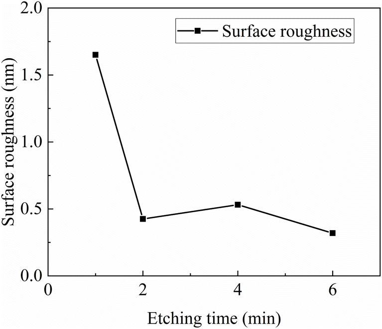
We selected samples with pre-etching times of 1 min, 2 min, 4 min, and 6 min for surface roughness testing. The AFM images of the sample test results are shown in Fig. 10, and the relationship between sample roughness and pre-etching time is presented in Fig. 11. From this figure, it can be observed that with increasing pre-etching time, the surface roughness exhibits a trend of initially decreasing and then gradually stabilizing, which is in line with expectations. This trend arises because at lower pre-etching times, as the pre-etching time increases, the substrate surface becomes smoother and the substrate terraces gradually become apparent. Additionally, with increasing pre-etching time, the substrate surface becomes progressively smoother. Furthermore, within these pre-etching time ranges, the substrate surface does not exhibit signs of over-etching. Conducting homoepitaxial growth in step-flow mode is a relatively stable growth mode, and thus, the roughness of the substrate essentially determines the roughness of the epitaxial layer. Consequently, the roughness of the epitaxial layer continues to decrease. For pre-etching times beyond one minute, the substrate terraces are exposed, and before over-etching occurs, the substrate roughness remains unchanged. Therefore, the roughness of the epitaxial layer for these samples is essentially the same.
 | ||
| Fig. 10 AFM images of sample surface under different pre-etching times. The shading of colors in the figure represents the surface height at that location. | ||
 | ||
| Fig. 11 Surface roughness under different pre-etching times. | ||
Conclusions
In summary, we conducted SiC epitaxial experiments on 6-inch n-type substrates with a 4° off-axis orientation. By controlling process parameters such as source gas flow rate, chamber pressure, and pre-etching time, we investigated the relationship between these parameters and the quality of the epitaxial layer. Our focus in evaluating epitaxial quality included parameters such as epitaxial growth rate, thickness uniformity, doping concentration, uniformity of doping concentration, and surface roughness of the epitaxial layer.In scenarios where the variation in source gas flow rate is minimal, distinct epitaxial outcomes were observed under the same growth system and process conditions. Under minor changes in source gas flow rate, the epitaxial growth mode remained unchanged, preserving homogeneous epitaxy. The epitaxial growth rate exhibited a linear increase with the source gas flow rate, while the uniformity of epitaxial layer thickness improved with increasing flow rate. However, no significant correlation was observed between the surface roughness of the epitaxial layer and the source gas flow rate. Conversely, the doping concentration decreased with increasing source gas flow rate, although the uniformity of doping concentration did not exhibit noticeable variations.
As the growth pressure gradually increased, a slight decrease in growth rate was observed, while the unevenness of epitaxial layer thickness remained relatively unchanged under low-pressure conditions, but increased under high-pressure conditions. The doping concentration increased with the rise in gas pressure, leading to a more uniform distribution of doping concentration. Additionally, the reduction in defects caused by step clustering under low pressure resulted in a decrease in the surface roughness of the epitaxial layer.
The pre-etching time has minimal impact on the epitaxial growth rate, but it generally exhibits a slight decrease as the pre-etching time prolongs. Moreover, an increase in pre-etching time leads to a reduction in substrate surface roughness and an improvement in the uniformity of epitaxial layer thickness. However, with further increase in pre-etching time leading to over-etching, the thickness uniformity deteriorates. Similarly, the doping concentration and its uniformity show a similar trend with increasing pre-etching time.
Author contributions
Data curation, methodology, formal analysis, writing – original draft preparation, Ning Guo; software, visualization, validation, Yicheng Pei; investigation, formal analysis, Weilong Yuan; methodology, Shangyu Yang; software, visualization, Siqi Zhao; supervision, resources, investigation, Yunkai Li; project administration, investigation, supervision, Yang Zhang; conceptualization, supervision, funding acquisition, writing – review and editing, Xingfang Liu. All authors have read and agreed to the published version of the manuscript.Conflicts of interest
There are no conflicts to declare.Acknowledgements
This work was supported by the Key-Area Research and Development Program of Guangdong Province (Grant No. 2021B0101300005), the National Key R&D Program of China (Grant No. 2021YFB3401603), and the National Natural Science Foundation of China (No. 12175236).Notes and references
- H. Zhang, H. Zhang, Q. Jia, C. Yin, Z. Deng, W. Guo and Z. Wan, IEEE Trans. Compon., Packag., Manuf. Technol., 2023, 13, 897–905 CAS.
- E. A. Panyutin, S. S. Sharofidinov, T. A. Orlova, S. A. Snytkina and A. A. Lebedev, Tech. Phys., 2020, 65, 428–433 CrossRef CAS.
- J. Ul Hassan, R. Karhu, L. Lilja and E. Janzen, Cryst. Growth Des., 2019, 19, 3288–3297 CrossRef CAS.
- W. Yuan, Y. Pei, N. Guo, Y. Li, X. Zhang and X. Liu, Crystals, 2023, 13, 935 CrossRef CAS.
- N. Guo, Y. Pei, W. Yuan, Y. Li, S. Zhao, S. Yang, Y. Zhang and X. Liu, Crystals, 2023, 13, 1123 CrossRef CAS.
- K. Petroski, S. Poges, C. Monteleone, J. Grady, R. Bhatt and S. L. Suib, ACS Appl. Mater. Interfaces, 2018, 10, 4986–4992 CrossRef CAS PubMed.
- I. Peivaste, G. Alahyarizadeh, A. Minuchehr and M. Aghaie, Vacuum, 2018, 154, 37–43 CrossRef CAS.
- J. a. Kong, Y. Zhang, W. Gai, G. Chen, Y. Lin, H. Wang and H. Li, J. Eur. Ceram. Soc., 2024, 44, 68–78 CrossRef CAS.
- L. Tang and C. Dames, J. Appl. Phys., 2023, 134, 165101 CrossRef CAS.
- D. Kim, D. Y. Kim, J. H. Kwon, K.-S. Kim and N.-M. Hwang, Electron. Mater. Lett., 2020, 16, 498–505 CrossRef CAS.
- Y. Song, N. Yang, H. Li, W. Wang and X. Chen, Cryst. Growth Des., 2023, 23, 7440–7447 CrossRef CAS.
- P. C. Chen, W. C. Miao, T. Ahmed, Y. Y. Pan, C. L. Lin, S. C. Chen, H. C. Kuo, B. Y. Tsui and D. H. Lien, Nanoscale Res. Lett., 2022, 17, 30 CrossRef PubMed.
- A. Patel, M. Mittal, D. V. S. Rao, A. K. Garg, R. Tyagi and O. P. Thakur, J. Mater. Sci.: Mater. Electron., 2021, 32, 2187–2192 CrossRef CAS.
- K. M. Chahrour and M. R. Hashim, Appl. Phys., 2020, 126, 539 CAS.
- W. Geng, G. Yang, X. Zhang, X. Zhang, Y. Wang, L. Song, P. Chen, Y. Zhang, X. Pi and D. Yang, J. Semicond., 2022, 43, 102801 CrossRef CAS.
- S. Whiteley, A. Sorensen, J. J. Vajo, R. Sfadia, T. D. Ladd, S. Cui and J. Graetz, J. Electrochem. Soc., 2023, 170, 036508 CrossRef CAS.
- P.J. Lu, W. Huang, J.J. Wang, H.T. Yang, S.Y. Guo, B. Li, T. Wang, C.T.F. Zhang, R. Tu and S. Zhang, J. Cryst. Growth, 2024, 626, 127489 CrossRef CAS.
- S.-i. Nishizawa and M. Pons, Microelectron. Eng., 2006, 83, 100–103 CrossRef CAS.
- Q.-G. Fu, H.-J. Li, X.-H. Shi, K.-Z. Li, J. Wei and Z.-B. Hu, Mater. Chem. Phys., 2006, 100, 108–111 CrossRef CAS.
- K. Wada, T. Kimoto, K. Nishikawa and H. Matsunami, Mater. Sci. Forum, 2005, 483–485, 85–88 CAS.
- G. Ferro, Crit. Rev. Solid State Mater. Sci., 2022, 47, 520–537 CrossRef CAS.
- C. G. Rodrigues, Semiconductors, 2021, 55, 625–632 CrossRef.
- U. Forsberg, Ö. Danielsson, A. Henry, M. K. Linnarsson and E. Janzén, J. Cryst. Growth, 2002, 236, 101–112 CrossRef CAS.
- M. Itoh, J. Phys. Soc. Jpn., 2020, 89, 104602 CrossRef.
- F. Triendl, G. Pfusterschmied, G. Pobegen, S. Schwarz, W. Artner, J. Konrath and U. Schmid, Mater. Sci. Semicond. Process., 2021, 131, 105888 CrossRef CAS.
- M. Kollmuss, F. La Via and P. J. Wellmann, Cryst. Res. Technol., 2023, 58, 2300034 CrossRef CAS.
- R. Sakakibara, J. Bao, K. Yuhara, K. Matsuda, T.-o. Terasawa, M. Kusunoki and W. Norimatsu, Appl. Phys. Lett., 2023, 123, 031603 CrossRef CAS.
- M. Arzig, U. Künecke, M. Salamon, N. Uhlmann and P. J. Wellmann, J. Cryst. Growth, 2021, 576, 126361 CrossRef CAS.
- J. Nishio, A. Okada, C. Ota and R. Iijima, Jpn. J. Appl. Phys., 2021, 60, SBBD01 CrossRef CAS.
- T. Ogawa, K. Fukumoto, H. Machida and K. Norinaga, Heliyon, 2023, 9, e15061 CrossRef CAS PubMed.
- X. J. Chen and Y. Li, Surf. Sci., 2019, 681, 18–23 CrossRef CAS.
- T. Kimoto and H. Matsunami, J. Appl. Phys., 1995, 78, 3132–3137 CrossRef CAS.
- X. Zheng, Y. Liu, Y. Cao, J. Wang and Y. Zhang, Ceram. Int., 2021, 47, 16162–16169 CrossRef CAS.
- A. Boukezzata, H. Menari and S. Kaci, Acta Phys. Pol., A, 2020, 137, 454–457 CrossRef CAS.
- P. Pal, S. Kumar and S. K. Singh, Def. Sci. J., 2020, 70, 515–519 CrossRef CAS.
- J. L. Weyher, A. Tiberj, G. Nowak, J. C. Culbertson and J. A. Freitas Jr, J. Electron. Mater., 2023, 52, 5039–5046 CrossRef CAS.
- J. Yu, X. Yang, Y. Peng, X. Hu, X. Wang, X. Chen and X. Xu, Crystengcomm, 2021, 23, 353–359 RSC.
| This journal is © The Royal Society of Chemistry 2024 |