
 Open Access Article
 This Open Access Article is licensed under a Creative Commons Attribution-Non Commercial 3.0 Unported Licence
Electrically tunable on-chip quantum Deutsch–Jozsa algorithm with lithium niobate metasurfaces
Haoyu Li†
ab,
Ruisheng Yang† *abc,
Yinan Zhangd,
Linyuan Douab,
Yijie Luoab,
Haigang Liangab,
Yuancheng Fane and
Zeyong Wei*abc
*abc,
Yinan Zhangd,
Linyuan Douab,
Yijie Luoab,
Haigang Liangab,
Yuancheng Fane and
Zeyong Wei*abc
aInstitute of Precision Optical Engineering, School of Physics Science and Engineering, Tongji University, Shanghai 200092, China. E-mail: rsyang@tongji.edu.cn; weizeyong@tongji.edu.cn
bMOE Key Laboratory of Advanced Micro-Structured Materials, Shanghai 200092, China
cShanghai Frontiers Science Research Base of Digital Optics, Tongji University, Shanghai 200092, China
dInstitute of Photonic Chips, University of Shanghai for Science and Technology, Shanghai, 200093, China
eKey Laboratory of Light Field Manipulation and Information Acquisition, Ministry of Industry and Information Technology and School of Physical Science and Technology, Northwestern Polytechnical University, Xi'an 710129, China
First published on 7th June 2024
Abstract
Owing to the inherent advantages of parallelism, rapid processing speed, and minimal energy consumption, optical analog computing has witnessed a progressive development. Quantum optical computing exceeds the capabilities of classical computing in terms of computational speed in numerous tasks. However, existing metamaterial-based quantum Deutsch–Jozsa (DJ) algorithm devices have large structural dimensions and are not suitable for miniaturized optical computing systems. Furthermore, most reported on-chip metasurface devices, rendered monofunctional after fabrication, do not possess sophisticated optical systems. In this work, we develop an electrically tunable on-chip DJ algorithm device on a lithium-niobate-on-insulator (LNOI) platform. The on-chip device consists of various etched slots, each with carefully designed size. By applying different external voltages to each individual unit, precise phase redistribution across the device is attainable, enabling the realization of tunable DJ algorithm. Notably, we can determine whether the oracle metasurface yields a constant or balance function by measuring the output electric field. The on-chip device is miniaturized and easy to integrate while enabling functional reconfiguration, which paves the way for numerous applications in optical computing.
1. Introduction
Exploiting the inherent properties of light, such as amplitude and phase, and the interaction between light and optical devices, optical analog computing demonstrates the capability to execute specific computational tasks. Compared to traditional digital computation, optical analog computing holds the promise of high-speed parallel information processing, attracting significant attention.1–3 Silva et al. (2014) introduced the concept of “computational metamaterials”, which are metamaterials with locally tailored electromagnetic parameters to change the waveform of the input signal.4 By harnessing the concept of computational metamaterials, researchers have achieved various optical operations, such as differentiation,5 integration,6,7 convolution,8 equation solving,9 and imaging processing,10,11 by freely manipulating the amplitude and phase of light waves. However, most existing optical computing systems employing metamaterials operate in free space, thereby restricting their integration and miniaturization.12–16 Interest in chip-level integrated analog optical computing systems is rapidly growing.17–19 Several fabrication schemes have been proposed for different types of on-chip devices, including differentiators,20 convolvers,21 and integrators.22Based on the classical mathematical operations, optical implementation of quantum algorithms has attracted the attention of researchers. Compared to qubit, photon has longer decoherence times which make it easier to manipulate. Classical optics and quantum mechanics possess shared inherent properties, including the superposition principle and interference effects, enabling the use of classical light to simulate specific quantum algorithms.23–25
Quantum algorithms exploit quantum mechanical properties such as quantum coherence,26 quantum superposition,27 quantum parallelism,28 and wavefunction collapse, thereby significantly improving the computational efficiency.29 The first quantum algorithm, Deutsch–Jozsa algorithm (DJ algorithm),30,31 was proposed by David Deutsch in 1985. Compared to classical algorithms, the DJ algorithm highlighted the significant acceleration potential inherent in quantum computing. Several practical quantum algorithms, including the Shor's algorithm32 and the quantum search algorithm,33 have been developed based on the DJ algorithm. However, current metamaterial-based DJ algorithm systems have large structural dimensions that hinder the miniaturization and integration.23,34 Moreover, the majority of metasurface devices are composed of passive building blocks, lacking tunable or reconfigurable responses.35–38 Hence, once fabricated, they are functionally fixed and incapable of being reconfigured, limiting their practical applications. Therefore, it is highly desirable to further advance the development of optical analog computing techniques.
Here, we present a lithium-niobate-on-insulator (LNOI)-based on-chip device for electrically tunable DJ algorithm, by employing the Pockels effect of lithium niobate (LN).39–43 The LNOI on-chip device consists of variously structured etched slots, each with carefully designed widths and lengths that determine the local transmission and phase shifts. By applying different external voltages to each individual unit via two gates, it is possible to alter the refractive index of LN, facilitating a precise phase redistribution across the device. This enables the implementation of an electrically tunable on-chip DJ algorithm. In this way, the type of the marked function can be distinguished through only one output electric field measurement. The proposed electrically tunable LNOI metasurface facilitates the implementation of an on-chip DJ algorithm, presenting significant potential applications such as massive matrix operations, artificial intelligence, and quantum information processing.
2. Materials and methods
Consider a function f(x) defined on {0,1}n that satisfies f(x)∈{0,1}n and the output of f(x) is divided into two cases. One is that it only outputs 0 or 1 for any input, which we call a constant function; the other is that it outputs 0 for exactly half of the inputs and 1 for the other half, which we call a balance function. For an unknown f(x), the DJ algorithm can help us distinguish between a constant function and a balance function. If we use classical computation, we need to check the outputs one by one. The worst scenario requires 2n−1 + 1 calculations if we want to get an accurate and error-free judgment. However, if we adopt the DJ algorithm, through the quantum superposition principle and interference effects, only one calculation is required for the same problem to arrive at a result.The schematic diagram of the LN-based on-chip device for tunable DJ algorithm is shown in Fig. 1. In a practical device, we can integrate the ITO electrodes into the top and bottom sides of the LN layer and applied external voltage by bonding wires on the side of the ITO, to stimulate the Pockels effect.41 Leveraging the Pockels effect of LN, the conversion between constant and balance functions can be achieved through the realization of desired phase distributions. The electric field amplitude “E(y)” of the incident wave is equivalent to the probability amplitude of the corresponding quantum state, and the spatial position “y” indexes the items in the database.24 In this work, we design an on-chip rectangular waveguide with the thickness of h = 300 nm by etching a rectangular slot in the centre of each unit of the LN layer. The on-chip DJ algorithm device comprises two intricately designed metasurfaces: an oracle metasurface and a metalens, each with 29 etched slots. According to the value of the function f, we achieve the refractive index of the oracle metasurface by designing a phase distribution φ1 of 0 and π, as shown in eqn (1),
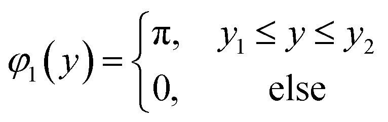 | (1) |
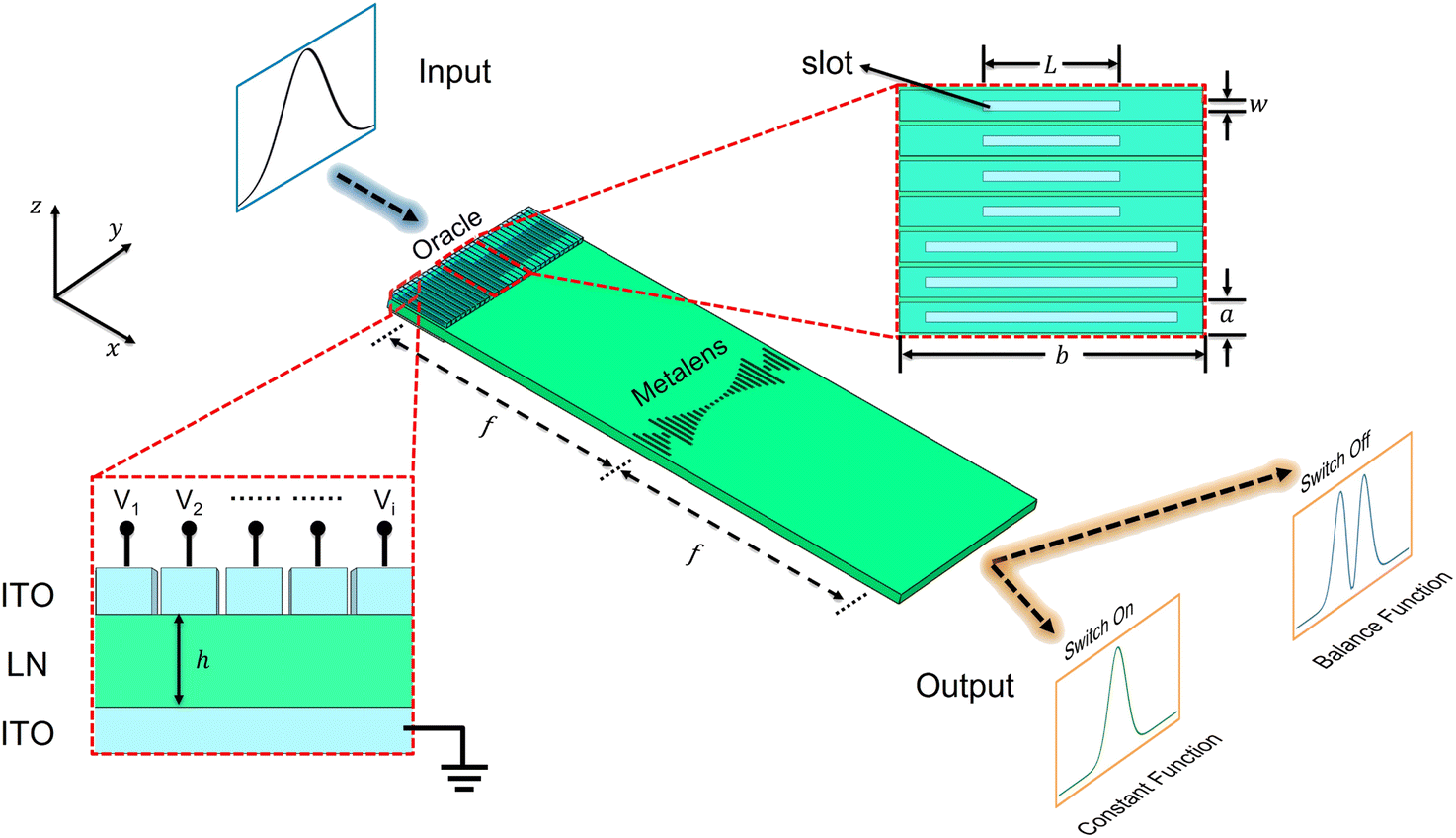 | ||
| Fig. 1 Schematic diagram of the LNOI-based on-chip device for the electrically tunable DJ algorithm. The designed on-chip structure consists of two metasurfaces: an oracle metasurface, which applies a phase shift to encode the detection function f(y); and a metalens that serves as a Fourier transformer. The function type is revealed by the output contour. Inset: the corresponding on-chip structure. a = 700 nm and b = 6000 nm denote the width and length of a unit structure, respectively. L and w represent the width and length of the slot in a unit structure, respectively. h = 300 nm is the thickness of the LN slab. f = 25 μm denotes the focal length of the metalens. | ||
We apply the Fourier transform, which is analogous to the Hadamard transform, to classical optical systems to obtain the final output signal. When the detection function is constant, the additional phase coefficients assigned by the first metasurface are equal, and the incident wave is focused on the focal plane. As for the balance function, however, the modulated wavefronts have regions of 0 and π phases shift with equal areas, which cause destructive interference with each other. Therefore, we can discern the category of the function f by measuring the spatial distribution of the electric field on the output plane. We employ an on-chip metalens in the system to implement Fourier transform. The metalens comprises an array of rectangular slots with different lengths, designed to impart a spatially-dependent phase shift along the y direction under TE incident light. The phase shift φ2 is defined by eqn (2),20
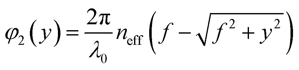 | (2) |
In our research, the oracle metasurface consists of a rectangular array of etched slots and is based on a LNOI platform. The refractive index of silica at the target wavelength λ = 1550 nm is n = 1.46 and we chose z-cut LN material (refractive index nxx = nyy = no = 2.211, nzz = ne = 2.138 at λ = 1550 nm).44 To design a high-performance beam modulation device, we first scan the width and length of the unit structure. In order to simultaneously ensure an efficient wave transmission and full phase coverage modulation, we fix the thickness of the slot to be h = 300 nm. In these simulations, we apply the periodic boundaries to the y-direction and the perfectly matched layer (PML) boundaries to the other directions. The change in refractive index of the z-cut birefringent material LN with an external voltage can be expressed as follows,45
| Δnii = −0.5riiznii3Ez | (3) |
By varying the slots width and length, we can control the transmission and the phase shift, as shown in Fig. 2(a) and (b). The transmission varies considerably when increasing the width (w) of the etching slot. By employing wider slots, we can achieve a 2π phase shift with smaller variations in slot length, however, the transmission also decreases significantly. With a slot width of w = 200 nm, the unit structure can maintain a transmission above 55%. Fig. 2(c) shows the simulated phase shift (blue curve) and transmission (orange curve) as a function of the slot length L from 0 to 5 μm. By fixing the slot width to be 200 nm, we can simultaneously achieve a phase shift from 0 to 2π and an overall transmission larger than 70%.
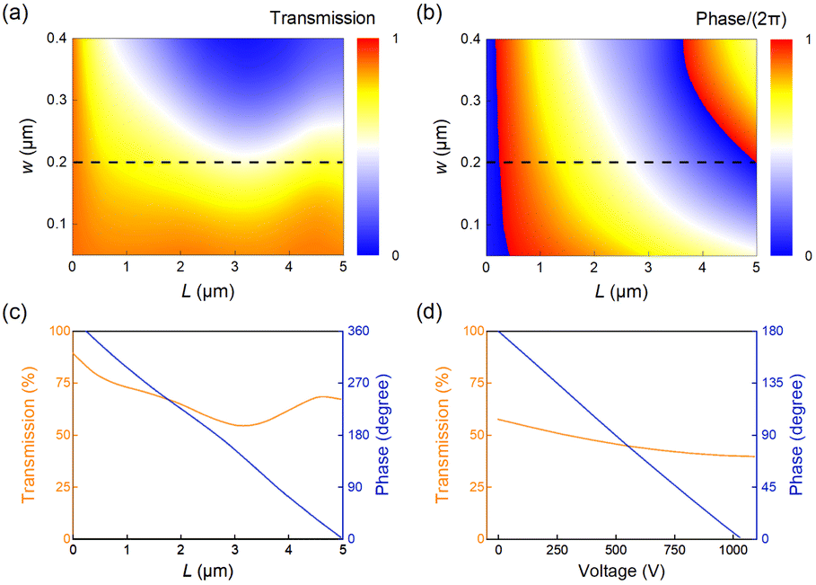 | ||
| Fig. 2 Design of on-chip unit structure. Simulated (a) transmission and (b) phase shift of the device unit structure as a function of L and w. The black dashed lines represent the parameter w = 200 nm. (c) Simulated transmission (orange curve) and phase shift (blue curve) versus slot length L, with w = 200 nm. (d) Simulated transmission (orange curve) and phase shift (blue curve) with voltage from 0 to 1100 V, with L = 2714.5 nm, w = 200 nm. | ||
It is worth noting that the phase shift is 0 when L = 5000 nm and π when L = 2714.5 nm, which is essential for DJ algorithm according to eqn (1). According to the Pockels effect eqn (3) for LN, the ordinary refractive index no decreases by a deviation Δno when different negative z-axis voltages are applied. Required for Δno = −0.20, the electric field strength is about 0.00366 V m−1 and the voltage is about 1097.07 V below the z-axis. Fig. 2(d) shows the simulated phase shift and transmission with applied voltage from 0 to 1100 V, when L = 2714.5 nm and w = 200 nm. The phase shift decreases almost linearly with increasing voltage, while the transmission is all above 40%. Note that the phase shift changes from π to 0 when Δno = −0.189, no = 2.022, ne = 1.607, Vi = 1036.73 V.
3. Results and discussion
Based on the parameters sweeping database, we determined the on-chip slot width (w = 200 nm) which guaranteed a full 0–2π phase shift over a suitable length range. Based on finite-difference-time-domain method (WGallop), we perform numerical simulations of the oracle metasurface, metalens, and the meta-systems. We apply the PML boundary conditions in all directions with an input function of E(y) = exp(−y2/20).The on-chip oracle metasurface is designed to implement a tuanble DJ algorithm on the chip device, as shown in Fig. 3(a). In eqn (1), we obtain the etched slots length to the phase distributions. The slots length at the position with a π-phase shift transition (from y1 = −0.35 μm to y2 = 10.15 μm) is 2.7145 μm, and the slots length at the position with a 0-phase shift is 5 μm.
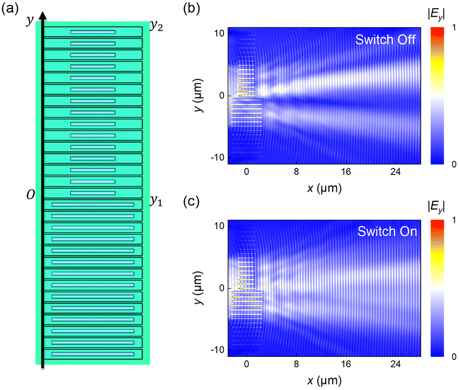 | ||
| Fig. 3 Simulated results of the oracle metasurface. (a) Schematic structure of the oracle metasurface. The electric field distribution |Ey| in LN layer, when the applied voltage is (b) switch off, and (c) switch on. | ||
Fig. 3(b) and (c) show the snapshots of the electric field intensity throughout the oracle metasurface when the external voltage is applied or not, respectively, with an input function of E(y) = exp(−y2/20). When no voltage is applied, since the length with a phase shift of π is the same as that with a phase shift of 0, the wavefront is characterized by a balance function, as shown in Fig. 3(b). As for constant function, uniform phase shift along the y-axis should be provided by the oracle metasurface. In this work, 0 is chosen to be the identical phase factor. Then we consider applying voltage to the meta-atoms. Due to the Pockels effect of the LN layer, the phase in the y1 < y < y2 region can be transformed from π to 0 when we apply the voltage Vi = 1036.73 V, as shown in Fig. 3(c). In this case, the same 0-phase shift is provided by the oracle metasurface, which means the transformation from the balance function to the constant function.
To facilitate parallel acceleration, we then apply the Fourier transform with an on-chip metalens. Therefore, we constructed an on-chip system to perform the DJ algorithm by combining oracle metasurface and metalens together. In this way, the electric field passing through the oracle metasurface will be Fourier transformed by the metalens.
Fig. 4 shows the electric field distributions across the on-chip system when the external voltage is applied or not, respectively. When there is no voltage applied (Vi = 0 V), the normalized xy-plane electric field, yz-plane electric field and the corresponding output profile are shown in Fig. 4(a)–(c) respectively. The device performs a DJ algorithm, and the central electric field is zero, which means that the on-chip oracle metasurface implements a balance function. Note that the output electric field is not symmetric in Fig. 4(c), since the effective permittivities of 0-phase and π-phase components in the device are different, which results in different transmission for the etched slots. When external voltages (Vi = 1036.73 V) are applied in the y1 < y < y2 region, the function of the oracle metasurface can be changed from the balance function to the constant function, as shown in Fig. 4(d)–(f). It can be seen that the transmitted wave is mainly concentrated at the middle part of the output port. The zero position (y = 0) has the maximum intensity, indicating that the oracle metasurface implements a constant function.
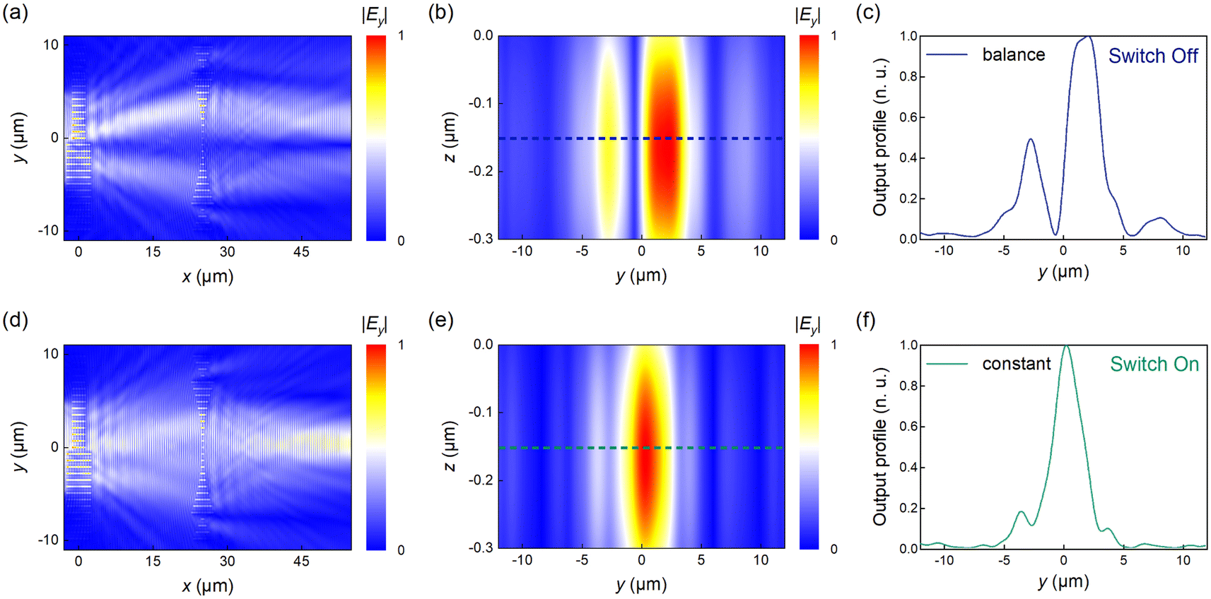 | ||
| Fig. 4 Simulated results of the actual structure for the LNOI-based on-chip device for tunable DJ algorithm when illuminated by a Gaussian profile incident wave. The xy-plane electric field distribution |Ey|, when the applied voltage is (a) switch off, and (d) switch on, respectively. The output yz-plane electric field distribution |Ey|, when the applied voltage is (b) switch off, and (e) switch on, respectively. The output profile intensity |Ey|2, when the applied voltage is (c) switch off, and (f) switch on. | ||
4. Conclusions
In summary, we propose a LNOI-based on-chip device designed to realize electrically tunable DJ algorithm, leveraging the remarkable phase modulation capabilities of LN by applying different external voltages to each individual unit via dual gates. Our results attest that the on-chip quantum DJ algorithm device can precisely determine the type of function f with only a single measurement. This work further extends the application of on-chip metasurfaces in classical optical analog computing. It also paves the way for future research on programmable or reconfigurable on-chip optical computing systems.Author contributions
Haoyu Li: conceptualization, software, data curation, methodology, validation, writing–original draft. Ruisheng Yang: supervision, validation, writing–review and editing. Yinan Zhang: validation, writing–review and editing. Linyuan Dou: methodology, writing–review and editing. Yijie Luo: writing–review and editing. Haigang Liang: writing–review and editing. Yuancheng Fan: validation, writing–review and editing. Zeyong Wei: supervision; funding acquisition; review and editing.Conflicts of interest
There are no conflicts to declare.Acknowledgements
This work is supported by the National Key Research and Development Program of China (2022YFF0604802), Shanghai Municipal Science and Technology Major Project, the Program for Professor of Special Appointment (Eastern Scholar) at Shanghai Institutions of Higher Learning, National Natural Science Foundation of China (No. 62175154), Shanghai Science and Technology Program (No. 21ZR1445500).References
- C.-W. Qiu, T. Zhang, G. Hu and Y. Kivshar, Nano Lett., 2021, 21, 5461–5474 CrossRef CAS PubMed.
- D. R. Solli and B. Jalali, Nat. Photonics, 2015, 9, 704–706 CrossRef CAS.
- A. Sajjad, H. Omid and A. Adibi, Nanophotonics, 2020, 9, 4075–4095 Search PubMed.
- A. Silva, F. Monticone, G. Castaldi, V. Galdi, A. Alù and N. Engheta, Science, 2014, 343, 160–163 CrossRef CAS.
- T. Zhu, Y. Zhou, Y. Lou, H. Ye, M. Qiu, Z. Ruan and S. Fan, Nat. Commun., 2017, 8, 15391 CrossRef CAS.
- D. A. Bykov, L. L. Doskolovich, E. A. Bezus and V. A. Soifer, Opt. Express, 2014, 22, 25084–25092 CrossRef PubMed.
- Z. Ruan, Opt. Lett., 2015, 40, 601–604 CrossRef PubMed.
- J. Cheng, V. Sitzmann, X. Dun, W. Heidrich and G. Wetzstein, Sci. Rep., 2018, 8, 12324 CrossRef PubMed.
- N. M. Estakhri, B. Edwards and N. Engheta, Science, 2019, 363, 1333–1338 CrossRef PubMed.
- Z. Wang, G. Hu, X. Wang, X. Ding, K. Zhang, H. Li, S. N. Burokur, Q. Wu, J. Liu, J. Tan and C.-W. Qiu, Nat. Commun., 2022, 13, 2188 CrossRef CAS PubMed.
- S. He, R. Wang and H. Luo, Nanophotonics, 2022, 11, 1083–1108 CrossRef CAS.
- N. Yu, P. Genevet, M. A. Kats, F. Aieta, J.-P. Tetienne, F. Capasso and Z. Gaburro, Science, 2011, 334, 333–337 CrossRef CAS PubMed.
- Z.-N. Farzad, D. L. Sounas, A. Alù and R. Fleury, Nat. Rev. Mater., 2021, 6, 207–225 Search PubMed.
- Y. Shi, Q. Song, I. Toftul, T. Zhu, Y. Yu, W. Zhu, D. P. Tsai, Y. Kivshar and A. Q. Liu, Appl. Phys. Rev., 2022, 9, 031303 CAS.
- S. Yin, E. Galiffi and A. Alù, eLight, 2022, 2, 8 CrossRef.
- A. Pors, M. G. Nielsen and S. I. Bozhevolnyi, Nano Lett., 2015, 15, 791–797 CrossRef CAS PubMed.
- H. Zhu, J. Zou, H. Zhang, Y. Shi, S. Luo, N. Wang, H. Cai, L. Wan, B. Wang, X. Jiang, J. Thompson, X. Luo, X. Zhou, L. Xiao, W. Huang, L. Patrick, M. Gu, L. C. Kwek and A. Q. Liu, Nat. Commun., 2022, 13, 1044 CrossRef CAS PubMed.
- L. L. Doskolovich, E. A. Bezus, D. A. Bykov and V. A. Soifer, J. Opt., 2016, 18, 115006 CrossRef.
- L. Li, H. Zhao, C. Liu, L. Li and T. J. Cui, eLight, 2022, 2, 7 CrossRef.
- Z. Wang, T. Li, A. Soman, D. Mao, T. Kananen and T. Gu, Nat. Commun., 2019, 10, 3547 CrossRef PubMed.
- K. Liao, T. Gan, X. Hu and Q. Gong, Nanophotonics, 2020, 9, 3315–3322 CrossRef CAS.
- C. Chen, W. Qi, Y. Yu and X. Zhang, Nanophotonics, 2021, 10, 2481–2486 CrossRef.
- K. Cheng, W. Zhang, Z. Wei, Y. Fan, C. Xu, C. Wu, X. Zhang and H. Li, Opt. Express, 2020, 28, 16230–16243 CrossRef CAS PubMed.
- W. Zhang, K. Cheng, C. Wu, Y. Wang, H. Li and X. Zhang, Adv. Mater., 2018, 30, 1703986 CrossRef.
- Z. Wei, H. Li, L. Dou, L. Xie, Z. Wang and X. Cheng, Micromachines, 2022, 13, 1204 CrossRef PubMed.
- Z. Xi, Y. Li and H. Fan, Sci. Rep., 2015, 5, 10922 CrossRef CAS PubMed.
- T. Kovachy, P. Asenbaum, C. Overstreet, C. A. Donnelly, S. M. Dickerson, A. Sugarbaker, J. M. Hogan and M. A. Kasevich, Nature, 2015, 528, 530–533 CrossRef CAS PubMed.
- F. Borjans, X. G. Croot, X. Mi, M. J. Gullans and J. R. Petta, Nature, 2020, 577, 195–198 CrossRef CAS PubMed.
- M. A. Nielsen and I. L. Chuang, Phys. Today, 2001, 54, 60 Search PubMed.
- D. Deutsch, Proc. R. Soc. A, 1985, 400, 97–117 Search PubMed.
- D. Deutsch and R. Jozsa, Proc. R. Soc. A, 1992, 439, 553–558 Search PubMed.
- T. Monz, D. Nigg, E. A. Martinez, M. F. Brandl, P. Schindler, R. Rines, S. X. Wang, I. L. Chuang and R. Blatt, Science, 2016, 351, 1068–1070 CrossRef CAS PubMed.
- L. K. Grover, Phys. Rev. Lett., 1997, 79, 325–328 CrossRef CAS.
- Z. Zhou, X. Ou, Y. Fang, E. Alkhazraji, R. Xu, Y. Wan and J. E. Bowers, eLight, 2023, 3, 1 CrossRef PubMed.
- J. Zhang, X. Dun, J. Zhu, Z. Zhang, C. Feng, Z. Wang, W. Heidrich and X. Cheng, ACS Photonics, 2023, 10, 1389–1396 CrossRef CAS.
- R. Yang, Y. Fan, W. Zhu, C. Hu, S. Chen, H. Wei, W. Chen, C. T. Chan, Q. Zhao, J. Zhou, F. Zhang and C.-W. Qiu, Laser Photonics Rev., 2023, 17, 2200975 CrossRef CAS.
- J. Qin, S. Jiang, Z. Wang, X. Cheng, B. Li, Y. Shi, D. P. Tsai, A. Q. Liu, W. Huang and W. Zhu, ACS Nano, 2022, 16, 11598–11618 CrossRef CAS PubMed.
- Y. Shi, X. Xu, M. Nieto-Vesperinas, Q. Song, A. Q. Liu, G. Cipparrone, Z. Su, B. Yao, Z. Wang, C.-W. Qiu and X. Cheng, Adv. Opt. Photonics, 2023, 15, 835–906 CrossRef.
- S. Saravi, T. Pertsch and F. Setzpfandt, Adv. Opt. Mater., 2021, 9, 2100789 CrossRef CAS.
- A. W. Elshaari, W. Pernice, K. Srinivasan, O. Benson and V. Zwiller, Nat. Photonics, 2020, 14, 285–298 CrossRef CAS PubMed.
- A. Weiss, C. Frydendahl, J. Bar-David, R. Zektzer, E. Edrei, J. Engelberg, N. Mazurski, B. Desiatov and U. Levy, ACS Photonics, 2022, 9, 605–612 CrossRef CAS.
- Y. Zhao, Z. Chen, C. Wang, Y. Yang and H.-B. Sun, Nanoscale, 2023, 15, 12926–12932 RSC.
- Y. Hu, M. Yu, D. Zhu, N. Sinclair, S.-A. Amirhassan, L. Shao, J. Holzgrafe, E. Puma, M. Zhang and M. Lončar, Nature, 2021, 599, 587–593 CrossRef CAS PubMed.
- D. E. Zelmon, D. L. Small and D. Jundt, J. Opt. Soc. Am. B, 1997, 14, 3319–3322 CrossRef CAS.
- M. Jazbinšek and M. Zgonik, Appl. Phys. B, 2002, 74, 407–414 CrossRef.
Footnote |
| † These authors contributed equally to this work. |
| This journal is © The Royal Society of Chemistry 2024 |