DOI:
10.1039/D4RA01724B
(Paper)
RSC Adv., 2024,
14, 12650-12657
In situ one step growth of amorphous tin oxide electron transport layer for high-performance perovskite solar cells†
Received
5th March 2024
, Accepted 14th April 2024
First published on 19th April 2024
Abstract
Tin oxide used in electron transport layer (ETL) exhibits key role in transmitting electrons and blocking holes in perovskite solar cells (PSCs) device. However, crystal tin oxide nanoparticles (NPs) become necessary to form SnO2 film by method of spin-coating, resulting in possible surface defect and cracks among SnO2 NPs, corresponding to unsatisfied performance PSCs. Herein, an amorphous tin oxide thin film is creatively in situ grew onto Fluorine-doped Tin Oxide (FTO) substrate as ETL. The designed solar cell device with structure of FTO/SnO2/MAPbI3/Sprio-OMeTAD/Ag owns a champion photoelectric conversion efficiency (PCE) up to 17.64%, 76.20% of filling coefficient (FF), and 1.09 V of open-circuit voltage (Voc), in comparing with 16.43%, 64.35% and 1.05 V for control group (crystal tin oxide as ETL), respectively. Besides, the champion device keeps 83.33% of initial PCE under nitrogen (N2) condition for one month, in comparison with 76.09% for control group. This work provides a viable strategy for facile preparing amorphous tin oxide film based ETL in perovskite solar cells.
Introduction
Organic–inorganic lead halide perovskite solar cells (PSCs) with planar regular (n-i-p) structure have achieved tremendous progress with enhancement of their power conversion efficiency (PCE) from 3.8% to 25.7%.1–11 Especially, the electron transport layer (ETL) is a critical component to promote the transportation of photogenerated electrons and to block hole transportation in PSC device.12–15 Tin oxide (SnO2), a n-type of semiconductor, has become a desirable ETL material owing to its high optical transparency (∼80%), unique band gap matching with lead-halide perovskite layer, high electron mobility up to 240 cm2 V−1 s−1 and relatively low calcination temperature (100–500 °C) during its fabrication process.16–22 Therefore, optimizing the fabrication strategy of the SnO2 based ETL becomes a key factor to improve the PCE of PSCs device.
For low-temperature fabrication process, SnO2 nanoparticles are often previously prepared using various ligand molecules, including tetramethylammonium hydroxide (TMAH), thiourea (CS(NH2)2), and urea (CO(NH2)2), to control the morphology of SnO2 nanoparticles and to protect them from self-aggregation.23–25 For instance, Fang et al., designed thiourea as a capping ligand to prepare SnO2 precursors with long time stirring up to 1–2 days before a spin-coating process to form SnO2 in perovskite solar cells to acquire a 19.73% of PCE.24 Hou et al., prepared SnO2 nanoparticle precursors mixed by SnCl2·2H2O and urea in deionized water and then stirring for 4–5 days at room temperature, resulting in 16.22% of PCE.25 As a result, long ripen period up to several days is essential to fully obtain the SnO2 nanoparticle precursor solution and their particle size depend on the ripen time at room temperature, causing the weakly repeatable results of PCE among batch of experiments. Therefore, exploring a novel fabrication method to bypass the SnO2 nanoparticles precursor becomes challengeable to optimize the surface structure of SnO2 based ETL.
In comparison with crystalline metal oxide films, amorphous semi-conductive metal oxide films exhibit comparable photo-electronic properties and can keep long-time work stability at elevated temperatures, owing to that amorphous film owns fewer inter-lattice spaces and less lattice disorder effects.26 Amorphous metal oxide films have become promising alternatives in solar cell field. For example, Zhang et al., fabricated an electron transport layer with amorphous structure of InGaZnO4 to obtain a 9.07% of PCE in device of ITO/InGaZnO4/CsPbI1.2Br1.8/C.26 Kang et al., modified amorphous SnO2 nanoparticles onto crystalline SnO2 to improve the PCE from 18.49% to 20.39%.27 Especially, exploring a novel in situ one step growth strategy to fabricate amorphous SnO2 film as ETL has rarely been explored, which may allow increased performance of lead-halide based PSCs.
Herein, this article uses SnCl2·2H2O as the tin source and N,N-dimethylformamide (DMF) as the solvent to realize in situ one step growth of amorphous SnO2 film at relative low annealing temperature (200 °C), as shown in Fig. 1a. The designed PSCs with structure of FTO/SnO2/MAPbI3/Spiro-OMeTAD/Ag owns a champion PCE up to 17.64%, comparing with 16.43% for control group (crystal tin oxide as ETL). The amorphous and crystal SnO2 electron transport layers are denoted as Amo-SnO2 and Con-SnO2, respectively. The increased photo-electric efficiency and working stability of the designed PSC can be attributed to the utilization of amorphous SnO2 as ETL through a facile one-step growth strategy to modulate the separation efficiency of photogenerated carriers and the elevated structure stability of amorphous SnO2.
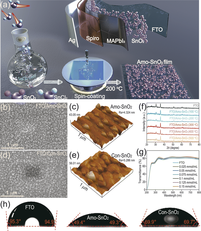 |
| | Fig. 1 (a) Schematic diagram of the proposed strategy for preparing Amo-SnO2 film. SEM images of (b) Amo-SnO2 and (d) Con-SnO2 film by calcination at 200 °C. AFM images of (c) Amo-SnO2 and (e) Con-SnO2 film. (f) XRD patterns of the Amo-SnO2 films at different calcination temperatures. (g) Optical Transmittance of Amo-SnO2 films prepared with different concentrations of precursor solution and followed by calcination at 200 °C. (h) Contact angle images of SnO2 films and FTO substrates. | |
Experimental section
Experimental materials and reagents
Acetonitrile (ACN, 99.9%) and chlorobenzene (CB, 99.5%) were purchased from Sigma-Aldrich. N,N-dimethylformamide (DMF, 99.9%), dimethyl sulfoxide (DMSO, 99.8%), tin oxide powders (99.9%), anhydrous tin chloride (99.99%) and SnCl2·2H2O were obtained from Aladdin. Methyl iodide (MAI, 99.5%) was purchased from Xi'an Yuri Solar Co., Ltd. Lead iodide (PbI2, 99.9%), lithium bis (trifluoromethanesulfonyl) imide (Li-TFSI, 99.95%), 4-tert-butylpyridine (TBP, 96.0%) and 2,2′, 7,7′-tetrakis(N,N-di-p-methoxyphenylamine)-9,9-spirobifluorene (Spiro-OMeTAD, 99.86%) were purchased from Advanced Election Technology Co., Ltd. Fluorine-doped tin oxide glasses (FTO, 14 Ω, 1.5 × 1.5 cm) were purchased from Advanced Election Technology Co., Ltd. Ultrapure water with 18 MΩ was obtained from device of Ultrapure Water System (Corning Technology Development Co., Ltd, PRO-3200, Chengdu). All chemicals were used as achieved without further purification process.
Preparation of SnO2 film
For amorphous SnO2 film, the FTO substrates were cleaned consecutively with detergent, acetone, isopropanol, ethanol, and deionized water for 50 minutes through ultrasonic cleaning, and then dried at 75 °C in an air oven for several hours before the ozone treatment for 10 minutes. Subsequently, the SnCl2 precursor was prepared by dissolving 22.5 mg of SnCl2·2H2O into 1 mL of DMF and stirring for 10 minutes at room temperature to form SnCl2/DMF solution with concentration of 0.1 mmol mL−1. Then, 35 μL of the SnCl2 precursor solution was spin-coated onto cleaned FTO substrate at 3000 rpm for 30 seconds and followed by annealing at various temperatures from 100 to 350 °C for 1 hour to generate amorphous SnO2 electron transport layer.
For crystal SnO2 film (Con-SnO2), 22.5 mg of SnCl2·2H2O was dissolved in 1 mL of ethanol to form the SnCl2/ethanol solution with concentration of 0.1 mmol mL−1. Then, the precursor solution was spin-coated onto clean FTO substrate with 3000 rpm for 30 s and followed by annealing at 180 °C for 1 h to obtain the Con-SnO2 film.20
Preparation of perovskite solar cell device
The prepared SnO2 electron transport layer was treated with ozone for 15 min prior to depositing perovskite precursor solution in order to remove organics on the surface of the SnO2 electron transport layer. After that, 35 μL of perovskite precursor solution (containing the MAI and PbI2 at 1![[thin space (1/6-em)]](https://www.rsc.org/images/entities/char_2009.gif) :1 of stoichiometric ratio in a mixed solvent with VDMF:VDMSO = 4:1 to keep the concentrations of both MAI and PbI2 at 1.25 mmol mL−1) was dropped onto SnO2 ETL film under conditions of 1000 rpm for 3 s and then 4000 rpm for 30 s and followed by dropping 200 μL of chlorobenzene at eighth second before annealing at 100 °C for 10 minutes. The hole transport layer (HTL) precursor solution was prepared by dissolving 17.5 μL of Li-TFSI acetonitrile (520 mg mL−1) solution, 28.8 μL of tBP and 72.3 mg of Spiro-OMeTAD solution in 1 mL of chlorobenzene into a 2 mL of flask and followed by stirring for 12 hours at nitrogen atmosphere. Then, 20 μL of HTL precursor was spin-coated onto perovskite layer at 5000 rpm for 30 s and then ripened in a drying oven at room temperature overnight in air. Finally, Ag electrode with a thickness of ∼100 nm was deposited onto the surface of the hole transport layer as the top electrode under vacuum condition with 4 × 10⁻³ Pa and a current of 40 A using a heating boat for 20 minutes.
:1 of stoichiometric ratio in a mixed solvent with VDMF:VDMSO = 4:1 to keep the concentrations of both MAI and PbI2 at 1.25 mmol mL−1) was dropped onto SnO2 ETL film under conditions of 1000 rpm for 3 s and then 4000 rpm for 30 s and followed by dropping 200 μL of chlorobenzene at eighth second before annealing at 100 °C for 10 minutes. The hole transport layer (HTL) precursor solution was prepared by dissolving 17.5 μL of Li-TFSI acetonitrile (520 mg mL−1) solution, 28.8 μL of tBP and 72.3 mg of Spiro-OMeTAD solution in 1 mL of chlorobenzene into a 2 mL of flask and followed by stirring for 12 hours at nitrogen atmosphere. Then, 20 μL of HTL precursor was spin-coated onto perovskite layer at 5000 rpm for 30 s and then ripened in a drying oven at room temperature overnight in air. Finally, Ag electrode with a thickness of ∼100 nm was deposited onto the surface of the hole transport layer as the top electrode under vacuum condition with 4 × 10⁻³ Pa and a current of 40 A using a heating boat for 20 minutes.
Characterization of solar cell device
The photo-electric properties of prepared PSCs were analyzed by a standard solar cell device (San-EI Electric, XEC-300M2, Japan) equipped with a light source of atmospheric mass (AM) 1.5 G with 100 mW cm−2 of incident light power density. The effective testing area of the device was kept at 0.057 cm2, and the test voltage was ranging from −0.2 to 1.2 V. Electrochemical workstation (ELS, CH Instruments, CHI 600D, China) was used for measuring the electrochemical AC impedance of PSCs, with 0.8 V of initial voltage, 1 × 10⁶ Hz of high frequency and 1 Hz of low frequency. Other testing parameters including the amplitude and settling time were used based on the default values of workstation. Solar cell testing system (Desai Optoelectronics, 7-SCSpec IPCE, China) was employed for external quantum efficiency (EQE) analysis of PSCs device, with testing wavelength ranging from 300 to 800 nm.
Materials characterizations
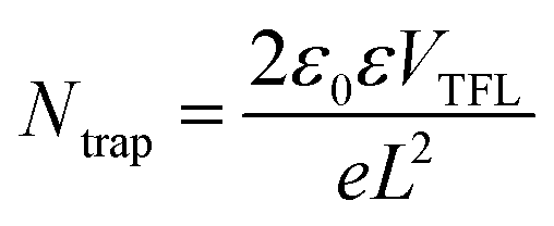
X-ray diffraction meter (XRD, Bruker D8, Germany) was employed to analyze the crystal structure of films with scanning speed at 10° min−1, step size at 0.026°, and scanning range from 20 to 80°. The absorption and transmission spectra of films were measured by an UV-Vis spectrophotometer (UV, Shimadzu, UV-1800, Japan) in a wavelength range of 500–1100 nm at room temperature. Fluorescence spectrophotometer (PL, Hitachi, F-7100, Japan) was used for testing the photoluminescence intensity of perovskite films with an excitation wavelength of 460 nm and emission wavelength from 650 to 850 nm. Scanning Electron Microscope (SEM, Hitachi, SU8020, Japan) was employed to observe the surface morphology of films. The electronic structure of prepared films was analyzed by X-ray photoelectron spectroscopy (XPS, Escalab, 250 Xi, America). Atomic Force Microscope (AFM, Shimadzu, SPM9700, Japan) was used for testing the surface roughness of films. Fourier Transform infrared spectroscopy (FTIR, Thermo Fisher, IS55, America) was used for analyzing the organic groups in films. The hydrophilicity of the films was measured by a video optical contact angle measuring instrument (CA, Dataphysics, OCA25, Germany). Valence band of films was calculated based on formula (1), where EVB is valence band, φ is the work function of the XPS instrument (φ = 4.55 eV), EVB, XPS is the valence band position versus XPS. Defect state density is determined from formula (2), where ε is the vacuum dielectric constant, ε0 is the relative dielectric constant, L is the thickness of the perovskite film, e is the elemental charge, VTFL is the trap filling limit voltage at the transition point of the ohmic and trap filling limit regions, Ntrap is the defect density of states.| | |
EVB = φ + EVB, XPS − 0.44
| (1) |
| |
 | (2) |
Results and discussion
The surface morphology of SnO2 film
The entire process from preparing precursor solution of SnCl2 to generating amorphous SnO2 film is described in Fig. 1a. It is noted that the stability of precursor solution plays a key role in obtaining the SnO2 film with high quality and reproducible properties among batch of experiments. The prepared SnCl2 precursor exhibits acceptable chemical stability with clear and transparent state up to six months in Fig. S1.† The SnO2 film is then produced by spin coating of precursor solution at different annealing temperatures. In Fig. S2,† with increasing the annealing temperature more than 200 °C, the surface of the film becomes rough and appears obvious cracks, which is not beneficial to electron transfer and the growth of perovskite layer, caused by high annealing temperature leads to more oxygen defects and pinholes in the films.28 Therefore, 200 °C is optimal to obtain SnO2 film with high quality (denoted as Amo-SnO2). The morphologies of Amo-SnO2 and Con-SnO2 films are then compared by scanning electron microscopy (SEM) and atomic force microscopy (AFM) in Fig. 1b–e and S3.† It can be seen that comparing with the Con-SnO2 film, the Amo-SnO2 film exhibits uniform and smooth surface covered onto FTO substrate, as demonstrated by the decreased surface roughness (Ra) of 4.324 nm for Amo-SnO2 than that of 5.286 nm for Con-SnO2 films. Then, XRD pattern demonstrates the amorphous structure of prepared SnO2 film in Fig. 1f. There are no detectable characteristic peaks corresponding to standard SnO2 with calcination temperature from 100 to 500 °C, indicating that the formation of amorphous structure of SnO2 is independent of its calcination temperature. Similar results are also obtained when SnO2 is covered onto glass substrate instead of FTO in Fig. S4.† Fig. S5† shows the XRD pattern of Con-SnO2 thin film, the peak of Con-SnO2 corresponds to the standard SnO2: JCPDS SnO2-PDF#41-1445. The formation of SnO2 using ethanol is similar with using water as solvents to provide hydroxy group to form Sn(OH)2. The function of DMF is possibly to form weak Sn–O–N bond instead of Sn–OH bond. The intermediate structure of Sn–O–N can inhibit the formation of crystal SnO2, resulting in the amorphous SnO2. For PSCs device, high optical transmittance of functional layers including HTL and ETL indicates less photons harvesting by functional layers and high photons utilization efficiency by active layers such as perovskite layer for improved performance of PSCs device. In Fig. 1g, the optical transmittance (300–800 nm) of Amo-SnO2 films is optimized by modulating concentrations of SnCl2 precursor. Up to 83.661% of optical transmittance is obtained with 0.1 mmol mL−1 of precursor solution. Identical result is also described by replacing FTO with glass substrates to obtain 88.782% of optical transmittance in Fig. S6.† The optimal optical transmittance of SnO2 film is also demonstrated up to 82.874% at 200 °C of calcination temperature in Fig. S7.† Over high temperature (>200 °C) brings some micro-cracks on the surface of film, resulting in decreased optical transmittance. It is noted that hydrophilic surface of SnO2 film can facilitate the adsorption and growth of perovskite film. Therefore, the surface hydrophilicity of SnO2 films is evaluated by contact angle analysis in Fig. 1h. Decreased contact angle with 49.4° for Amo-SnO2 than that with 69.9° for Con-SnO2 indicates the enhanced hydrophilicity of Amo-SnO2. Generally, surface roughness of film is positive correlated with its hydrophilic efficacy. However, for Amo-SnO2, hydrophilic residual including chloride ion and DMF exist on the surface of film as demonstrated from Fig. 2c and S8,† resulting in the increased hydrophilic efficacy than that of Con-SnO2. In addition, the growth process of Amo-SnO2 film is analyzed by infrared spectroscopy tests in Fig. S8.† From the magnified FTIR spectra, trace of C–H and C![[double bond, length as m-dash]](https://www.rsc.org/images/entities/char_e001.gif) O groups can be detected in Amo-SnO2-calcination, indicating the residual DMF on the surface of Amo-SnO2 film. This result also demonstrates the in situ growth of Amo-SnO2 film by converting SnCl2-DMF into amorphous SnO2 film.
O groups can be detected in Amo-SnO2-calcination, indicating the residual DMF on the surface of Amo-SnO2 film. This result also demonstrates the in situ growth of Amo-SnO2 film by converting SnCl2-DMF into amorphous SnO2 film.
Characterizations of electronic structure
X-ray photoelectron spectroscopy (XPS) is used to analyze the surface electronic structure of Amo-SnO2 and Con-SnO2 films. In Fig. S9,† detectable elements including Sn and O in both two kinds of films indicate the successful preparation of SnO2 films without impurities. In Fig. 2a, it is found that there are peaks at 486.83 and 495.23 eV (corresponding to Sn 3d5/2) for Amo-SnO2 and SnO2 powder, respectively, indicating the existence of Sn4+ on the surface of Amo-SnO2 film. Absence of Sn2+ is also demonstrated by the disappearance of peak at 486.0 eV for Amo-SnO2. For SnO2 film, the O 1s XPS (Fig. 2b) peaks at ∼530.4 eV and ∼531.8 eV can be attributed to Sn–O bond and hydroxyl (–OH) adsorbed on the surface of film, respectively.21,22,29,30 The peak area ratio of Sn–O to hydroxyl for Amo-SnO2 and Con-SnO2 are calculated as 0.95 and 0.87, respectively, indicating the increased absorption of hydroxyl for Amo-SnO2 than that for Con-SnO2. Owing to the increased hydrophilic capability of Amo-SnO2 over Con-SnO2 (Fig. 1h), Amo-SnO2 tends to absorb water molecule from air before XPS analysis. Increased hydrophilic surface of Amo-SnO2 film exhibits advantage in depositing perovskite film toward high-performance PSCs. Compared with SnO2 powder, the characteristic peaks of Sn 3d and O 1s of Amo-SnO2 films exhibit minor shifts to high binding energy, which is caused by the residual chloride ions on its surface to passivate the vacancy of oxygen.25,31 Besides, there exists Cl 2p peak for the Amo-SnO2 (Fig. S9† and 2c), indicating the less amount of chloride ions on its surface. Comparing with SnCl2 powder, the binding energy of Cl− moves towards higher energy for Amo-SnO2 film in Fig. 2c, which can be attributed to the formation of Sn–Cl bond, resulting in some oxygen vacancies existing on the surface.31 Therefore, replacing the ethanol with DMF solvent can introduce less amounts of chloride ions on the surface of amorphous SnO2 film. The presence of Cl− contributes to growing perovskite films, passivating the defects at the interface of Amo-SnO2 and perovskite, and inhibiting the non-radiative recombination of carriers.32,33 It is noted that negligible difference for Sn 3d and O 1s spectra is found between Con-SnO2 and SnO2 powder, demonstrating that there is almost no Cl− in Con-SnO2 (Fig. 2a and b). Then, semiconductive properties of SnO2 films are analyzed in Fig. 2d. Valence band is calculated based on formula (1) described in experimental sections. Similar valence bands are obtained for the Amo-SnO2 (7.43 eV) and SnO2 powder (7.23 eV). In contrast, higher band gap up to 3.63 eV is observed for Amo-SnO2 than that for SnO2 powder with 3.58 eV (Fig. 2e), possibly caused by the special amorphous structure of SnO2. Besides, ultraviolet photoelectron spectroscopy (UPS) is performed to analyze the conduction bands of films in Fig. S10.† Combined with the band gap in Fig. 2e, the conduction band of the Amo-SnO2 and Con-SnO2 are determined as 3.8 and 3.79 eV. Finally, the energy levels of the Amo-SnO2, SnO2 powder, Con-SnO2 and the perovskite active layer are described in Fig. 2f. This diagram indicates the appropriate conduction match between Amo-SnO2 and perovskite active layer, promoting the extraction and transport of photo-generated electrons by active layer.
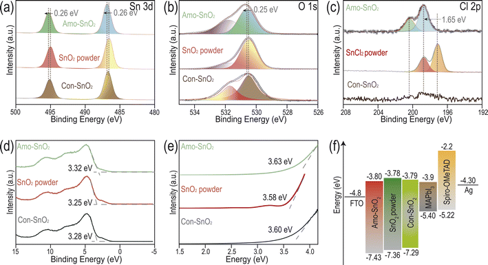 |
| | Fig. 2 High-resolution XPS spectra of SnO2 based films: (a) Sn 3d, (b) O 1s, (c) Cl 2p. (d) Valence band spectra of films. (e) Bandgap diagram of films. (f) Energy level diagram of each layer in PSCs. | |
Characterizations of perovskite solar cell device
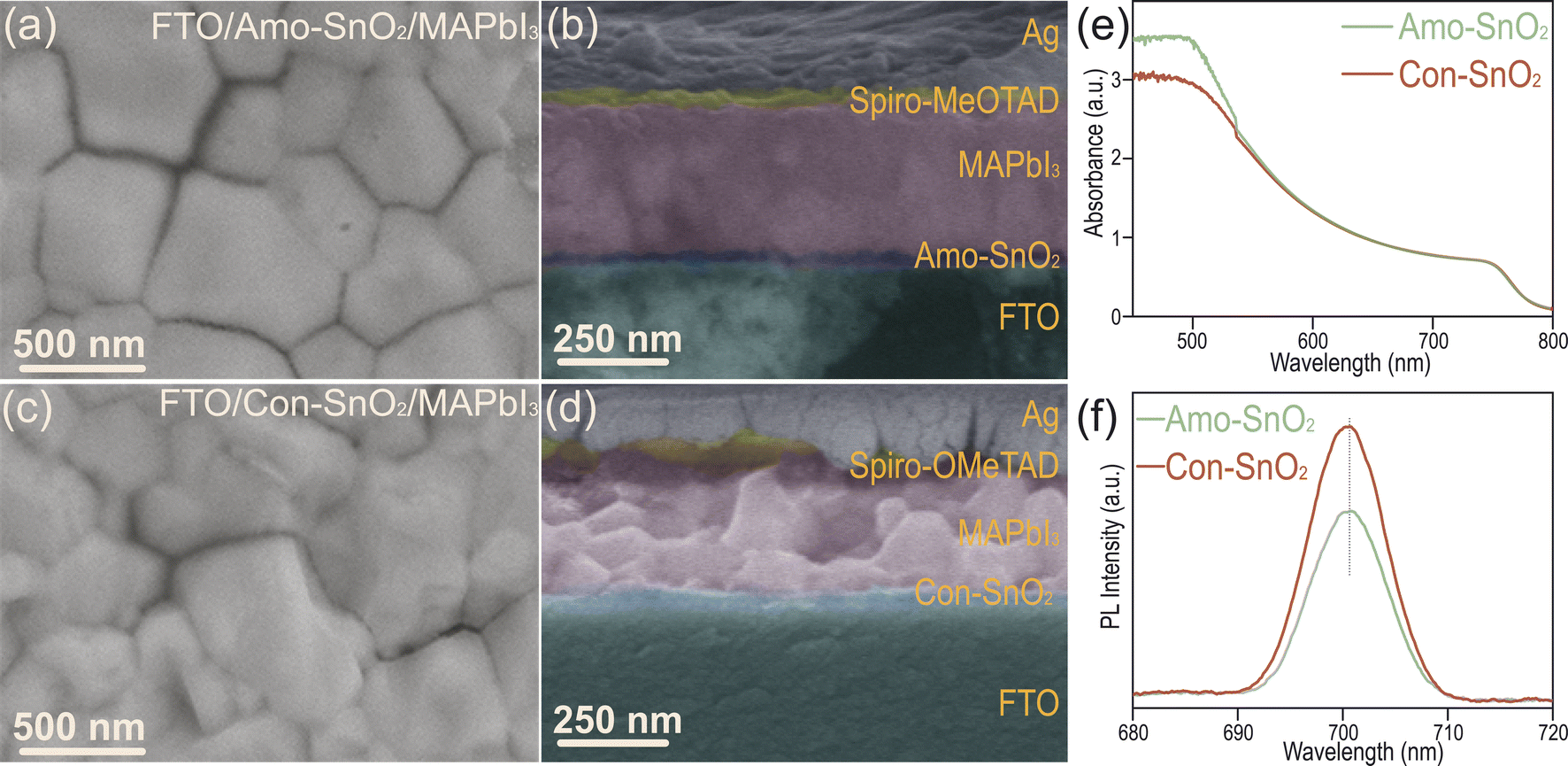
The morphologies of perovskite solar cell devices are characterized by SEM in Fig. 3a–d. Smooth and dense surface with larger grain size is observed for perovskite layer coated onto Amo-SnO2 than that coating onto Con-SnO2, which can promote the transfer of photo-generated electrons and reduce recombination of non-radiative charges. Cross-sections of PSCs are then explored in Fig. 3b and d. Dense contact between ETL and perovskite layers is obtained for Amo-SnO2 and the thickness of each layer of the PSCs are determined as ∼23 nm for Amo-SnO2 (ETL), ∼290 nm for MAPbI3 (active layer), ∼100 nm for Sprio-OMeTAD (HTL), and ∼100 nm for Ag electrode, respectively. Besides, crystal structure of perovskite layers coated separately onto Amo-SnO2 and Con-SnO2 films are analyzed in Fig. S11.† The intensity of diffraction peak at 14.65° (corresponding to (110) plane) for Amo-SnO2 is 1.45 times higher than that for Con-SnO2 (Fig. S11†). Moreover, for Amo-SnO2 films prepared at different annealing temperatures, 200 °C of annealing temperature results in higher crystallinity of MAPbI3 in Fig. S12,† which is possibly caused by over high annealing temperature can deteriorate the surface structure of SnO2. In Fig. 3e and f, increased optical absorption (380–760 nm) and decreased fluorescence emission intensity at 700 nm for perovskite layer coated onto Amo-SnO2 layer are obtained than that onto Con-SnO2 layer. Above results indicate that comparing with Con-SnO2 layer, the Amo-SnO2 layer is more suitable for growing perovskite with dense contact and high quality to provide higher electron extraction and transport efficacy with less non-radiation loss for high-performance device.
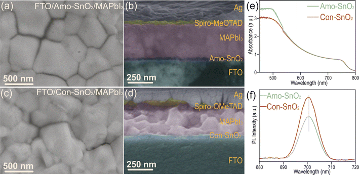 |
| | Fig. 3 SEM images of MAPbI3 film coated onto (a)Amo-SnO2 and (c) Con-SnO2 films. Cross sections of PSCs using (b) Amo-SnO2 and (d) Con-SnO2 as ETL. (e) Ultraviolet visible absorbance and (f) PL spectra of perovskite films deposited separately onto Con-SnO2 and Amo-SnO2 layers. | |
Performance of perovskite solar cell device
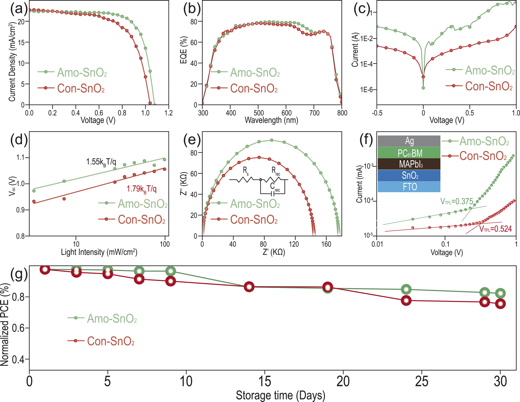
In order to further study the function of Amo-SnO2 as an electron transport layer in perovskite solar cells, the n-i-p type of PSCs with structure of FTO/Amo-SnO2/MAPbI3/Spiro-MeOTAD/Ag are prepared. For Amo-SnO2, the performance of PSCs is optimized by modulating the concentrations of precursor solutions of SnCl2 and calcination temperature in Fig. S13 and S14.† The optimal parameters are kept at 0.1 mmol mL−1 of concentration and 200 °C of calcination temperature. Champion device with corresponding parameters including open circuit voltage (Voc), short-circuit current density (Jsc), fill factor (FF) and photovoltaic conversion efficiency (PCE) are summarized in Tables S1 and S2.† In Fig. 4a, the photoelectric conversion efficiency (PCE) of using Amo-SnO2 as ETL reaches up to 17.64%, which is significantly higher than that of using Con-SnO2 as ETL PSCs (16.43% of PCE). This result is further demonstrated using batch of PSCs with twenty samples for PCE analysis by reverse scan in Fig. S15.† Average PCE for Amo-SnO2 and Con-SnO2 are 16.59 ± 0.59 and 15.34 ± 0.74, respectively. Forward and reverse scan of J–V curves are provided in Fig. S16.† For Amo-SnO2, 15.44% and 17.38% of PCE are obtained for forward and reverse scan, respectively, comparing with the 13.87% and 16.19% for Con-SnO2. Therefore, less hysteresis effect is obtained by Amo-SnO2 than by Con-SnO2 used as ETL in PSCs. To exploring the recombination of charge carriers occurring on the surface and inside of perovskite thin films, the external quantum efficiency (EQE) analysis is performed using the champion device. In Fig. 4b, the device of using Amo-SnO2 as ETL owns higher optical response than that using Con-SnO2 as ETL, resulting in increased Jsc of device using Amo-SnO2 as ETL. The surface and internal defects of devices are evaluated by dark current density analysis. In Fig. 4c, dark current curve of device using Amo-SnO2 as ETL indicates the decreased leakage current at the low-voltage scale, which suggests the dense interfacial contact between Amo-SnO2 ETL and the active layer. Furthermore, photo-generated carrier recombination efficiency of device using various ETL can be illustrated by the light intensity and open circuit voltage curve in Fig. 4d. For PSCs with structure of FTO/SnO2/MAPbI3/Spiro-MeOTAD/Ag, Amo-SnO2 exhibits smaller ideal factor (1.55) than Con-SnO2 (1.79), indicating the suppression of non-radiative recombination, reduction and inhibition of Voc losses and leakage current of PSCs using Amo-SnO2 as ETL. Besides, the recombination of charge carriers in devices are analyzed using electrochemical impedance spectroscopy (EIS) in Fig. 4e. In the Nyquist plots, both devices using Amo-SnO2 and Con-SnO2 as ETL exhibit obvious semi-circular curves. Comparing with Con-SnO2, device using Amo-SnO2 as ETL obtains a larger semi-circular diameter, indicating higher composite resistance, larger composite resistance and lower probability of carrier recombination, which is beneficial for PSCs. To verify the carrier recombination of the device under light conditions, EIS map under light conditions are conducted in Fig. S17.† The composite resistance (Rrec = 52.48 kΩ) of Amo-SnO2 is significantly higher than that of Con-SnO2 (Rrec = 41.09 kΩ). In PSCs, higher Rrec and smaller Rs indicate lower carrier recombination and higher efficiency of extracting electrons, which is conducive to the performance of the PSCs. Combined EIS results under both light and dark conditions demonstrate weak carrier recombination efficiency when Amo-SnO2 film is employed as ETL. In addition, the space charge limited current method (SCLC) is used to quantitatively characterize the defect state density of the PSCs. Defect densities of electrons are analyzed using the device without hole transport layer (FTO/SnO2/MAPbI3/PC61BM/Ag). In Fig. 4f, the VTFL of the champion device using Con-SnO2 and Amo-SnO2 as electron transport layers are 0.524 V and 0.375 V, respectively. The corresponding electrons trap densities (Ntrap) using Amo-SnO2 as ETL is obtained with 4.839 × 1015 cm−3, which is significantly lower than that using Con-SnO2 as ETL (6.762 × 1015 cm−3). Finally, the long-term stability of the device is evaluated in Fig. 4g. After 30 days of storage, the device using Amo-SnO2 as ETL still maintains 83.33% of the initial PCE in the glove box, in contrast with only 76.09% for Con-SnO2, indicating the excellent stability of device using Amo-SnO2 as ETL. Moreover, the prepared SnCl2/DMF precursor also demonstrates long-time of stability over conventional SnCl2/EtOH solution. In Fig. S18,† only 0.63% of PCE is reduced for Amo-SnO2 after nine months of storage of SnCl2/DMF solution at room temperature, in contrast with 1.85% of PCE reduction for Con-SnO2 with identical treating process. Long time stability of PSCs using Amo-SnO2 as ETL can be attributed to the special amorphous structure of SnO2 favoring to maintain the long-time structure stability and keep dense contact between Amo-SnO2 ETL and the active layer.
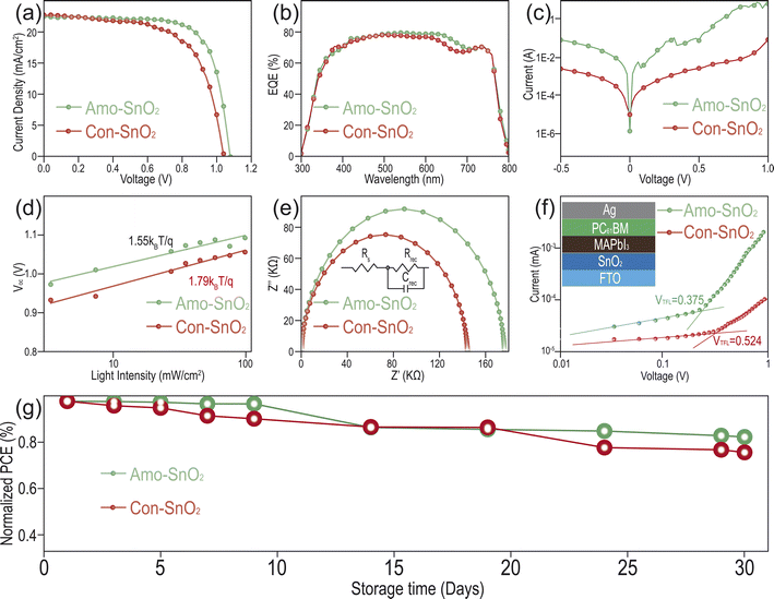 |
| | Fig. 4 (a) J–V, (b) EQE, (c) dark current density, (d) voltage changing with light intensity, (e) EIS in dark conditions at 0.8 V bias, (f) SCLC and (g) working stability curves of the devices using different electron transport layers. | |
Conclusions
In summary, a facile in situ one step method is proposed for preparing amorphous SnO2 film as the ETL. The as-synthesized Amo-SnO2 film owns superior electrical conductivity, optimized band gap, and lower trap density compared with Con-SnO2. The proposed method simplifies the preparation process of ETL in n-i-p type of device and extends the application of amorphous materials in PSCs. The device based on the Amo-SnO2 thin film attains champion PCE up to 17.64% and 1.09 V of Voc. In addition, the device using Amo-SnO2 as ETL presents excellent stability up to 30 days with only 83.33% of reduction of initial PCE. Finally, this work provides a viable method for the application of amorphous electron transport layers in perovskite solar cells.
Author contributions
The manuscript was written through contributions of all authors. All authors have given approval to the final version of the manuscript.
Conflicts of interest
The authors declare no conflict of interest.
Acknowledgements
This work is supported by Major Cultivation Project of Gansu Province University Research and Innovation Platform (2024CXPT-03); The financial support of this work was provided by Gansu Provincial Natural Science Foundation of China (6B0023); Science Foundation of Lanzhou Jiaotong University (1200061037); Gansu Provincial Department of Education: Major Cultivation Project for College and University Scientific Research Innovation Platforms (2024GJPT-01).
Notes and references
- A. Kojima, K. Teshima, Y. Shirai and T. Miyasaka, J. Am. Chem. Soc., 2009, 131, 6050–6051 CrossRef CAS PubMed.
- H. P. Zhou, Q. Chen, G. Li, S. Luo, T. B. Song, H. S. Duan, Z. Hong, J. B. You, Y. S. Liu and Y. Yang, Science, 2014, 345, 542 CrossRef CAS PubMed.
- J. Song, W. N. Zhang, D. Wang, K. M. Deng, J. H. Wu and L. Zhang, Sol. Energy, 2019, 185, 508–515 CrossRef CAS.
- M. M. Hu, L. Z. Zhang, S. Y. She, J. C. Wu, X. Y. Zhao, X. G. Li, D. Wang, J. Miao, G. J. Mi, H. Chen, Y. Q. Tian, B. M. Xu and C. Cheng, Sol. RRL, 2020, 4, 1900331 CrossRef CAS.
- Q. Jiang, Z. M. Chu, P. Y. Wang, X. L. Yang, H. Liu, Y. Wang, Z. G. Yin, J. L. Wu, X. W. Zhang and J. B. You, Adv. Mater., 2017, 1703852 CrossRef PubMed.
- C. Luo, G. H. J. Zheng, F. Gao, X. J. Wang, C. L. Zhan, X. Y. Gao and Q. Zhao, Nat. Photonics, 2023, 17, 856–864 CrossRef CAS.
- Q. Jiang, L. Q. Zhang, H. L. Wang, X. L. Yang, J. H. Meng, H. Liu, Z. G. Yin, J. L. Wu, X. W. Zhang and J. B. You, Nat. Energy, 2017, 2, 16177 CrossRef CAS.
- N. J. Jeon, J. H. Noh, W. S. Yang, Y. C. Kim, S. C. Ryu, J. W. Seo and S. I. Seok, Nature, 2015, 517, 476–480 CrossRef CAS PubMed.
- W. S. Yang, J. H. Noh, N. J. Jeon, Y. C. Kim, S. C. Ryu, J. W. Seo and S. I. Seok, Science, 2015, 348, 1234–1237 CrossRef CAS PubMed.
- N. X. Li, S. X. Tao, Y. H. Chen, X. X. Niu, C. K. Onwudinanti, C. Hu, Z. W. Qiu, Z. Q. Xu, G. H. J. Zheng, L. G. Wang, Y. Zhang, L. Li, H. F. Liu, Y. Z. Lun, J. W. Hong, X. Y. Wang, Y. Q. Liu, H. P. Xie, Y. L. Gao, Y. Bai, S. H. Yang, G. Brocks, Q. Chen and H. P. Zhou, Nat. Energy, 2019, 4, 408–415 CrossRef CAS.
- M. H. Li, J. J. Zhou, L. G. Tan, H. Li, Y. Liu, C. F. Jiang, Y. R. Ye, L. M. Ding, W. Tress and C. Y. Yi, Int. J. Innov., 2022, 3, 100310 CAS.
- H. Min, D. Y. Lee, J. Kim, G. Kim, K. S. Lee, J. Kim, M. J. Paik, Y. K. Kim, K. S. Kim, M. G. Kim, T. J. Shin and S. I. Seok, Nature, 2021, 598, 444–450 CrossRef CAS PubMed.
- Y. C. Chen, Q. Meng, L. R. Zhang, C. B. Han, H. L. Gao, Y. Z. Zhang and H. Yan, J. Energy Chem., 2019, 35, 144–167 CrossRef.
- L. Y. Lin, T. W. Jones, T. C. J. Yang, N. W. Duffy, J. H. Li, L. Zhao, B. Chi, X. B. Wang and G. J. Wilson, Adv. Funct. Mater., 2020, 31, 2008300 CrossRef.
- K. Valadil, S. Gharibi, R. T. Ledari, S. Akin, A. Maleki and A. E. Shalan, Environ. Chem. Lett., 2021, 19, 2185–2207 CrossRef.
- L. J. Zuo, H. X. Guo, D. W. deQuilettes, S. Jariwala, N. D. Marco, S. Q. Dong, R. DeBlock, D. S. Ginger, B. Dunn, M. K. Wang and Y. Yang, Sci. Adv., 2017, 3, e1700106 CrossRef PubMed.
- J. S. Xie, K. Huang, X. G. Yu, Z. R. Yang, K. Xiao, Y. P. Qiang, X. D. Zhu, L. B. Xu, P. Wang, C. Cui and D. Yang, ACS Nano, 2017, 11, 9176–9182 CrossRef CAS PubMed.
- Z. P. Wang, Q. Q. Lin, F. P. Chmiel, N. Sakai, L. M. Herz and H. J. Snaith, Nat. Energy, 2017, 2, 17135 CrossRef CAS.
- W. J. Ke, D. W. Zhao, A. J. Cimaroli, C. R. Grice, P. L. Qin, Q. Liu, L. B. Xiong, Y. F. Yan and G. J. Fang, J. Mater. Chem. A, 2015, 3, 24163–24168 RSC.
- W. J. Ke, G. J. Fang, Q. Liu, L. B. Xiong, P. L. Qin, H. Tao, J. Wang, H. W. Lei, B. R. Li, J. W. Wan, G. Yang and Y. F. Yan, J. Am. Chem. Soc., 2015, 137, 6730–6733 CrossRef CAS PubMed.
- J. J. Zhang, H. Y. Wang, Q. Y. Yang, C. Gao, C. X. Gao and X. Z. Liu, Opt. Mater., 2023, 137, 113518 CrossRef CAS.
- M. Shi, T. C. Bai, S. S. Du, H. M. Sha, H. Chen, X. H. Ma, Y. D. Xu and Y. Q. Chen, Acta, 2023, 444, 141985 CAS.
- Z. L. Zhu, Y. Bai, X. Liu, C. C. Chueh, S. H. Yang and A. K. Y. Jen, Adv. Mater., 2016, 28, 6478–6484 CrossRef CAS PubMed.
- G. Yang, C. Chen, F. Yao, Z. L. Chen, Q. Zhang, X. L. Zheng, J. J. Ma, H. W. Lei, P. L. Qin, L. B. Xiong, W. J. Ke, G. Li, Y. F. Yan and G. J. Fang, Adv. Mater., 2018, 30, 1706023 CrossRef PubMed.
- H. R. Tian, J. J. He, X. Y. Liu, Q. Li, D. Liu, B. B. Shen, S. Yang, Q. Niu and Y. Hou, Small Sci., 2023, 3, 2200112 CrossRef CAS.
- C. Zhang, X. T. Yin, Y. X. Guo, H. X. Xie, D. Liu and W. X. Que, Phys. Chem. Chem. Phys., 2022, 24, 18896 RSC.
- H. B. Lee, N. Kumar, M. M. Ovhal, Y. J. Kim, Y. M. Song and J. W. Kang, Dopant-Free, Adv. Funct. Mater., 2020, 30, 2001559 CrossRef CAS.
- W. Ke, D. Zhao, A. J. Cimaroli, C. R. Grice, P. Qin, Q. Liu, L. Xiong, Y. Yan and G. Fang, Effects of annealing temperature of tin oxide electron selective layers on the performance of perovskite solar cells, J. Mater. Chem. A, 2015, 3, 24163 RSC.
- S. W. Shi, J. L, T. l. Bu, S. L. Yang, J. Y. Xiao, Y. Peng, W. Li, J. Zhong, Z. L. Ku, Y. B. Cheng and F. Z. Huang, RSC Adv., 2019, 9, 9946–9950 RSC.
- J. Li, T. L. Bu, Y. F. Liu, J. Zhou, J. L Shi, Z. L. Ku, Y. Peng, J. Zhong, Y. B. Cheng and F. Z. Huang, ChemSusChem, 2017, 11, 2898–2903 CrossRef PubMed.
- J. W. Liang, Z. L. Chen, G. Yang, H. B. Wang, F. H. Ye, C. Tao and G. J. Fang, ACS Appl. Mater. Interfaces, 2019, 11, 23152–23159 CrossRef CAS PubMed.
- P. Y. Wang, B. B. Chen, R. J. Li, S. L. Wang, N. Y. Ren, Y. C. Li, S. Mazumdar, B. Shi, Y. Zhao and X. D. Zhang, ACS Energy Lett., 2021, 6, 2121–2128 CrossRef CAS.
- J. B. Wu, C. Zhen and G. Liu, Rare Met., 2022, 41, 361–367 CrossRef CAS.
|
| This journal is © The Royal Society of Chemistry 2024 |

 Open Access Article
 This Open Access Article is licensed under a Creative Commons Attribution-Non Commercial 3.0 Unported Licence
 * and
Chenglong Wang*
* and
Chenglong Wang*